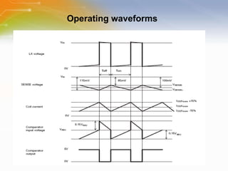
![Output current Adjustment by DC Control Voltage I OUTnom = 0.1/R S [for R S >0.27], where ADJ pin is floating I OUTdc = 0.08*V ADJ /R S [for 0.3< V ADJ <2.5V]](https://image.slidesharecdn.com/zetexzxld1350-110316020222-phpapp01/85/ZXLD1350-High-Power-LED-Driver-9-320.jpg)
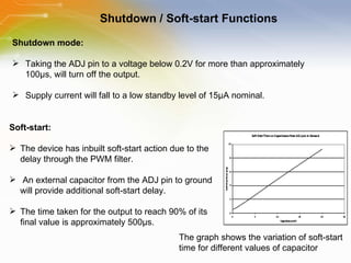
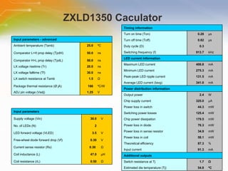


The document provides an overview of the ZXLD1350 LED driver chip, including its key features, internal block diagram, typical applications, and basic operating principles such as PWM dimming and output current adjustment. The chip has an internal switch, 350mA current output, single pin control of on/off and brightness, and efficiencies up to 95%. It is suitable for applications such as low voltage lighting.