Ge8808 led datasheet

The GE8808B is a 3-channel constant current LED drive with resumable data transfers and internal display patterns. There are three open-drain constant current outputs, with a build-in PWM of grayscale. The range of input power is from +9V to +15V, and voltage-endurance of LED port is +12V. There is a built-in 12bits GAMMA correction module. PWM maximum refresh frequency is 8Khz, the GE8808B use the e-RZ (extended return to zero code)as the signal transmission mode, which can control the output current channel by channel and cascade infinitely,it provides two-signal data input as redundant control, which ensures the transmission of the signal if any single chip damages.In the displays the built-in display patterns that is suitable for those applications without a controller. There is the built-in power-on and power-off protection in the drive,which can enhance the service life of the chip. It alsohas the automatic test function while power on, working environment is from -40 ° C to + 85 ° C.

Recommended
More Related Content
What's hot
What's hot (20)
Similar to Ge8808 led datasheet
Similar to Ge8808 led datasheet (20)
Recently uploaded
Recently uploaded (20)
Ge8808 led datasheet
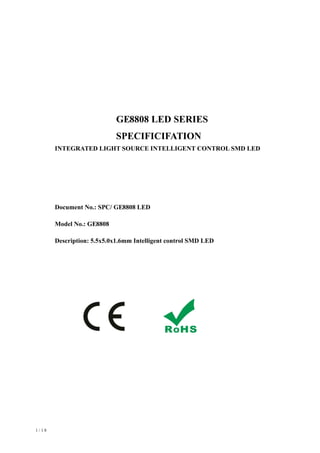
- 1. GE GE GE 80 80 8088 LED SERIES SPECIFICIFATION INTEGRATED LIGHT SOURCE INTELLIGENT CONTROL SMD LED Document No.: SPC/ 88 LED Model No.: 88 Description: 5.5x5.0x1.6mm Intelligent control SMD LED 1 / 1 8
- 2. kHz. The GE8808 l and cascade infinitely. GE8808 the customer to test. The GE8808 absence of signal input, GE8808 3. . Applications 2. . Features1 . General Descriptions GE8808The is a 3-channel constant current LED drive with resumable data transfers and internal display patterns. There are three open-drain constant current outputs, with a build-in PWM of grayscale. The range of input power is from +9V to +15V, and voltage-endurance of LED port is +12V. There is a built-in 12bits GAMMA correction module. PWM maximum refresh frequency is 8 use the e-RZ (extended return to zero code) as the signal transmission mode, which can control the output current channel by channe provides two-signal data input as redundant control, which ensures the transmission of the signal if any single chip damages. In the displays the built-in display patterns that is suitable for those applications without a controller. There is the built-in power-on and power-off protection in the drive, which can enhance the service life of the chip. It also has the automatic test function while power on, which is convenient for provides SOP8 packaging, working environment is from -40 °C to + 85 °C. ·LED Display ·LED lighting/light engineering ·12v operating supply voltage with 7805 module inside ·Default 17.5mA constant current output, the minimum is 11mA ·Use e-RZ code, serial data frequency 800kHz ·8bits data transfer, 12bits build-in GAMMA correction of PWM display ·Built-in PWM technology, supports 8kHz PWM refresh rate ·With resumable data transfer function, single chip damage does not infect data transmission ·Built-in display pattern for the applications without a controller ·Built-in automatic test mode, power-on and power-off protection ·ESD:2kV ·working environment is from -40 °C to + 85 °C ·Packaging:SOP8 2 / 1 8
- 3. GE GE GE GE 4 4 4 480 5 . Mechanical Dimensions: 88 mean white surface ,12-1 ma/channel ,capacitor integrated in 5050 (standard version) B mean white surface,12-1 ma/channel, without capacitor intergrated in 5050 -B mean black surface ,12-1 ma/channel ,capacitor integrated in 5050 -B mean black surface,12-1 ma/channel, without capacitor intergrated in 5050 Notes: 1. All dimensions are in millimeters. 2. Tolerance is ±0.1mm unless otherwise noted 4 . Product N aming 8088 8088 B8088 3 / 1 8 Mechanical Dimensions:mm 5.0 1.0 1.0 PCB Solder Pad LED Solder Pac 3.2 5.4 1.8 1.8 Top View Back View Solder Pad 1.VDH 6.SDI2 2.NA 5.SDI 3.SDO 4.GND
- 4. 8. . Pin Description 7. . Pin Configuration 6 . Block Diagram Pin Configuration with LED Pin name type Function VDH P 12V Power Supply GND P Chip Ground OUT1……OUT3 OUT Constant-current outputs,connected to LED SDI IN Series data input SDI2 IN Redundant series data input SDO OUT Series data output SDO 2 3 5 4 SDI2 GND 1 6VDH NA SDI SDO OUT3 2 3 4 7 6 5 VDH GND SDI 1 8OUT1 OUT2 SDI2 VDH GND LDO Output Driver Output Driver 12bits PWM generator 12bits PWM generator OUT2 Output Driver 12bits PWM generator OUT3OUT1 SDI 8bits Data 12bits Data OSC current Controller PORtest Digital Processor SDO SDI2 8bits->12bits GAMMA correction GE8808 GE8808 4 / 1 8
- 5. 1 0 . Maximum Ratings 9 . Equivalent Circuits of Input and Output 1 SDI/SDI2 2 SDO 3 OUT1、OUT2、OUT3 Characteristic Symbol Maximum Working Range Unit. Power Source VDH -0.4~15V V On-chip Power Source VCC -0.4~6V V Input Logic Voltage SDI -0.5~VDH+0.5 V Maximum output current IOUT 18 mA Output voltage-endurance VDS 15 V Ground current IGND 55 mA Power dissipation Pd 400 mW Working temperature TOP -40~85 o C Storage temperature Tstg -55~150 o C ESD HBM 2000 V (1)Stresses above there ratings may cause permanent damage. Exposure to absolute maximum condition for extended periods may degrade device reliability. These are stress ratings only and functional operation of the device at these or any other condition beyond those specified is not supported. (2)All voltage values are with respect to ground terminal. 5 / 1 8
- 6. 1 2 . Switching 1 1 . Electrical Characteristics Characteristic Symbol Symbol Measuring condition Min Typical Max Power supply VDH 9 12 15 V internal Power supply VCC 4 5 6 V High Input Logic Voltage VIH 4 V Low Input Logic Voltage VIL 1 V Output current IOUT VDH=12V 11 15 mA Static current Ichip 2.5 mA Power dissipation Pd 150 mW Current variation(channel) dIOUT Iout = 15mA, Vout = 1.2V ±1.5% ±3% % Current variation(chip) dIOUT2 ±3% ±6% % Current offset VS Power Source NA Voltage range of outputs VOUT 1.2 12 V External Power Res Rvdh VDH=12V 50 ohm External Power Cap Cvdh 0.1 uF Characteristics Characteristic Symbol Measuring condition Min Typical Max Unit. Internal Oscillator Frequency OSC 25 MHz PWM refresh rate 8 kHz Data refresh rate 30 1017 Hz Data refresh delay time 1024 points 700 us Internal program data refresh rate 100 Hz Channel output delay time 80 ns Current output rising time 18mA, VOUT=1V 40 ns Current output falling time 40 ns PWM pulse duration 240 ns RZ data frequency 400k 800k 1M Hz 6 / 1 8
- 7. 1 3 . Typical Application 7 / 1 8 OUT3 OUT3 OUT3OUT2 OUT2 OUT2OUT1 OUT1 OUT1 VDH VDH VDH SDO SDO SDO GND GND GND SD 1 SD 1 SD 1 SD 2 SD 2 S controller GND VDH GE8808 GE8808 GE8808
- 8. 1 4 . Data Format adopts the extended return to zero code (e-RZ) data transmission mode, 8bits data for single channel, each IC supports 3 channel for display. The transmission data is filtered internally to support the data anti-jitter function. The extension type is compatible with the traditional RZ code. So it is suitable for most of the RZ code controller in the market. Single code with 1:3 duty cycle and a standard 800kHz transmission speed. The maximum frequency can reach 1MHz. re-code the data before transmission. Data delay is less than 0.7us from chip to chip, meets the dynamic image needs. 0 code 1 code 3/4T1/4T 3/4T 1/4T T=1/800kHz <10us Intervals between code >300usReset Displaydata Ch01b7 Ch01b6 Ch01b5 Ch01b2 Ch01b1 Ch01b0 Ch00b7 Ch00b6 Ch00b5 Ch00b2 Ch00b1 Ch00b0 Ch02b7 Ch02b6 Ch02b5 Ch02b2 Ch02b1 Ch02b0 Ch(N+2)b7 Ch(N+2)b6 Ch(N+2)b5 Ch(N+2)b2 Ch(N+2)b1 Ch(N+2)b0 Ch(N+1)b7 Ch(N+1)b6 Ch(N+1)b5 Ch(N+1)b2 Ch(N+1)b1 Ch(N+1)b0 Ch(N+0)b7 Ch(N+0)b6 Ch(N+0)b5 Ch(N+0)b2 Ch(N+0)b1 Ch(N+0)b0 Reset Reset GE8808 GE8808 8 / 1 8
- 9. 1 6 . Data channel status testing during production Dual channel redundant control can be used to effectively avoid the failure of any single device damage, and reduce the damage rate of the driving system to one millionth. The SDI signal is used as the default transmission channel while the system is power on. The transmission channel priority is switched between SDI and SDI2 when the transmission data is abnormal. The device will choose the clear transmission channel after data detection. When the external control data is transmitted, SDI uses the 1-24bits received data as the display data, meanwhile, SDI2 will discard the 1-24bits data and use 25-48bits data as the display data. In the production process, any one of the abnormal data channel will not affect display because the chip uses dual SDI input. It is difficult to detect the problem data channel during the production process, which may cause the dual channel is equivalent to a single channel. In order to avoid this situation, the status of the data channel can be detected by using the test controller in the external control situation. While any channel appears Weld, short, open or other abnormal communication, the chip will display in white to facilitate the detection of problem position. Ch24b(N+1) Ch24bN Ch24b(N-1) Ch24b2 Ch24b1 Ch24b0 Ch24bN Ch24b(N-1) Ch24b2 Ch24b1 Ch24b0 Ch24b(N-1) Ch24b2 Ch24b1 Ch24b0 SDI SDI2 SDO 1 5 . Dual channel redundant control 9 / 1 8
- 10. principle of the series structure LED controller It is RGB LED series structure. Power supply voltage is 12V, and the LED constant current is 18mA. Different to the parallel architecture of 5V power supply and 54mA drive current, the series architecture can provide a better drive ability. The new architecture’s total drive current is only 1/3 of the original one, and Vds=4V. The power loading ability is better. In the series structure mode, when the internal MOS paralleling with the LED is open, the current flow into the LED and the LED lights. When the internal MOS paralleling with the LED is short, the current flow into the MOS device and the LED close. Switching the MOS device by PWM signal can lights on or off the LED. Because the LED adopts the RGB series mode, the chip LED output must be connected in the order of the diagram. The wrong connection way will cause the LED to not work properly. delay In order to prevent the large power interference from the LED switching, reduce the power circuit voltage fluctuations, has a built-in output hysteresis function. OUT1, OUT2, OUT3 will work in accordance with the 80ns interval sequence, to improve the system's anti-jamming performance. Meanwhile, the current peak output stagger will reduce the system EMI radiation, to meet environmental requirements. OUT1 T 2T T=80ns OUT2 OUT3 PWM1 PWM2 PWM3 OUT1 OUT2 OUT3 8808GE 1 7 . Working 1 8 . Stagger output 1 0 / 1 8
- 11. 2 0 . (multi-PWM) In order to increase the refresh rate of PWM output, MPWM adopts a unique method of dispersibility to distribute the periodic N in the display time, as shown in the figure below. nology, and the PWM refresh rate increases to 8kHz, which shows gentle effect and does not affect the accuracy of output current. Internal control patterns gets into RGB test mode right after power on. If the device does not receive the external display data for a long time, the chip will go into the built-in display patterns mode. Pattern on a total of six categories of 32 series, including integral color jump, integral color gradient, meteors, waves, colorful gradient, color jump of water circulation. It is 10 minutes about, and the image refresh frequency is 100hz. Under the internal display mode, the first chip’s SDI/SDI2 needs to be connected to GND. MPWM Display Data 4 4 4 4 16 Original Display Data GE8808 adopts MPWM tech GE8808 1 9 . MPWM 1 1 / 1 8
- 12. 2 1 . Power dissipation When all the three output channels are turned on, the practical power dissipation is determined by the following equation: (Vout represents the output terminal voltage when the current is turned on; Duty represents the ratio of the time at which the current is turned on) ( ) 2 2 2 ... 0 0 0PD practical VccxIcc VoutA xIoutA xDutyA VoutD xIoutD xDutyD In secure operating conditions, the power consumption of an integrated chip should be less than the maximum permissible power dissipation which is determined by the package types and ambient temperature. The formula for maximum power dissipation is described as follows: )/)(( )()(max)( (max) WattCajRth CTaCTj PD The PD (max) declines as the ambient temperature rises. Therefore, suitable operating conditions should be designed with caution according to the chosen package and the ambient temperature. The following figure illustrates the relation between the maximum power dissipation and the ambient temperature of the SOP8 package. -0.1 0 0.1 0.2 0.3 0.4 0.5 0 20 40 60 80 100 120 140 160 PowerDissipationPd(W) Ambient Temperature Ta(C) Maximum Power Dissipation v.s. Ambient Temperature SOP8 1 2 / 1 8
- 13. 2 2 . 6.000 3.910 ±0.1 4.880 4 0.406 1.270 5θ 0.535 1.450 1.600 ±0.1 0.150 ±0.05 Package Outline Dimension SOP8 0-0.076 0-0.076 0.10MAX (ENO FLASH) 0.10MAX (SIDEFLASH) ﹣θ° 1.050 ±0.1 0° 0.660 ±0.1 0.375×45° 0.203 +0.06 0.250 1 3 / 1 8
- 14. 23 2.0 4.0 Φ1.5 1.755.5 120. 8.0 TAPE FEED DIRECTION CATHODE ID ENTIF ICATION COVER TAPE CARRIER TAPE ESD POLYETHYLENE BAG REEL(178x12mm) INNER 1000pcs LED MAX The reel pack is applied in SMD LED. The LEDs are packed in cardboard boxes after packaging in normal or anti-electrostatic bags. cardboard boxes will be used to protect the LEDs from mechanical shocks during transportation. The boxes are not water resistant and therefore must be kept away from water and moisture. . Packaging Standard: Big reel Standared is 4000pcs /reel LABEL SKETCHING 1 4 / 1 8
- 15. GREELED GREELED 24 24. Attention .1 Dust & Cleaning The LED use silicone glue to package the 5050 Surface, silicone surface can protect optical properties and improved anti-aging properties. However, silicone is a softer material and prone to attract dust. While a minimal amount of dust and debris on the LED will not cause significant reduction in illumination.We still need to avoid dust falling on the LED surface. After open the bags it must be used immediately. When you use trichloroethylene or acetone to clean, sometimes the LED surface will dissolve. Avoid using organic solvent, it is recommended that isopropyl be used as a solvent for cleaning the LEDs.When using other solvents, it should be confirmed beforehand whether the solvents will dissolve thepackage and the resin of not. Do not clean the LEDs by the ultrasonic. When it is absolutely necessary, the influence as ultrasonic cleaning on the LEDs depends on factors such as ultrasonic power. Baking time and assembled condition. Before cleaning, a pre-test should be done to confirm whether any damage to the LEDs will occur. .2 Dehumidification smart led are moisture sensitive components, In IPC/JEDEC J-STD-020 MSL Level is 6. No Matter the Package bag is open or not ,The LED must do dehumidification in the oven for 24 hours at 70 degree before use and used within 4 hours, otherwise it need to be dehumidified again .3 Reflow Soldering Characteristics In our Test, comfirm those smart led are compatible with JEDEC J-STD-020C,Customers are required to follow the soldering temperature profile recommended by the solder paste manufacturer used. Please note that this general guideline may not apply to all PCB design and reflow soldering equipment configurations. 24 24 1 5 / 1 8
- 16. Profile Feature Lead-Based Solder Lead-Free Solder Average Ramp-Up Rate (Ts max to Tp ) 3 ℃/second max. Preheat: Temperature Min (Ts min ) 100℃ 150℃ Preheat: Temperature Min (Ts max ) 150℃ 200℃ Preheat: Time ( ts min to ts max ) 60-120 seconds 60-180 seconds Time Maintained Above: Temperature (T L ) 183 ℃ 217 ℃ Time Maintained Above: Time (t L ) 60-150 seconds 60-150 seconds Peak/Classification Temperature (T P ) 215 ℃ ℃ 238 ℃ ℃ Time Within 5℃ ℃ of Actual Peak Temperature ( tp) <10 seconds <10 seconds Ramp-Down Rate 6 ℃/second max 6 ℃/second max Time 25 ℃ ℃ to Peak Temperature <6 minutes max <6 minutes max Note: All temperatures refer to topside of the package, measured on the package body surface. .4. Anti-static and surge protection for IC devices Static electricity and surges can damage the LED products of IC devices, so appropriate protective measures must be taken; The signal input and output ports of IC devices must be connected in series with protective resistors to prevent product failure due to surge or electrostatic shock ports; In order to protect the LED products of IC devices, whenever you encounter LEDs, wear anti-static straps, anti-static straps and anti-static gloves. All devices and equipment must be grounded It is recommended that each product be tested before shipment for relevant electrical tests to select defective products due to static electricity. In the design of the circuit, consideration should be given to eliminating the surge to the LED 24 1 6 / 1 8
- 17. .5 Other requirements SMT nozzle requirements: (red circle refers to the inside diameter of the nozzle) OK (the inside diameter of the nozzle is larger than NG (the inside diameter of the nozzle is smaller than the light-emitting area of the lamp) the lighting area of the lamp) Pressing the colloid surface will affect the reliability of LED because the LED is advanced silicone-gel.And therefore precautions should be taken to avoid the strong pressure on the component. It’s proper to make the LED be used in safe condition when using a suction nozzle. Silicon packing with soft and elastic, it greatly reduces thermal stresses and unable to bear external mechanical forces. Therefore, preventive measures should be taken in process of manually handling. 1 Clip the LED from its side.Neither directly touch the gel surface with the hand or sharp instrument, it may damage its internal circuit. 2 Not to be double stacked, it may damage its internal circuit. 24 1 7 / 1 8
- 18. 9GE 80 3 Can not be stored in or applied in the acidic sites of PH<7. Modify Records Item NO. Rev. No. Modify Content Summary Signature Date 88 RGB 01 Initial Document Andy Zhu 2018-0 -09 1 8 / 1 8