
![PWM Brightness Control Three 10-bit registers set the PWM count value during each PWM cycle. The duty cycle of PWM signal is determined by the equation: Duty Cycle (DC) = [(PWM n + 1) / 1024] ×100 (%) The relationship of the PWMn value to the output duty cycle is given in the following table](https://image.slidesharecdn.com/allegroa628xaudio-110310201732-phpapp02/85/Constant-Current-LED-Driver-with-Programmable-PWM-Control-7-320.jpg)


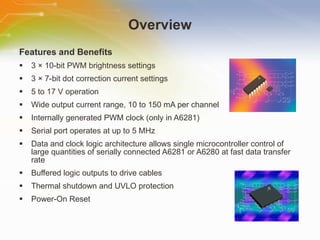
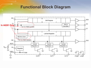
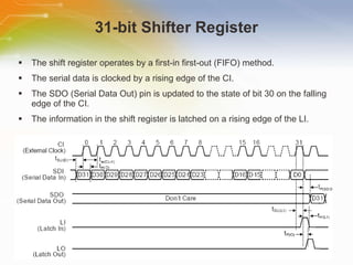
This document introduces the three-channel constant-current LED driver family from Allegro Microsystems, detailing its internal functions, features, and design considerations. Key features include programmable PWM control, various brightness and dot correction settings, and protection mechanisms like thermal shutdown and undervoltage lockout. It also outlines the operational parameters and design resources for the A6280 and A6281 LED driver models.


![5G Explained! A High Level Overview [Introduction]](https://cdn.slidesharecdn.com/ss_thumbnails/5gexplainedahighleveloverview-260119165306-cc137a3e-thumbnail.jpg?width=640&height=640&fit=bounds)


