What are the advantages and disadvantages of membrane structures.pptx
Peripheral 8245,16550&8237 dma controller
1. Peripheral 8245
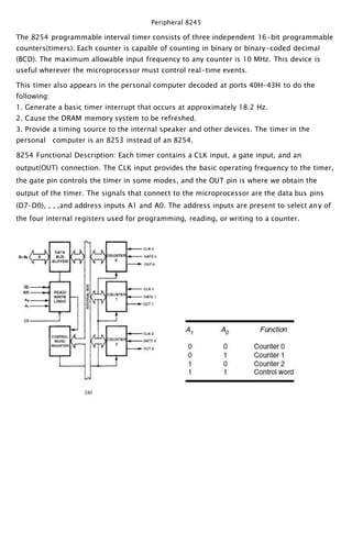
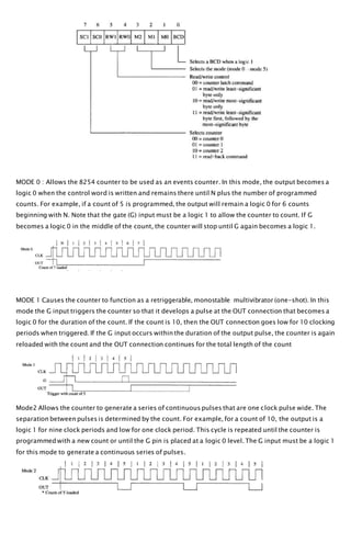
The 8254 programmable interval timer consists of three independent 16-bit programmable
counters(timers). Each counter is capable of counting in binary or binary-coded decimal
(BCD). The maximum allowable input frequency to any counter is 10 MHz. This device is
useful wherever the microprocessor must control real-time events.
This timer also appears in the personal computer decoded at ports 40H–43H to do the
following:
1. Generate a basic timer interrupt that occurs at approximately 18.2 Hz.
2. Cause the DRAM memory system to be refreshed.
3. Provide a timing source to the internal speaker and other devices. The timer in the
personal computer is an 8253 instead of an 8254.
8254 Functional Description: Each timer contains a CLK input, a gate input, and an
output(OUT) connection. The CLK input provides the basic operating frequency to the timer,
the gate pin controls the timer in some modes, and the OUT pin is where we obtain the
output of the timer. The signals that connect to the microprocessor are the data bus pins
(D7–D0), , , ,and address inputs A1 and A0. The address inputs are present to select any of
the four internal registers used for programming, reading, or writing to a counter.
2. MODE 0 : Allows the 8254 counter to be used as an events counter. In this mode, the output becomes a
logic 0 when the control word is written and remains there until N plus the number of programmed
counts. For example, if a count of 5 is programmed, the output will remain a logic 0 for 6 counts
beginning with N. Note that the gate (G) input must be a logic 1 to allow the counter to count. If G
becomes a logic 0 in the middle of the count, the counter will stop until G again becomes a logic 1.
MODE 1 Causes the counter to function as a retriggerable, monostable multivibrator (one-shot). In this
mode the G input triggers the counter so that it develops a pulse at the OUT connection that becomes a
logic 0 for the duration of the count. If the count is 10, then the OUT connection goes low for 10 clocking
periods when triggered. If the G input occurs within the duration of the output pulse, the counter is again
reloaded with the count and the OUT connection continues for the total length of the count
Mode2 Allows the counter to generate a series of continuous pulses that are one clock pulse wide. The
separation between pulses is determined by the count. For example, for a count of 10, the output is a
logic 1 for nine clock periods and low for one clock period. This cycle is repeated until the counter is
programmed with a new count or until the G pin is placed at a logic 0 level. The G input must be a logic 1
for this mode to generate a continuous series of pulses.
3. MODE 3 Generates a continuous square wave at the OUT connection, provided that the G pin is a logic 1.
If the count is even, the output is high for one half of the count and low for one half of the count. If the
count is odd, the output is high for one clocking period longer than it is low. For example, if the counter
is programmed for a count of 5, the output is high for three clocks and low for two clocks.
MODE 4 Allows the counter to produce a single pulse at the output. If the count is programmed as a 10,
the output is high for 10 clocking periods and low for one clocking period. The cycle does not begin until
the counter is loaded with its complete count. This mode operates as a software triggered oneshot.As
with modes 2 and 3, this mode also uses the G input to enable the counter. The G input must be a logic
1 for the counter to operate for these three modes.
MODE 5 A hardware triggered one-shot that functions as mode 4, except that it is started by a trigger
pulse on the G pin instead of by software. This mode is also similar to mode 1 because it is retriggerable.
Reading Counter: Each counter has an internal latch that is read with the read counter port
operation. These latches will normally follow the count. If the contents of the counter are
needed, then the latch can remember the count by programming the counter latch control
word which causes the contents of the counter to be held in a latch until they is read. When
it is necessary for the contents of more than one counter to be read at the same time, we
use the read-back control word, illustrated in Figure 11–38. With the read-back control
word, the bit is a logic 0 to cause the counters selected by CNT0, CNT1, and CNT2 to be
latched. If the status register is to be latched, then the bit is placed at a logic
4. The 16550 is a universal asynchronous receiver/transmitter (UART) that is fully compatible with the
Intel microprocessors. The 16550 is capable of operating at 0–1.5 M baud. Baud rate is the number of
bits transferred per second(bps), including start, stop, data, and parity (Bps is bytes per second and bps
are bits per second).The 16550 also includes a programmable baud rate generator and separate FIFOs for
input and output data to ease the load on the microprocessor. Each FIFO contains 16 bytes of
storage.This is the most common communications interface found in modem microprocessor-based
equipment.
Asynchronous serial data are transmitted and received without a clock or timing signal. Each frame
contains a start bit, seven data bits, parity, and one stop bit.
5. The contents of the 16550 line control register
The operation of the ST and parity bits
the baud rate=18.432 MHz/(16 × divisor value)
6. the divisor value=18.432 MHz ÷(16× baud rate)
An asynchronous system requires seven data bits, odd parity a baud rate of 9600, and one stop bit.Write
a procedure that initializes the 16550 to function in this manner.
Baud rate 9600, 7 data, odd parity, 1 stop
LINE EQU 0F3H
LSB EQU 0F0H
MSB EQU 0F1H
FIFO EQU 0F2H
START PROC NEAR
MOV AL,10001010B ;enable baud rate divisor
OUT LINE,AL
MOV AL,120 ;program baud 9600
OUT LSB,AL
MOV AL,0
OUT MSB,AL
MOV AL,00001010B ;program 7 data, odd
OUT LINE,AL ;parity, 1 stop
MOV AL,00000111B ;enable transmitter and
OUT FIFO,AL ;receiver
RET
START ENDP
Sending Serial Data: A procedure that transmits AH via the 16650 UART
LSTAT EQU 0F5H ;line status port
DATA EQU 0F0H ;data port
7. SEND PROC NEAR
PUSH AX ;save AX
IN AL,LSTAT ;get line status register
TEST AL,20H ;test TH bit
JZ SEND ;if transmitter not ready
MOV AL,AH ;get data
OUT DATA,AL ;transmit data
POP AX ;restore AX
RET
SEND ENDP
Receive Serial Data:A procedure that receives data from the 16550 UART and returns it in AL.
LSTAT EQU 0F5H ;line status port
DATA EQU 0F0H ;data port
RECV PROC NEAR
IN AL,LSTAT ;get line status register
TEST AL,1 ;test DR bit
JZ RECV ;if no data in receiver
TEST AL,0EH ;test all 3 error bits
JNZ ERR ;for an error
IN AL,DATA ;read data from 16550
RET
ERR:
MOV AL,’?’ ;get question mark
RET
RECV ENDP
UART Errors: The types of errors detected by the 16550 are parity error, framing error, and overrun error.
A parity error indicates that the received data contain the wrong parity. A framing error indicates that the
start and stop bits are not in their proper places. An overrun error indicates that data have overrun the
internal receiver FIFO buffer. These errors should not occur during normal operation. If a parity error
occurs, it indicates that noise was encountered during reception. A framing error occurs if the receiver is
receiving data at an incorrect baud rate. An overrun error occurs only if the software fails to read the data
from the UART before the receiver FIFO is full. This example does not test the BI (break indicator bit) for a
break condition. Note that a break is two consecutive frames of logic 0s on the SIN pin of the UART.
9. InternalRegisters
CAR The currentaddress register is used to hold the 16-bit memory address used forthe DMA
transfer. Each channel has its own current address registerfor this purpose.When a byte of data is transferred
during a DMA operation, the CAR is either incremented or decremented, depending on how it is programmed.
CWCR The currentword countregister programs a channel for the number of bytes (up to 64K)
transferred during a DMA action. The number loaded into this registeris one less than the number of bytes
transferred. For example, if a 10 is loaded into the CWCR,then 11 bytes are transferred during the DMA action.
BA and BWC The base address (BA)and base word count (BWC)registers are used when auto-initialization is
selected fora channel. In the auto-initialization mode,these registers are used to reload both the CAR and CWCR
after the DMA action is completed.This allows the same count and address to be used to transfer data from the
same memoryarea.