Downloaded 490 times
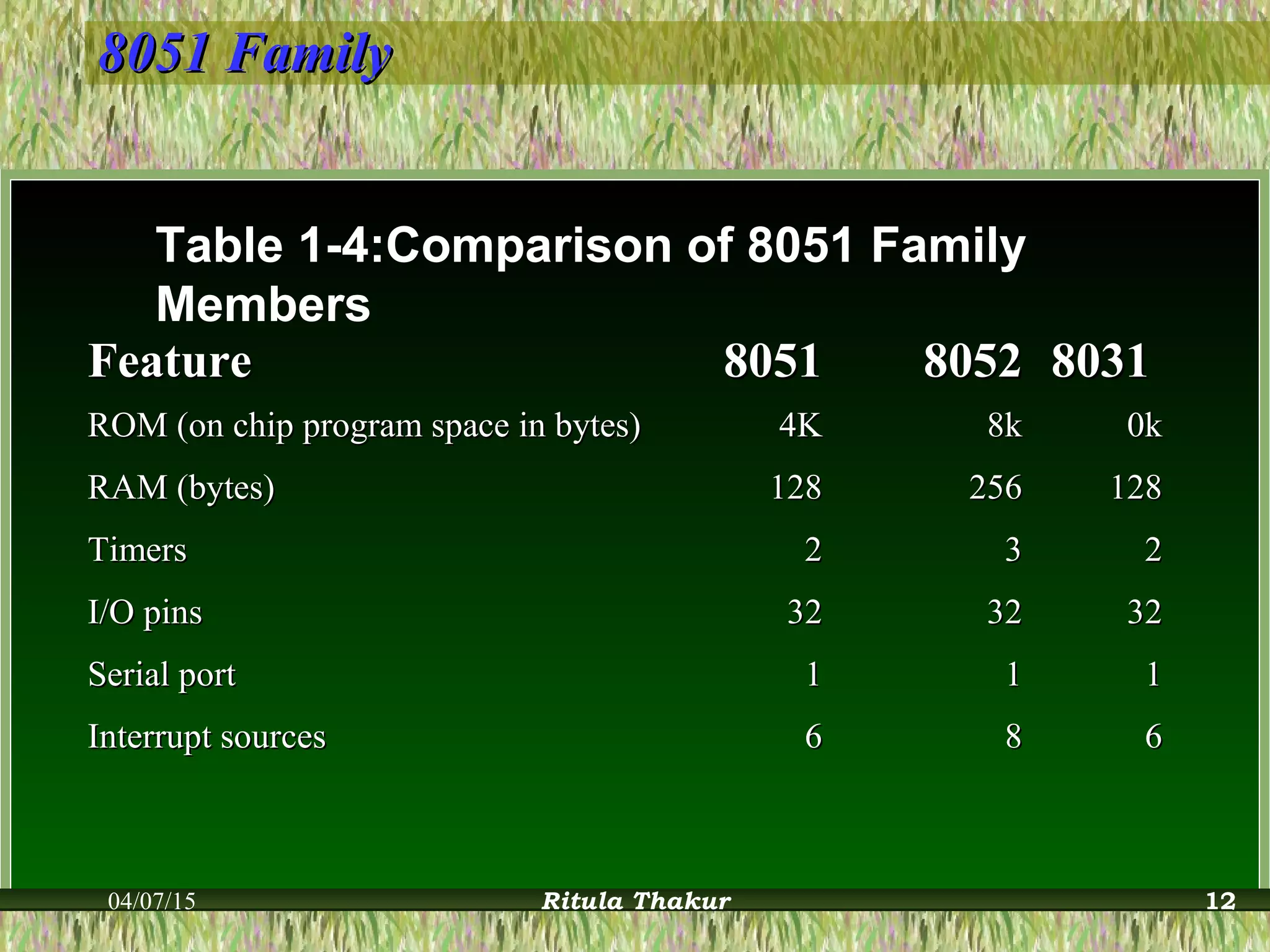
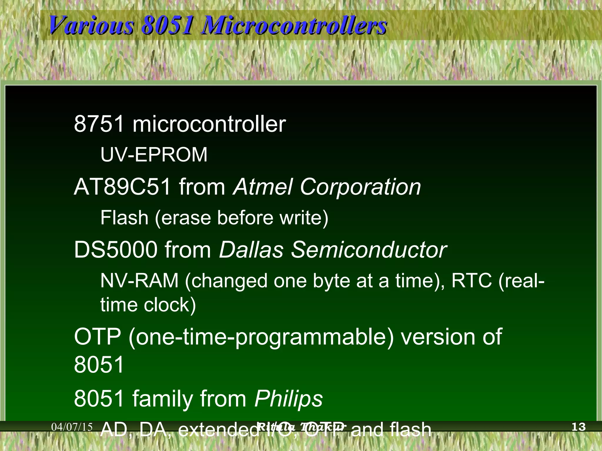
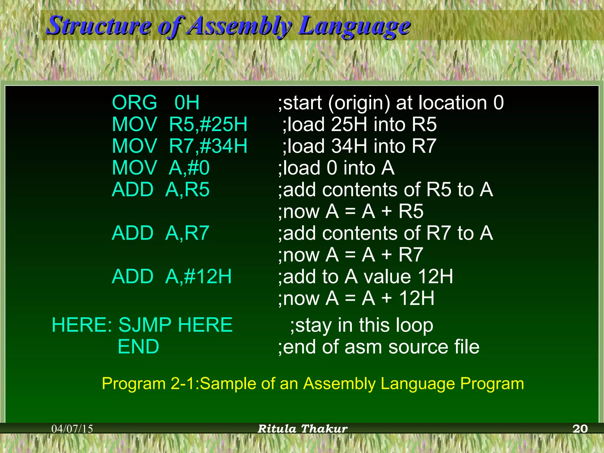
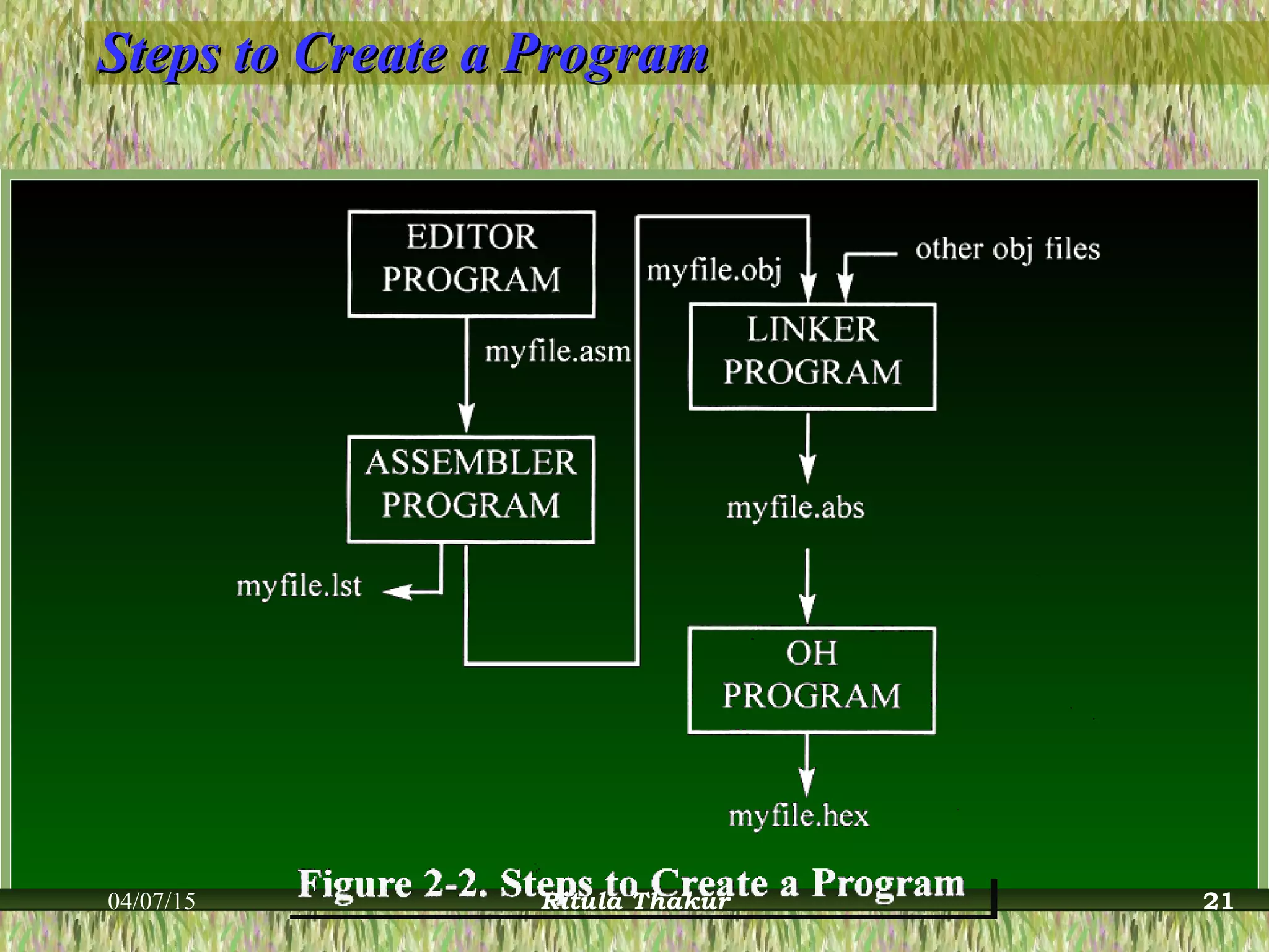
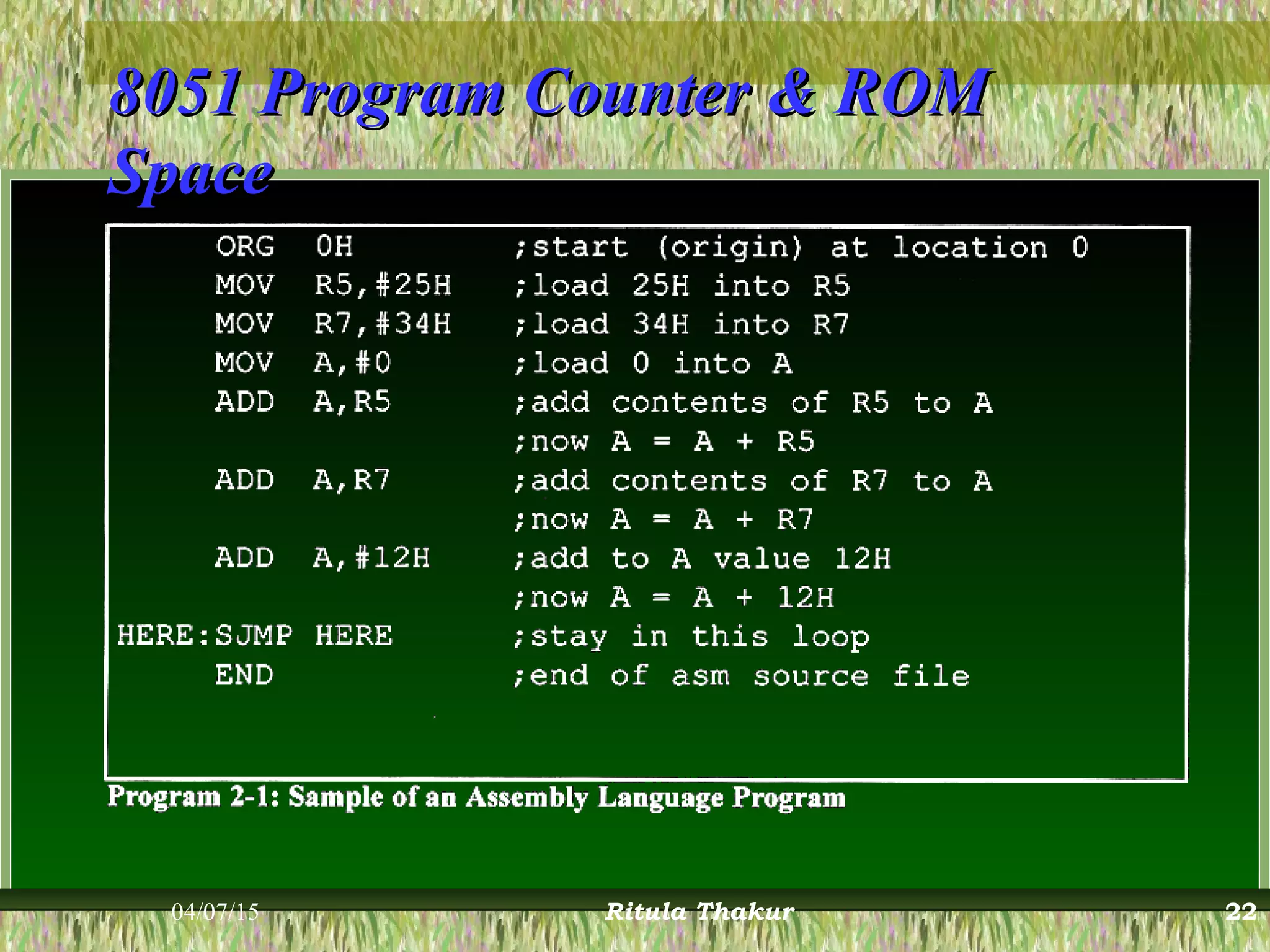
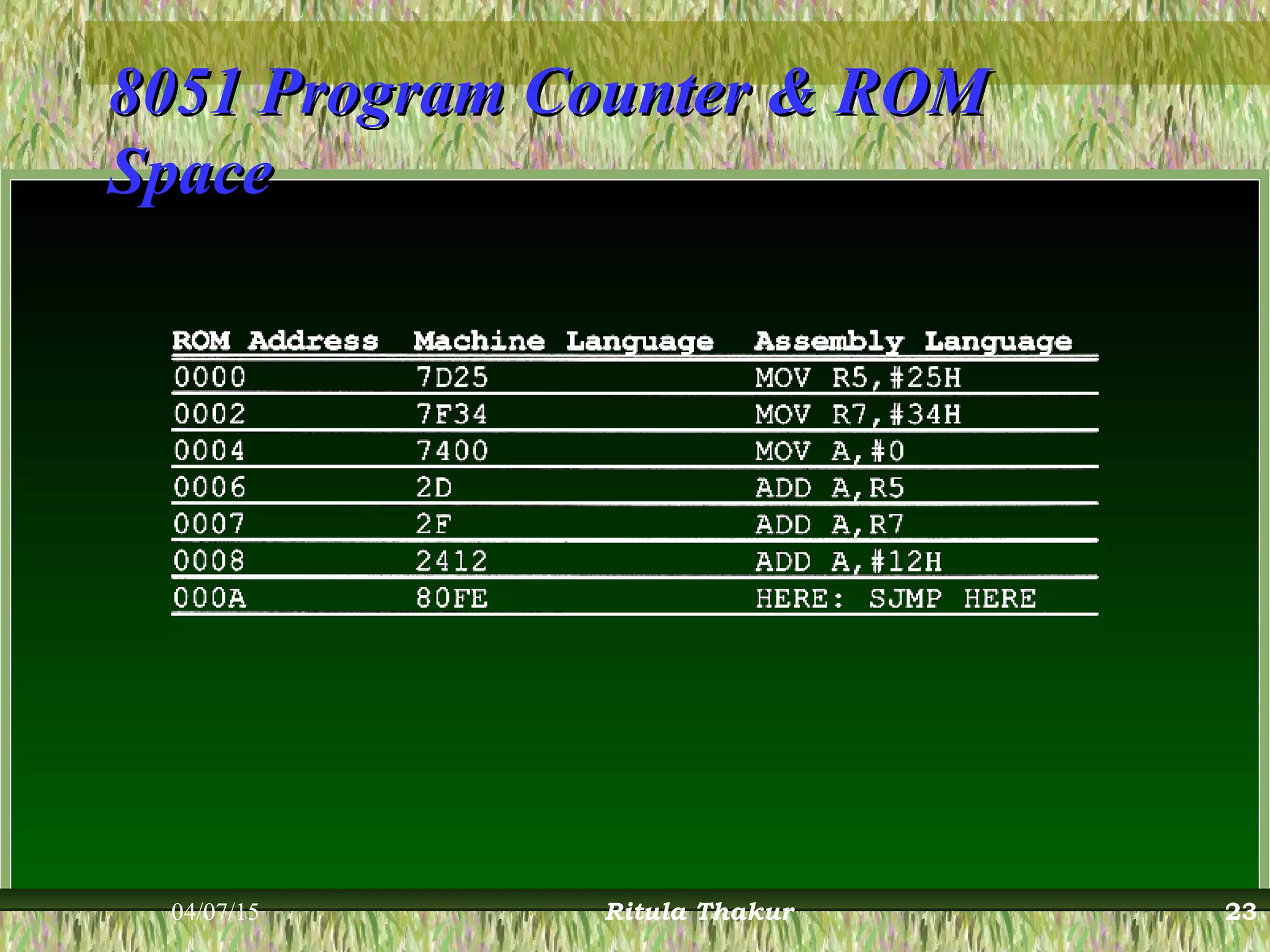


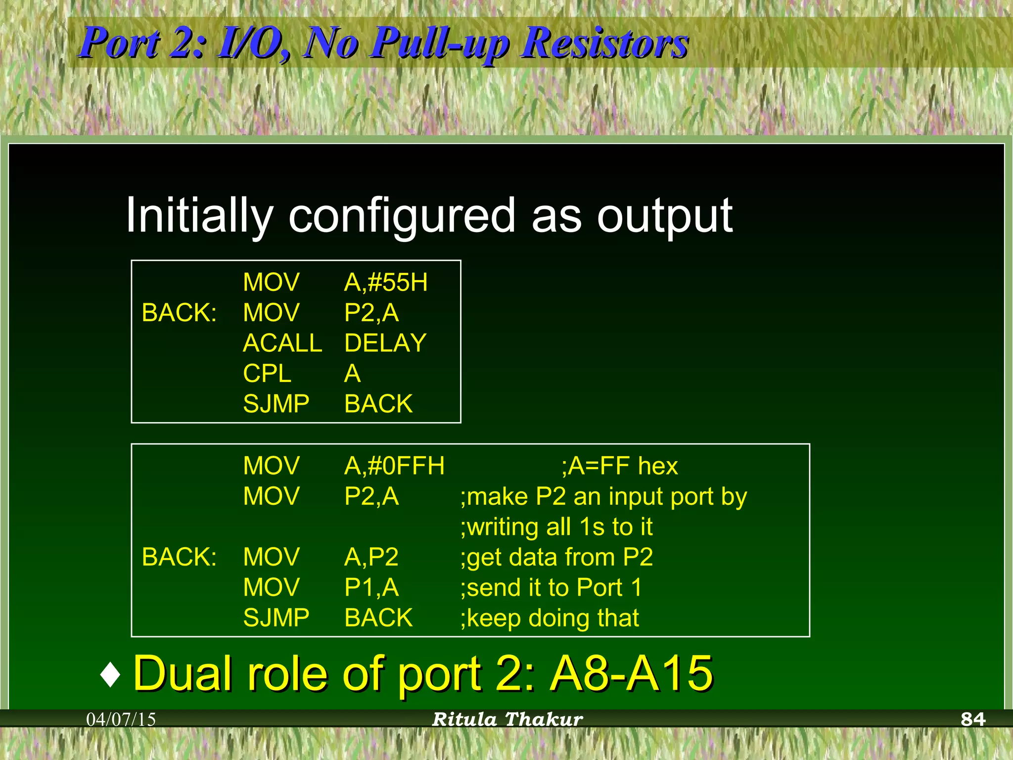
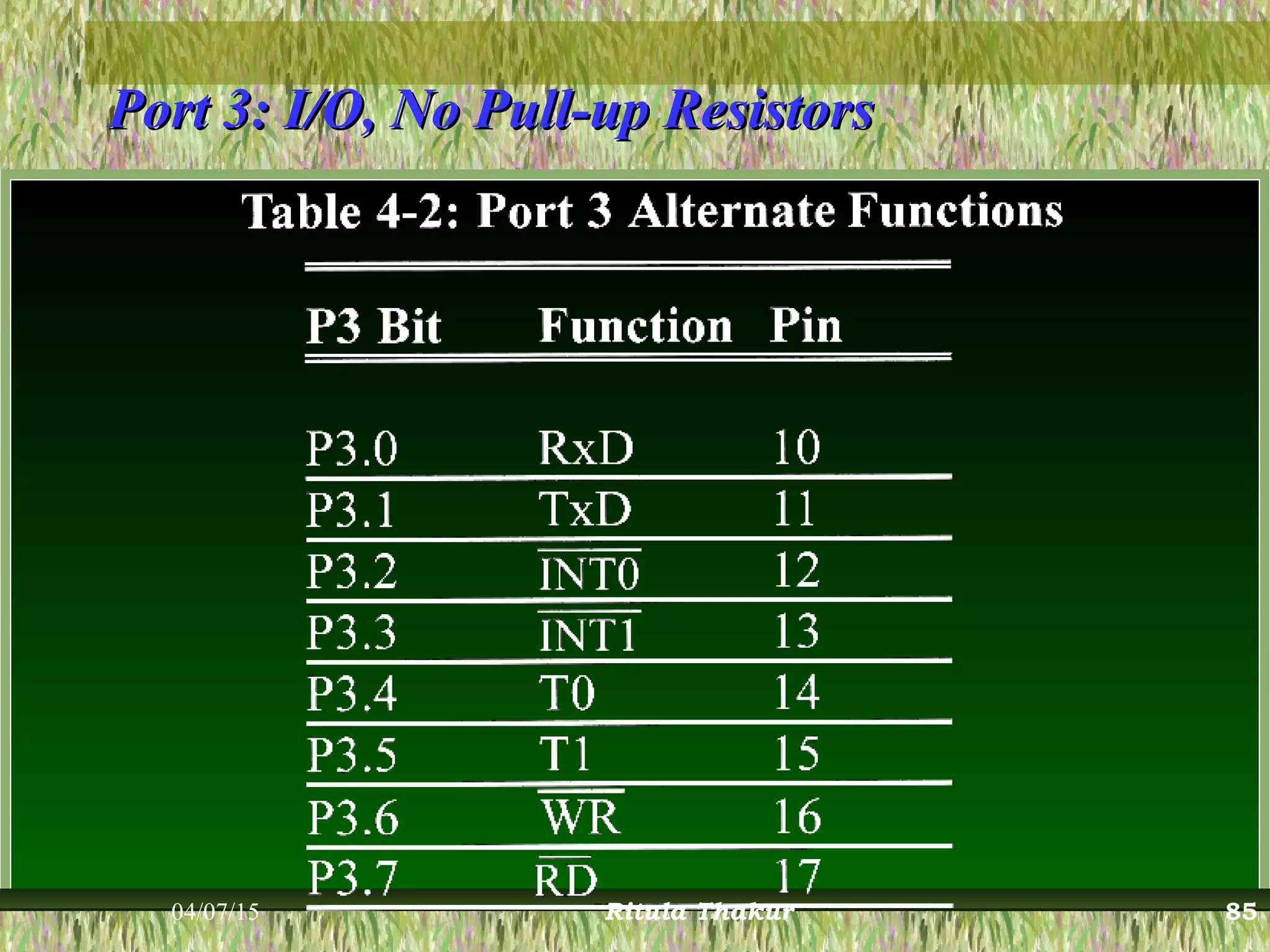
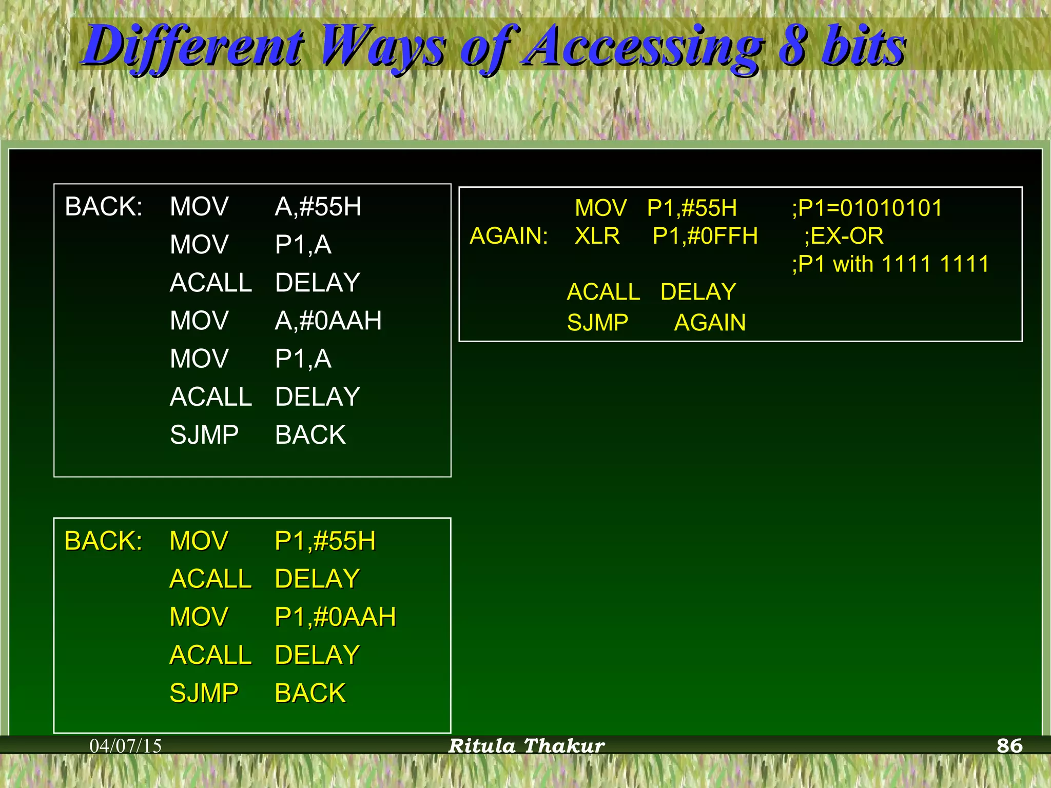
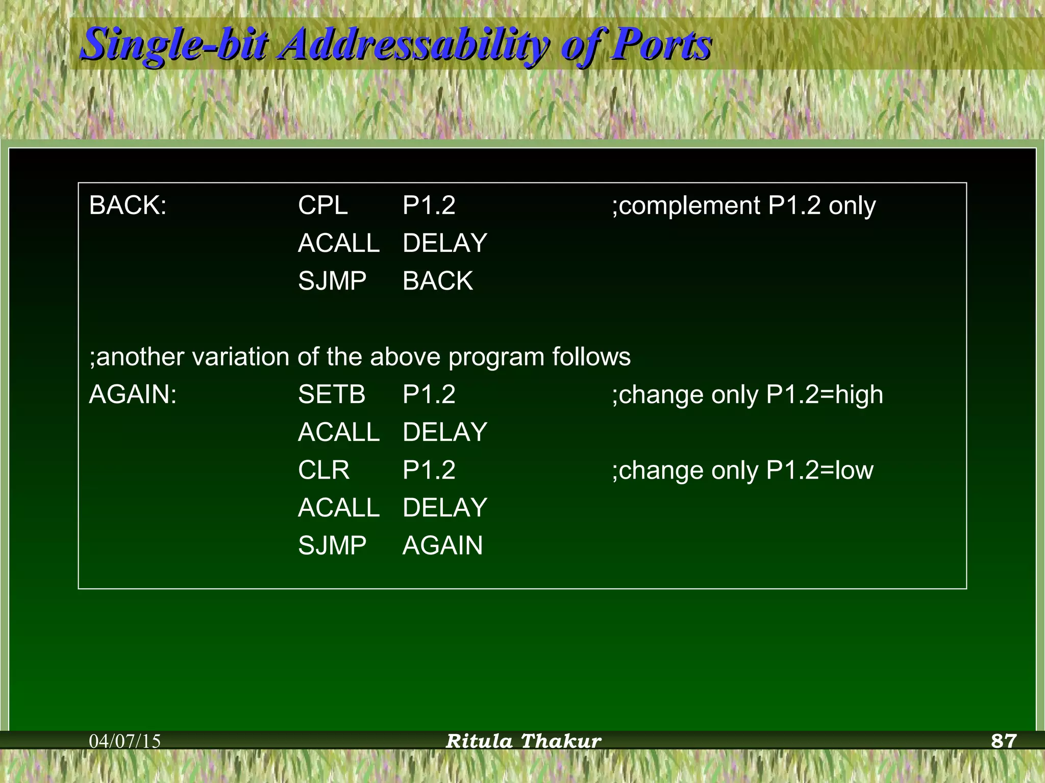

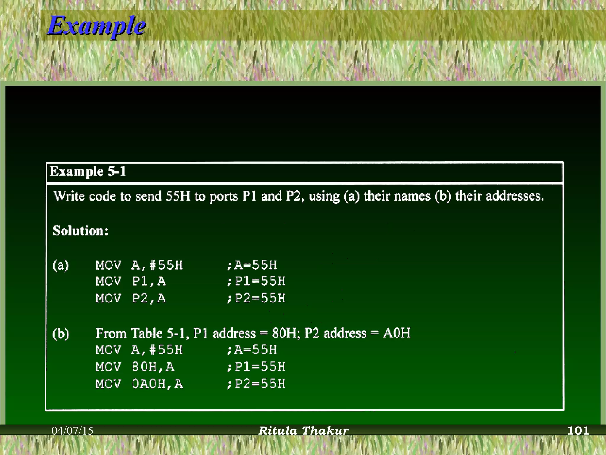
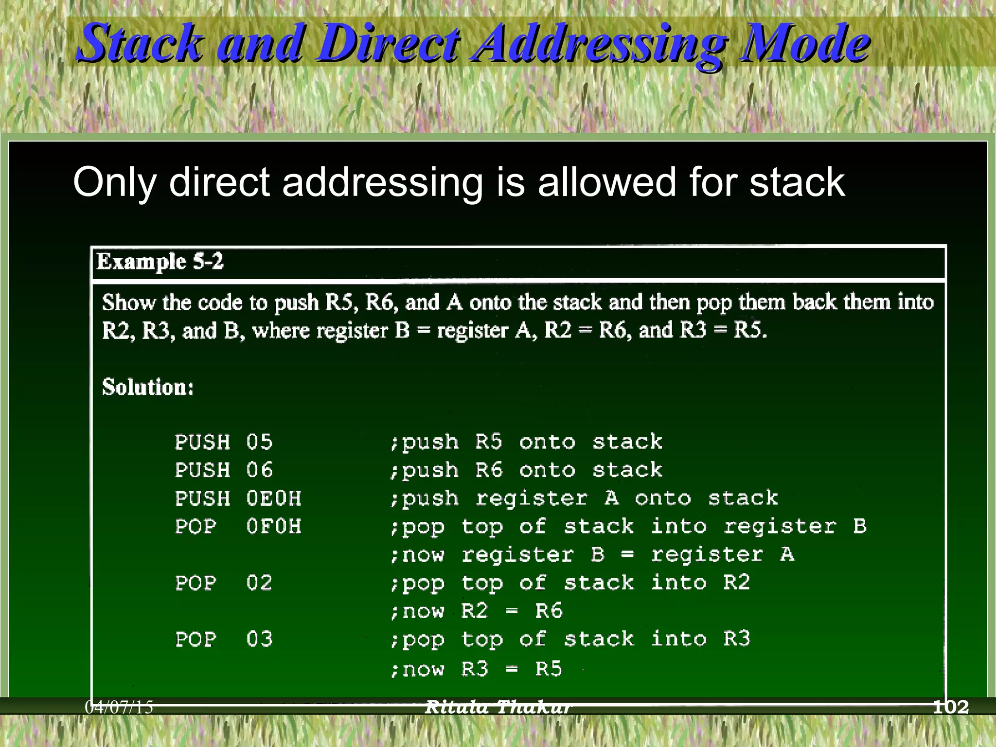
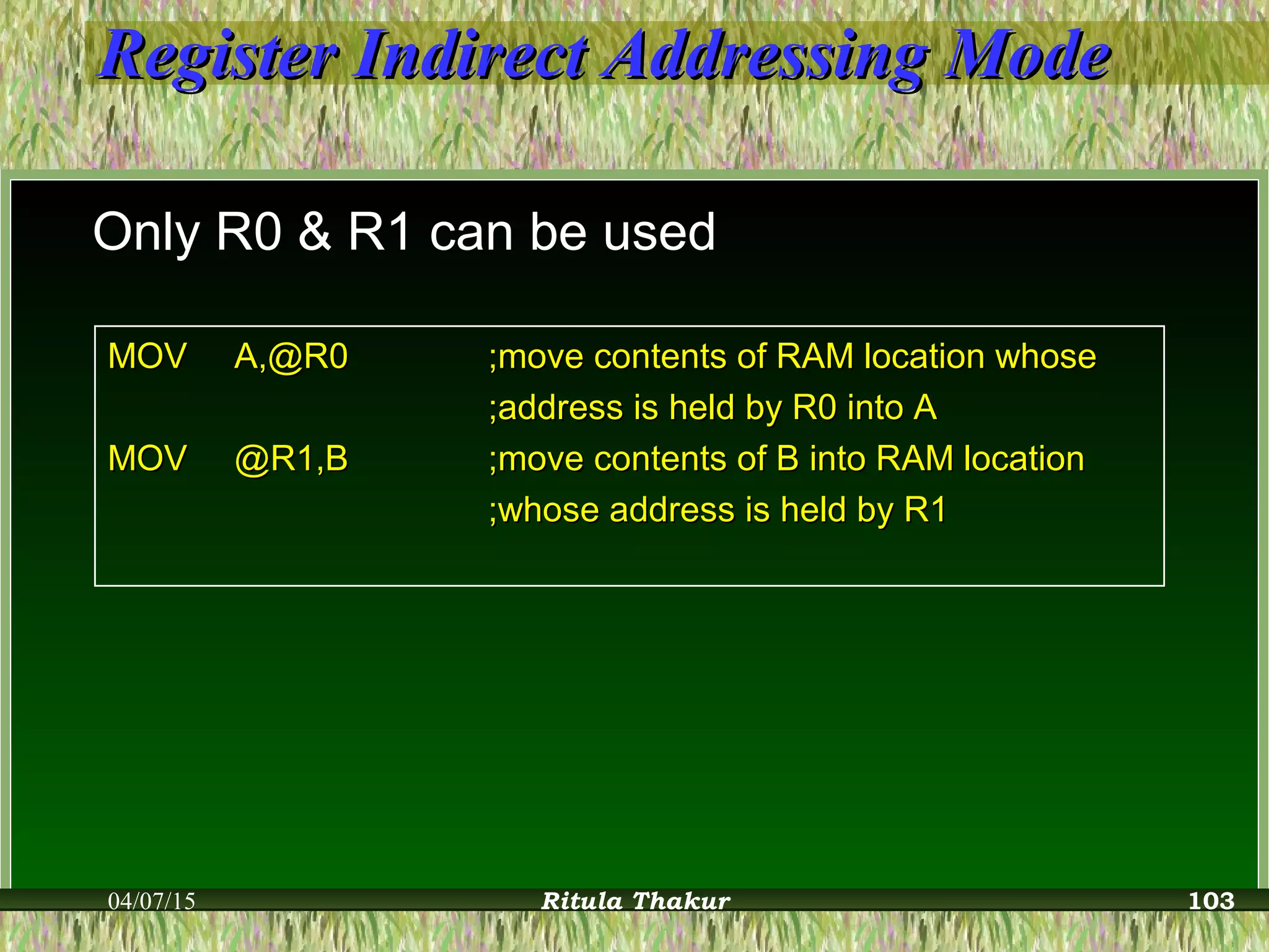
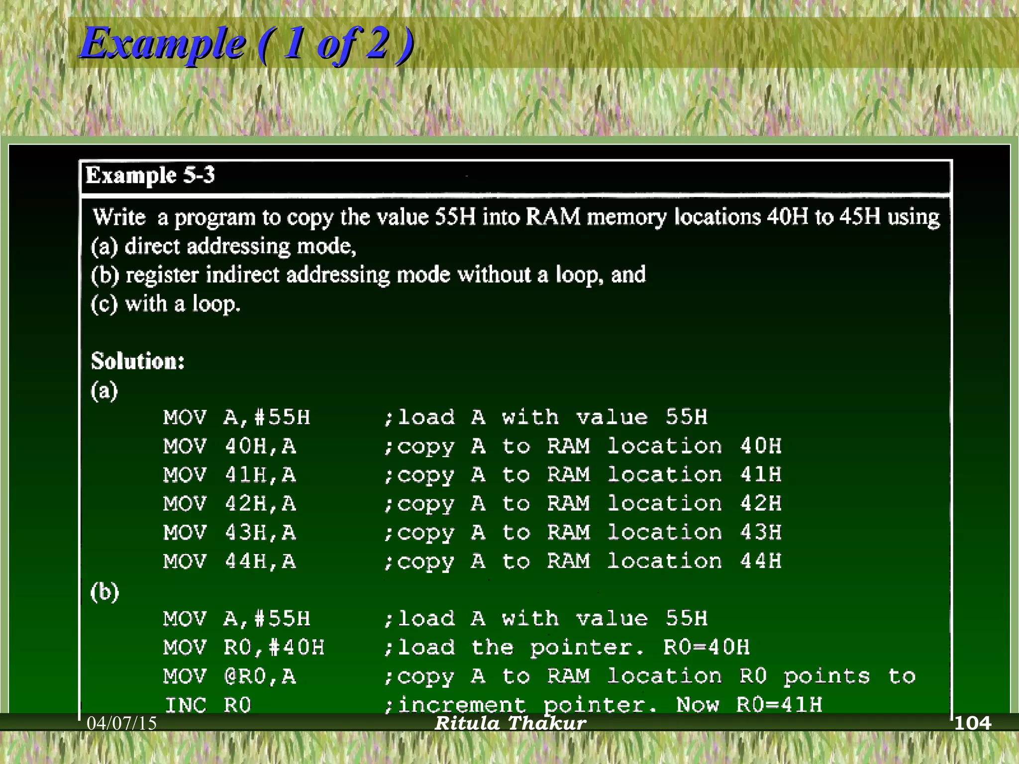

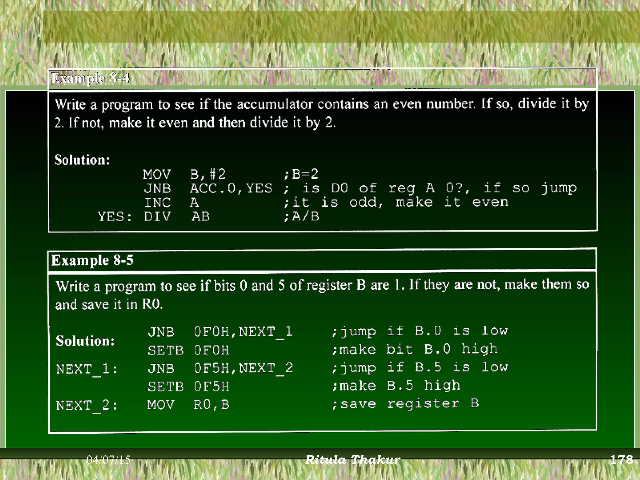
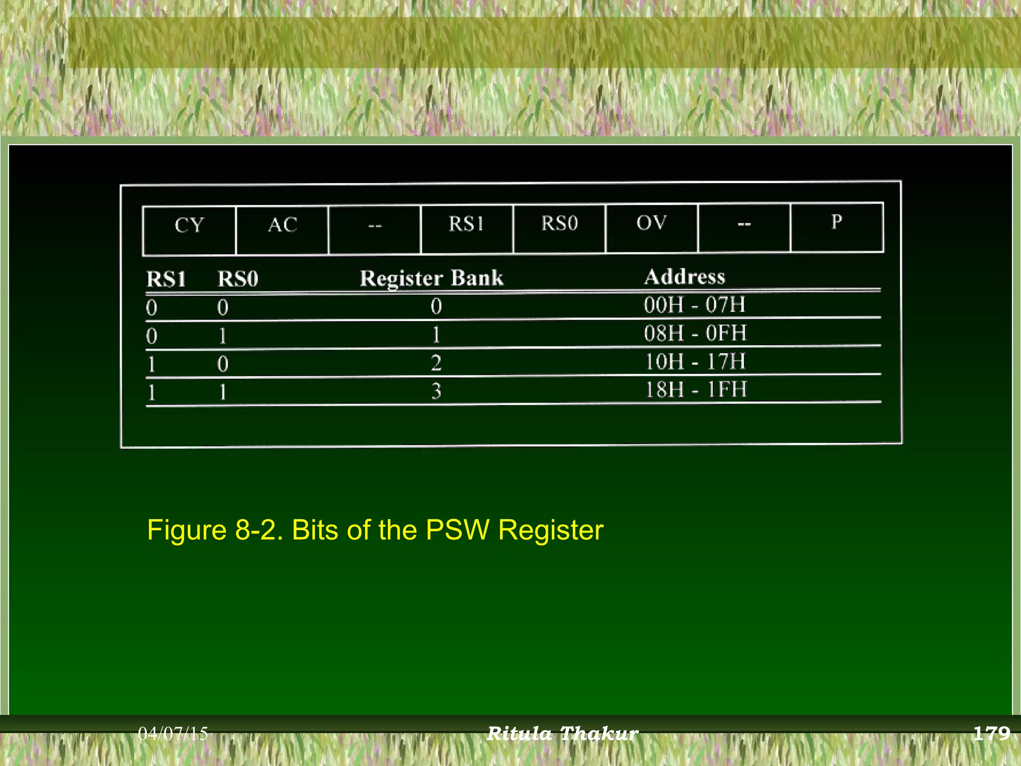
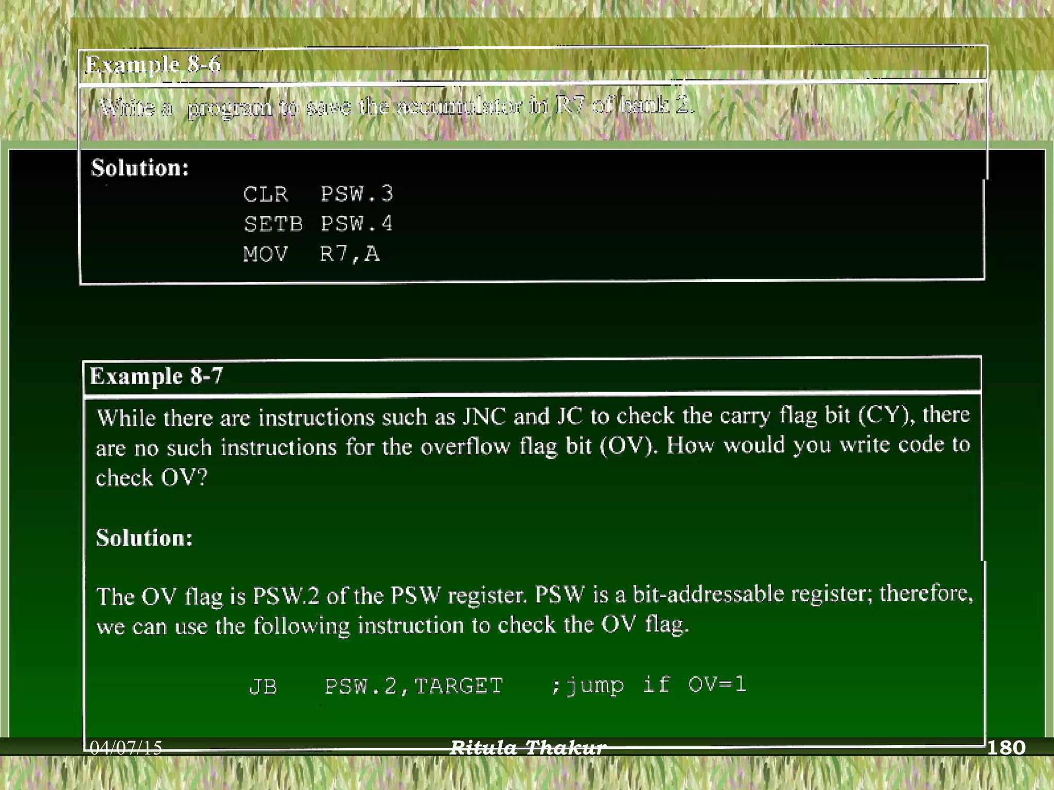
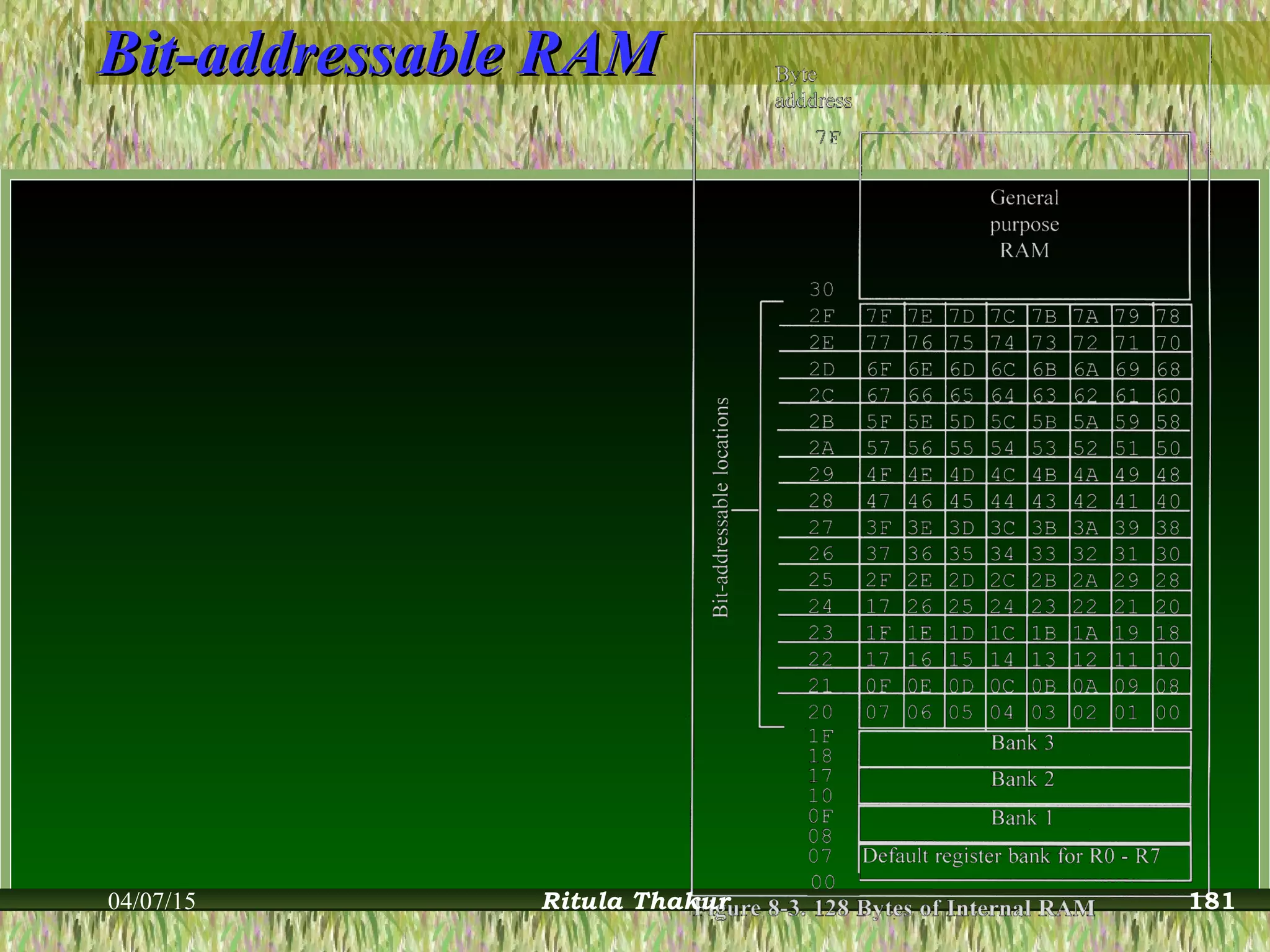
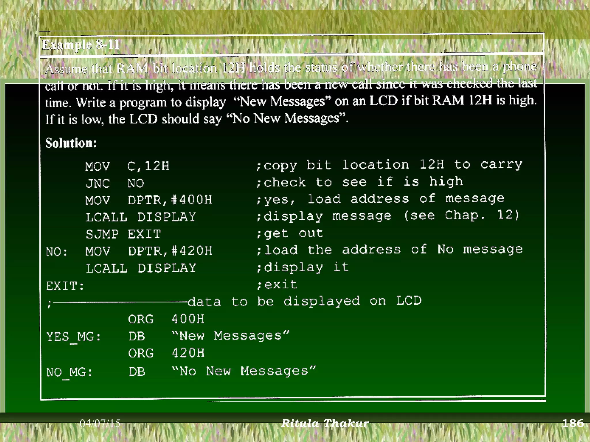
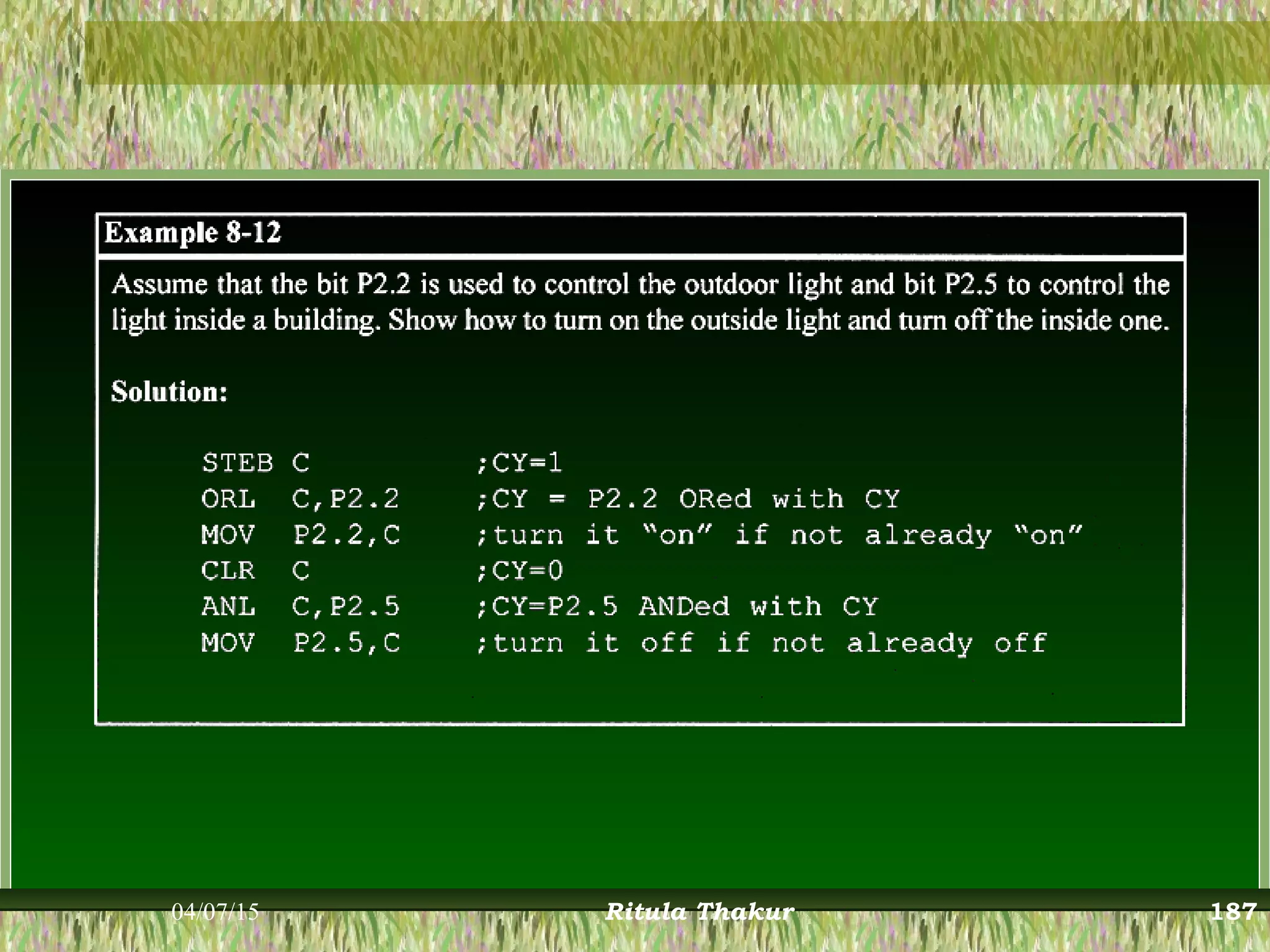
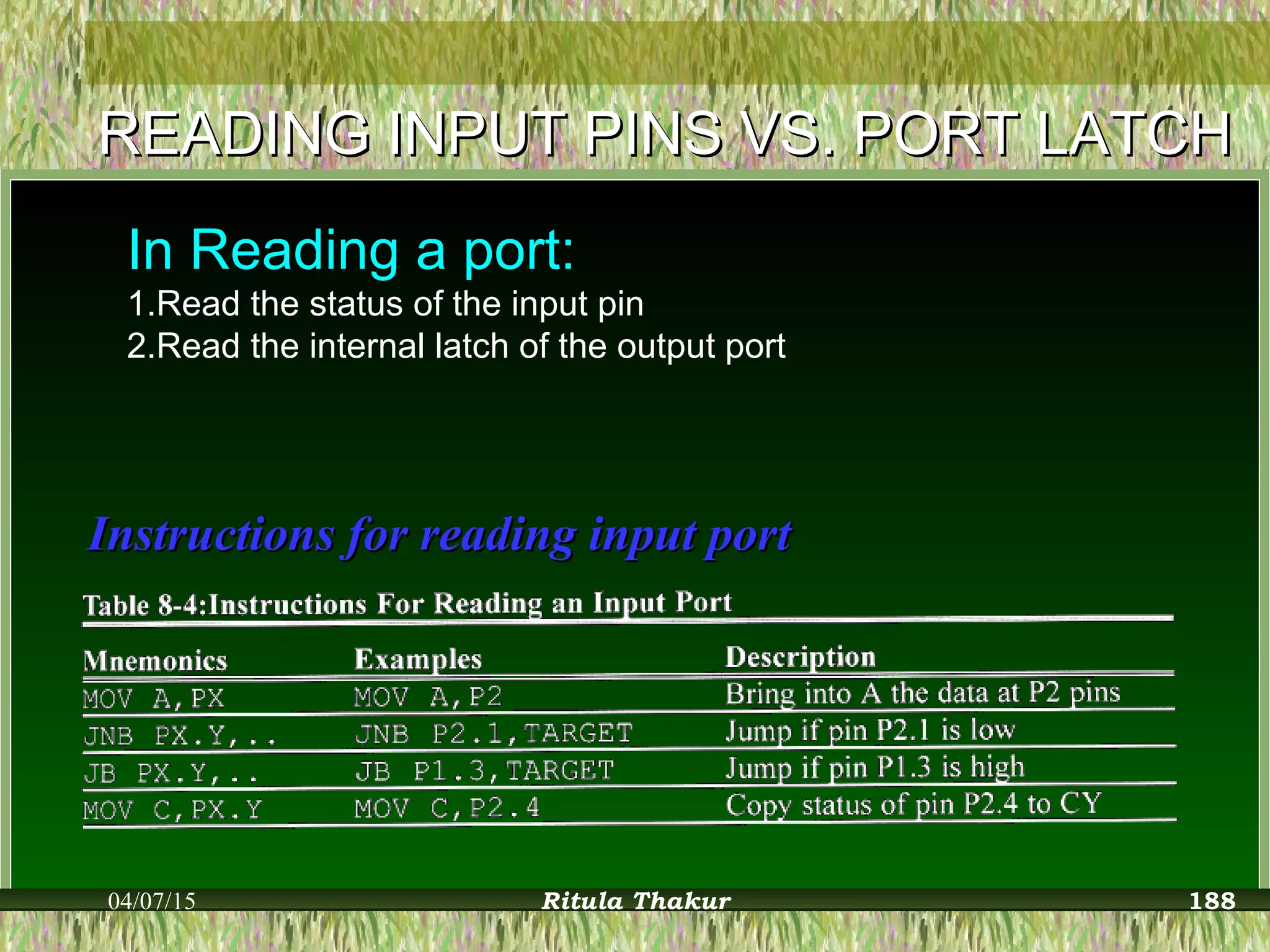
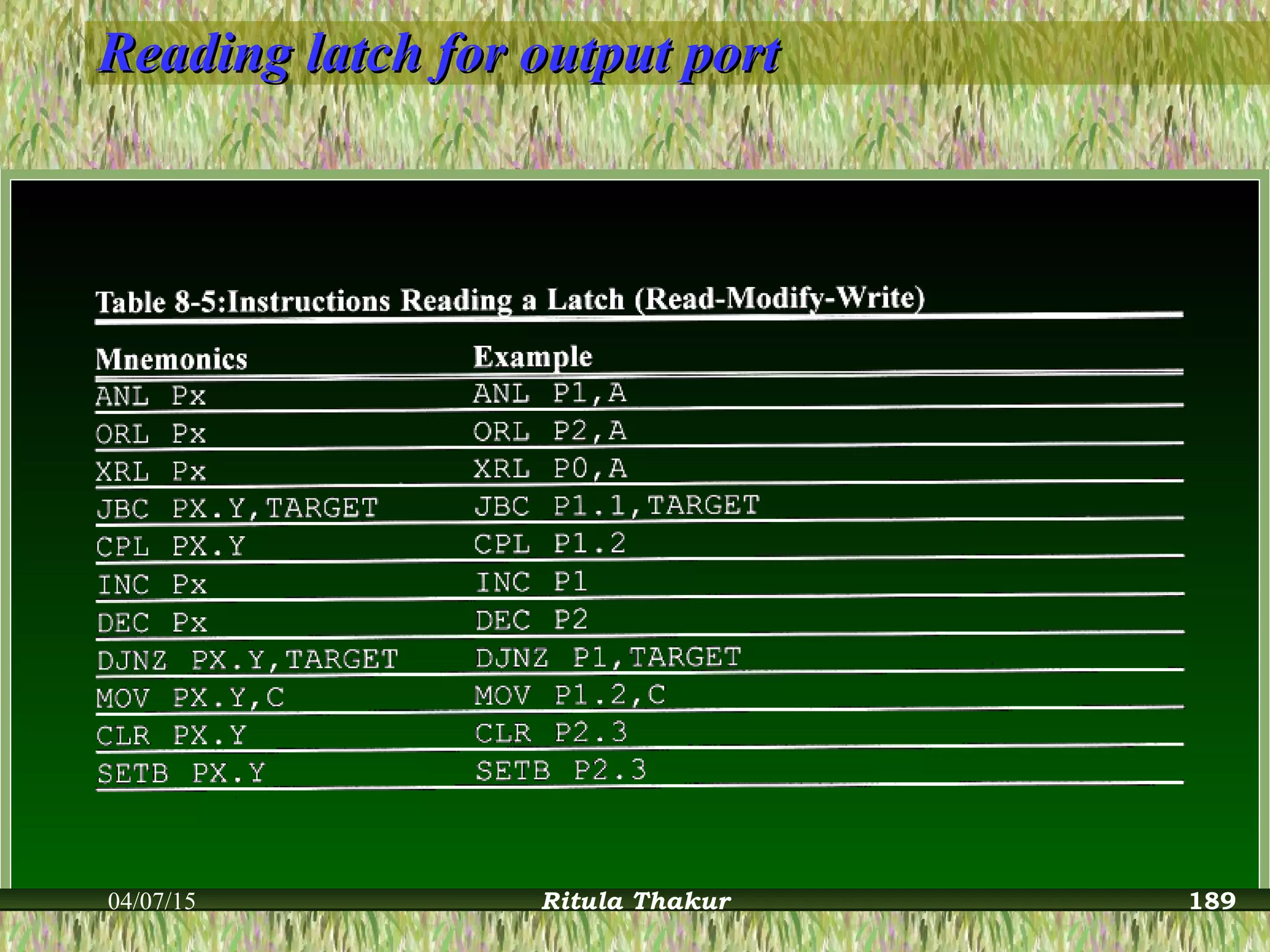
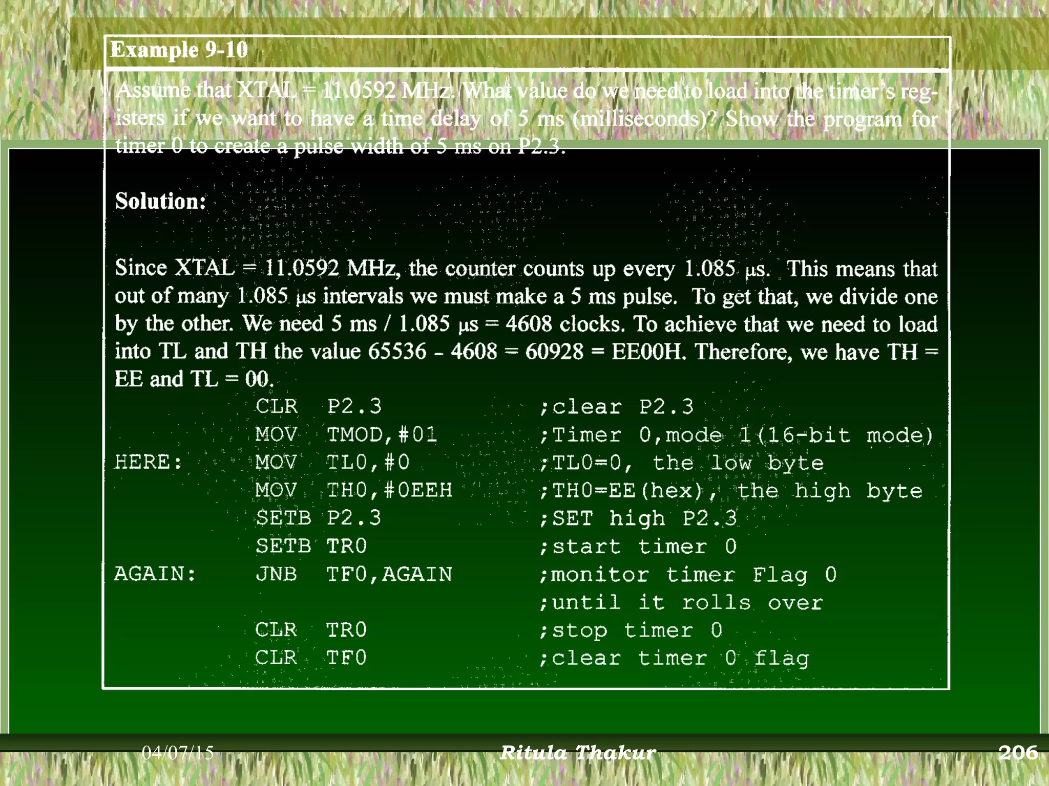


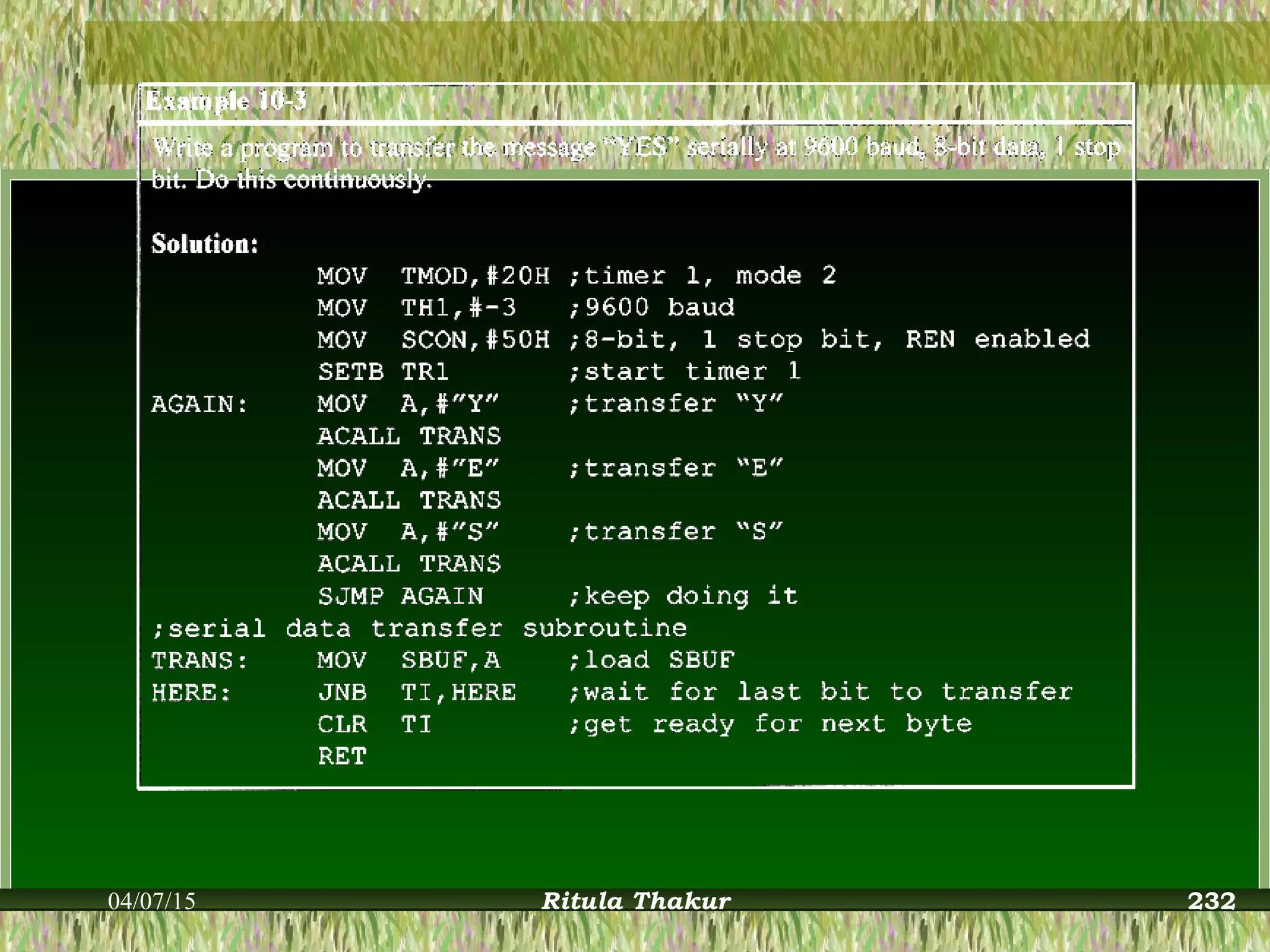
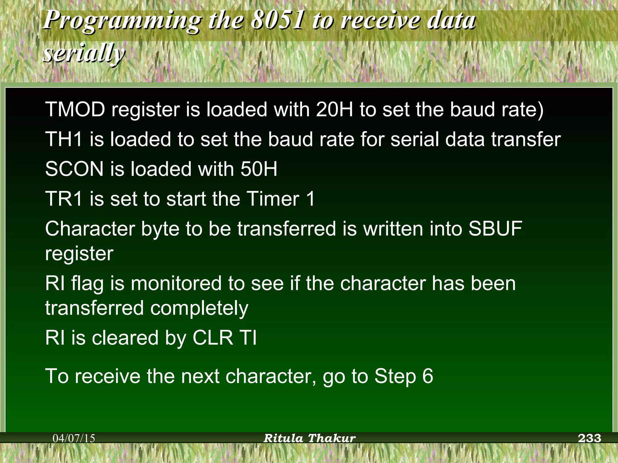
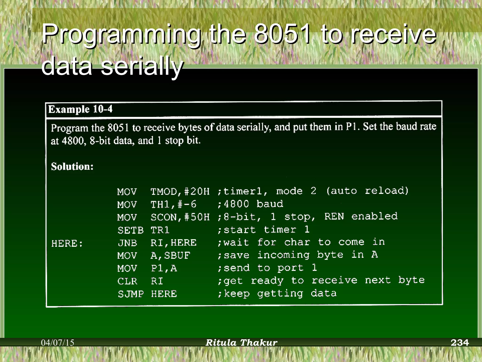
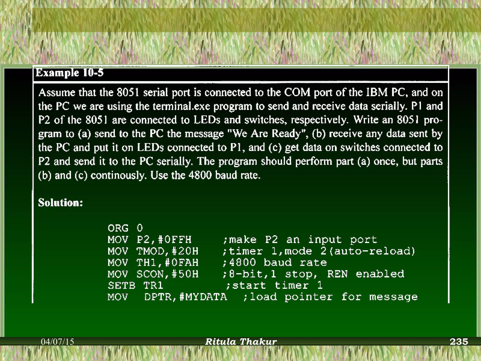


The document provides an overview of the 8051 microcontroller, comparing it with microprocessors and discussing its applications in embedded systems. It covers the features and advantages of various members of the 8051 family from different manufacturers, programming basics, and input/output port handling. Assembly language programming, including instructions and the structure of programs, is also detailed along with examples for better understanding.