Mpi lab manual eee
•Download as DOCX, PDF•
1 like•736 views

The document describes a lab manual for experiments with an 8085 microprocessor. It includes: 1) 13 assembly language programs to perform operations like data transfer, addition, comparison etc. using the 8085 microprocessor kit. 2) Details of the 8085 microprocessor architecture including registers, flags, pin descriptions. 3) Information about the memory map, I/O ports, and other integrated circuits used in the microprocessor kit like 8253, 8255, 8279. 4) Procedures for entering and executing programs on the microprocessor kit and expected input/output for programs. The document provides comprehensive information needed to learn and perform various experiments on an 8085 microprocessor

Recommended
More Related Content
What's hot
What's hot (20)
Similar to Mpi lab manual eee
Similar to Mpi lab manual eee (20)
More from Vivek Kumar Sinha
More from Vivek Kumar Sinha (20)
Recently uploaded
Recently uploaded (20)
Mpi lab manual eee
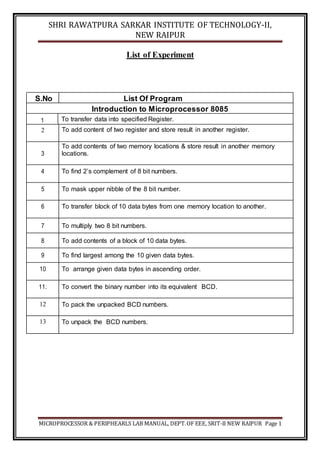
- 1. SHRI RAWATPURA SARKAR INSTITUTE OF TECHNOLOGY-II, NEW RAIPUR MICROPROCESSOR & PERIPHEARLS LAB MANUAL, DEPT.OF EEE, SRIT-II NEW RAIPUR Page 1 List of Experiment S.No List Of Program Introduction to Microprocessor 8085 1 To transfer data into specified Register. 2 To add content of two register and store result in another register. 3 To add contents of two memory locations & store result in another memory locations. 4 To find 2’s complement of 8 bit numbers. 5 To mask upper nibble of the 8 bit number. 6 To transfer block of 10 data bytes from one memory location to another. 7 To multiply two 8 bit numbers. 8 To add contents of a block of 10 data bytes. 9 To find largest among the 10 given data bytes. 10 To arrange given data bytes in ascending order. 11. To convert the binary number into its equivalent BCD. 12 To pack the unpacked BCD numbers. 13 To unpack the BCD numbers.
- 2. SHRI RAWATPURA SARKAR INSTITUTE OF TECHNOLOGY-II, NEW RAIPUR MICROPROCESSOR & PERIPHEARLS LAB MANUAL, DEPT.OF EEE, SRIT-II NEW RAIPUR Page 2 INTRODUCTION TO MICROPROCESSOR 8085 Architecture of 8085 Microprocessor a) General purpose register It is an 8 bit register i.e. B,C,D,E,H,L. The combination of 8 bit register is known as register pair, which can hold 16 bit data. The HL pair is used to act as memory pointer is accessible to program. b) Accumulator It is an 8 bit register which hold one of the data to be processed by ALU and stored the result of the operation. c) Program counter (PC) It is a 16 bit pointer which maintain the address of a byte entered to line stack. d) Stack pointer (Sp) It is a 16 bit special purpose register which is used to hold line memory address for line next instruction to be executed. e) Arithmetic and logical unit It carries out arithmetic and logical operation by 8 bit address it uses the accumulator content as input the ALU result is stored back into accumulator. f) Temporary register It is an 8 bit register associated with ALU hold data, entering an operation, used by the microprocessor and not accessible to programs. g) Flags Flag register is a group of fire, individual flip flops line content of line flag register will change after execution of arithmetic and logic operation. The line states flags are i) Carry flag (C) ii) Parity flag (P) iii) Zero flag (Z) iv) Auxiliary carry flag (AC) v) Sign flag (S) h) Timing and control unit Synchronous all microprocessor, operation with the clock and generator and control signal from it necessary to communicate between controller and peripherals. i) Instruction register and decoder Instruction is fetched from line memory and stored in line instruction register decoder the stored information. j) Register Array These are used to store 8 bit data during execution of some instruction.
- 3. SHRI RAWATPURA SARKAR INSTITUTE OF TECHNOLOGY-II, NEW RAIPUR MICROPROCESSOR & PERIPHEARLS LAB MANUAL, DEPT.OF EEE, SRIT-II NEW RAIPUR Page 3 PIN Description Address Bus 1. The pins Ao – A15 denote the address bus. 2. They are used for most significant bit Address / Data Bus 1. AD0 – AD7 constitutes the address / Data bus 2. These pins are used for least significant bit ALE : (Address Latch Enable) 1. The signal goes high during the first clock cycle and enables the lower order address bits. IO / M 1. This distinguishes whether the address is for memory or input. 2. When this pins go high, the address is for an I/O device. S0 – S1 S0 and S1 are status signal which provides different status and functions. RD 1. This is an active low signal 2. This signal is used to control READ operation of the microprocessor. WR 1. WR is also an active low signal 2. Controls the write operation of the microprocessor. HOLD 1. This indicates if any other device is requesting the use of address and data bus. HLDA 1. HLDA is the acknowledgement signal for HOLD 2. It indicates whether the hold signal is received or not. INTR 1. INTE is an interrupt request signal 2. IT can be enabled or disabled by using software INTA 1. Whenever the microprocessor receives interrupt signal 2. It has to be acknowledged. RST 5.5, 6.5, 7.5 1. These are nothing but the restart interrupts 2. They insert an internal restart junction automatically.
- 4. SHRI RAWATPURA SARKAR INSTITUTE OF TECHNOLOGY-II, NEW RAIPUR MICROPROCESSOR & PERIPHEARLS LAB MANUAL, DEPT.OF EEE, SRIT-II NEW RAIPUR Page 4 TRAP 1. Trap is the only non-maskable interrupt 2. It cannot be enabled (or) disabled using program. RESET IN 1. This pin resets the program counter to 0 to 1 and results interrupt enable and HLDA flip flops. X1, X2 These are the terminals which are connected to external oscillator to produce the necessary and suitable clock operation. SID This pin provides serial input data SOD This pin provides serial output data VCC and VSS 1. VCC is +5V supply pin 2. VSS is ground pin Specifications 1. Processors Intel 8085 at E144 MHz clock 2. Memory Monitor RAM: 0000– IFFF EPROM Expansion: 2000– 3FFF’s 0000– FFF System RAM: 4000– 5FFF Monitor data area 4100– 5FFF RAM Expansion 6000– BFFF 3. Input / Output Parallel: A8 TTL input timer with 2 number of 32-55 only input timer available in -85 EBI. Serial: Only one number RS 232-C, Compatible, crucial interface using 8281A Timer: 3 channel -16 bit programmable units, using 8253 channel ‘0’ used for no band late. Clock generator. Channel ‘1’ is used for single stopping used program. Display: 6 digit – 7 segment LED display with filter 4 digit for adder display and 2 digit for data display. Key board: 21 keys, soft keyboard including common keys and hexa decimal keys. RES: Reset keys allow to terminate any present activity and retain to - 85 its on initialize state.
- 5. SHRI RAWATPURA SARKAR INSTITUTE OF TECHNOLOGY-II, NEW RAIPUR MICROPROCESSOR & PERIPHEARLS LAB MANUAL, DEPT.OF EEE, SRIT-II NEW RAIPUR Page 5 INT: Maskable interrupt connect to CPU’s RST 7.5 interrupt DEC: Decrement the adder by 1 EXEC: Execute line particular value after selecting address through go command. NEXT: Increment the address by 1 and then display its content. IC’s Used 8085 - 8 bit p 8253 - programmable internal timer 8255 - programmable peripheral interface 8279 - program mable key boards / display interface 8251 - programmable communication interface 2764 - 8 KV VV EPROM 6264 - 8K STATIC PROM 7414 - Hex inverter 7432 - Quad 21/p OR GATE 7409 - Quad 21/p AND GATE 7400 - NAND Gate 7404 - Dual D-FF 74373 - Octal ‘D’ Latch 74139 - Dual 2 to 4 line decoder 74138 - 3 to 8 line decoder In Enter Program into Trainer Kit 1. Press ‘RESET’ key 2. Sub (key processor represent address field) 3. Enter the address (16 bit) and digit in hex 4. Press ‘NEXT’ key 5. Enter the data 6. Again press “NEXT” 7. Again after taking the program, are use HLT instruction its Hex code 8. Press “NEXT” How to executive program 1. Press “RESET” 2. Press “GO” 3. Enter the address location in which line program was executed 4. Press “Execute” key
- 6. SHRI RAWATPURA SARKAR INSTITUTE OF TECHNOLOGY-II, NEW RAIPUR MICROPROCESSOR & PERIPHEARLS LAB MANUAL, DEPT.OF EEE, SRIT-II NEW RAIPUR Page 6 PROGRAM 1 Aim: To write an assembly language for transfer data into specified register. Apparatus required: 8085 micro processor kit (0-5V) DC battery Algorithm: Suppose data s are 20 and 30 Step1 : MOV A, 20 H Step2 : MOV B, 30 H Step3 : MOV C,A Step4 : MOV D, B. Step5 : HLT OUTPUT: Before Execution: A= 20; B= 30 After Execution: C= 20; D=30
- 7. SHRI RAWATPURA SARKAR INSTITUTE OF TECHNOLOGY-II, NEW RAIPUR MICROPROCESSOR & PERIPHEARLS LAB MANUAL, DEPT.OF EEE, SRIT-II NEW RAIPUR Page 7 PROGRAM 2 Aim: To write an assembly language for adding two 8 bit numbers by using micro processor kit. Apparatus required: 8085 micro processor kit (0-5V) DC battery Algorithm: Step1 : Start the microprocessor Step2 : Intialize the carry as ‘Zero’ Step3 : Load the first 8 bit data into the accumulator Step4 : Copy the contents of accum ulator into the register ‘B’ Step5 : Load the second 8 bit data into the accumulator. Step6 : Add the 2 - 8 bit datas and check for carry. Step7 : Jump on if no carry Step8 : Increment carry if there is Step9 : Store the added request in accumulator Step10 : More the carry value to accumulator Step11 : Store the carry value in accumulator Step12 : Stop the program execution. Address Label Mnemonics Hex Code Comments 4100 MVI C,00 OE, 00 Initialize the carry as zero 4102 LDA 4300 3A, (00, 43) Load the first 8 bit data 4105 MOV, B,A 47 Copy the value of 8 bit data into register B 4106 LDA 4301 3A, (01, 43) Load the second 8 bit data into the accumulator 4109 ADD B 80 Add the hoo values 410A JNC D2, 0E, 41 Jump on if no carry 410D INR C OC If carry is there increment it by one 410E Loop STA 4302 32 (02, 43) Stone the added value in the accumulator 4111 MOV A,C 79 More the value of carry to the accumulator from register C 4112 STA 4303 32 (03, 43) Store the value of carry in the accumulator 4115 HLT 76 Stop the program execution
- 8. SHRI RAWATPURA SARKAR INSTITUTE OF TECHNOLOGY-II, NEW RAIPUR MICROPROCESSOR & PERIPHEARLS LAB MANUAL, DEPT.OF EEE, SRIT-II NEW RAIPUR Page 8 Input Without carry Input Address Value 4300 04 4301 02 Output Output Address Value 4302 06 4303 00 (carry) With carry Input Address Value 4300 FF 4301 FF Output Address Value 4302 FE 4303 01 (carry) Calculation 1111 1111 1111 1111 --------------- (1) 1111 1110 ========= F E Result: The assembly language program for 8 bit addition of two numbers was executed successfully by using 8085 micro processing kit.
- 9. SHRI RAWATPURA SARKAR INSTITUTE OF TECHNOLOGY-II, NEW RAIPUR MICROPROCESSOR & PERIPHEARLS LAB MANUAL, DEPT.OF EEE, SRIT-II NEW RAIPUR Page 9 PROGRAM 3 Aim: To write an assembly language to add contents of two memory locations and store result in another memory locations. Add the contents of memory locations 4000H and 4001H and place the result in memory location 4002H. Apparatus required: 8085 micro processor kit (0-5V) DC battery Program: (4000H) = 14H (4001H) = 89H Result = 14H + 89H = 9DH Source program LXI H 4000H : HL points 4000H MOV A, M : Get first operand INX H : HL points 4001H ADD M : Add second operand INX H : HL points 4002H MOV M, A : Store result at 4002H HLT : Term inate program
- 10. SHRI RAWATPURA SARKAR INSTITUTE OF TECHNOLOGY-II, NEW RAIPUR MICROPROCESSOR & PERIPHEARLS LAB MANUAL, DEPT.OF EEE, SRIT-II NEW RAIPUR Page 10 PROGRAM 4 Aim: To write an assembly language for finding the 2’s complement of 8 bit number. Apparatus required: 8085 micro processor kit (0-5V) DC battery Program: Address Mnemonics Operand Opcode Remarks 2000 LDA 3000H 3A Load H-L pair with data from 3000H. 2001 00 Lower-order of 3000H. 2002 30 Higher-order of 3000H. 2003 CMA 2F Complement accumulator. 2004 INR A 2C Increment accumulator. 2005 STA 3001H 32 Store the result at memory location 3001H. 2006 01 Lower-order of 3001H. 2007 30 Higher-order of 3001H. 2008 HLT 76 Halt. Explanation: o This program finds the 2’s complement of an 8-bit number stored in memory location 3000H. o Let us assume that the operand stored at memory location 3000H is 85H. o The operand is moved to accumulator from memory location 3000H. o Then, its complement is found by using CMA instruction. o One is added to accumulator by incrementing it to find its 2’s complement. o The result is stored at memory location 3001H. Output: Before Execution: 3000H: 85H After Execution: 3001H: 7BH
- 11. SHRI RAWATPURA SARKAR INSTITUTE OF TECHNOLOGY-II, NEW RAIPUR MICROPROCESSOR & PERIPHEARLS LAB MANUAL, DEPT.OF EEE, SRIT-II NEW RAIPUR Page 11 PROGRAM 5 Aim: To write an assembly language to mask upper nibble of the 8 bit number. Apparatus required: 8085 micro processor kit (0-5V) DC battery Program: (4000H) = 45H Result = 4000H = 0fH program LDA 4000H : A= contents of 4000H ANI 0FH : A ANDed with 0FH STA 4000H : 4000H= Contents of A HLT : Terminate Program Output: Before Execution: 4000H: 45H After Execution: 4000H: 05H
- 12. SHRI RAWATPURA SARKAR INSTITUTE OF TECHNOLOGY-II, NEW RAIPUR MICROPROCESSOR & PERIPHEARLS LAB MANUAL, DEPT.OF EEE, SRIT-II NEW RAIPUR Page 12 PROGRAM 6 Aim: To write an assembly language to transfer block of 10 data bytes from one memory location to another. Transfer ten bytes of data from one memory to another memory block. Source memory block starts from memory location 2200H where as destination memory block starts from memory location 2300H Apparatus required: 8085 micro processor kit (0-5V) DC battery Program: LXI H, 4150 : Initialize memory pointer MVI B, 08 : count for 8-bit MVI A, 54 LOOP : RRC JC LOOP1 MVI M, 00 : store zero it no carry JMP COMMON LOOP2: MVI M, 01 : store one if there is a carry COMMON: INX H DCR B : check for carry JNZ LOOP HLT : Terminate the program
- 13. SHRI RAWATPURA SARKAR INSTITUTE OF TECHNOLOGY-II, NEW RAIPUR MICROPROCESSOR & PERIPHEARLS LAB MANUAL, DEPT.OF EEE, SRIT-II NEW RAIPUR Page 13 PROGRAM 7 Aim: To write an assembly language to multiply two 8 bit number. Apparatus required: 8085 micro processor kit (0-5V) DC battery Program: Address Mnemonics Operand Opcode Remarks 2000 LXI H, 3000H 21 Load H-L pair with address 3000H. 2001 00 Lower-order of 3000H. 2002 30 Higher-order of 3000H. 2003 MOV B, M 46 Move the 1st operand from memory to reg. B. 2004 INX H 23 Increment H-L pair. 2005 MOV C, M 4E Move the 2nd operand from memory to reg. C. 2006 MVI A, 00H 3E Initialize accumulator with 00H. 2007 00 Immediate value 00H. 2008 ADD B 80 Add B with A. 2009 DCR C 0D Decrement reg. C (counter). 200A JNZ 2008H C2 Jump back to address 2008H if C ≠ 0. 200B 08 Lower-order of 2008H. 200C 20 Higher-order of 2008H. 200D INX H 23 Increment H-L pair. 200E MOV M, A 77 Move the result from accumulator to memory. 200F HLT 76 Halt. Explanation: o This program multiplies two operands stored in memory location 3000H and 3001H, using successive addition method. o In successive addition method, the second operand is considered as counter, and the
- 14. SHRI RAWATPURA SARKAR INSTITUTE OF TECHNOLOGY-II, NEW RAIPUR MICROPROCESSOR & PERIPHEARLS LAB MANUAL, DEPT.OF EEE, SRIT-II NEW RAIPUR Page 14 first number is added with itself until counter decrements to zero. o Let us assume that the operands stored at memory location 3000H is 02H and 3001H is 05H. o Then, by using successive addition method, we get 02H + 02H + 02H + 02H + 02H = 0AH. o Initially, H-L pair is loaded with the address of first memory location. The first operand is moved to register B from memory location 3000H and H-L pair is incremented to point to next memory location. o The second operand is moved to register C from memory location 3001H to act as counter. o Accumulator is initialized to 00H. o Register B is added with accumulator and the result is stored in accumulator. o Register C (counter) is decremented by 1. o Then, counter is checked for zero. If it hasn’t become zero yet, then register B is again added with accumulator, and counter is again checked for zero. If counter becomes zero, then H-L pair is incremented and the result is moved from accumulator to memory location 3002H. Output: Before Execution: 3000H: 02H 3001H: 05H After Execution: 3002H: 0A
- 15. SHRI RAWATPURA SARKAR INSTITUTE OF TECHNOLOGY-II, NEW RAIPUR MICROPROCESSOR& PERIPHEARLSLAB MANUAL,DEPT.OF EEE,SRIT-IINEWRAIPUR Page 15 PROGRAM 8 Aim: To write an assembly language to add contents of a block of 10 data bytes. Calculate the sum of series of numbers. The length of the series is in memory location 4200H and the series begins from memory location 4201H. Consider the sum to be 8 bit number. So, ignore carries. Store the sum at memory location 4300H. Consider the sum to be 16 bit number. Store the sum at memory locations 4300H and 4301H. Apparatus required: 8085 micro processor kit (0-5V) DC battery Program: 4200H = 04H 4201H = 10H 4202H = 45H 4203H = 33H 4204H = 22H Result = 10 +41 + 30 + 12 = H 4300H = H LDA 4200H MOV C, A : Initialize counter SUB A : sum = 0 LXI H, 420lH : Initialize pointer BACK: ADD M : SUM = SUM + data INX H : increment pointer DCR C : Decrement counter JNZ BACK : if counter 0 repeat STA 4300H : Store sum HLT : Terminate program
- 16. SHRI RAWATPURA SARKAR INSTITUTE OF TECHNOLOGY-II, NEW RAIPUR MICROPROCESSOR& PERIPHEARLSLAB MANUAL,DEPT.OF EEE,SRIT-IINEWRAIPUR Page 16 PROGRAM 9 Aim: To write an assembly language to find largest am0ng the 10 given databytes. Find the largest number in a block of data. The length of the block is in memory location 2200H and the block itself starts from memory location 2201H. Store the maximum number in memory location 2300H. Assume that the numbers in the block are all 8 bit unsigned binary numbers. Apparatus required: 8085 micro processor kit (0-5V) DC battery Sample problem (2200H) = 04 (2201H) = 34H (2202H) = A9H (2203H) = 78H (2204H) =56H Result = (2202H) = A9H program LDA 2200H MOV C, A : Initialize counter XRA A : Maximum = Minimum possible value = 0 LXI H, 2201H : Initialize pointer BACK: CMP M : Is number> maximum JNC SKIP : Yes, replace maximum
- 17. SHRI RAWATPURA SARKAR INSTITUTE OF TECHNOLOGY-II, NEW RAIPUR MICROPROCESSOR & PERIPHEARLS LAB MANUAL, DEPT.OF EEE, SRIT-II NEW RAIPUR Page 17 MOV A, M SKIP: INX H DCR C JNZ BACK STA 2300H : Store maximum number HLT : Terminate program execution
- 18. SHRI RAWATPURA SARKAR INSTITUTE OF TECHNOLOGY-II, NEW RAIPUR MICROPROCESSOR & PERIPHEARLS LAB MANUAL, DEPT.OF EEE, SRIT-II NEW RAIPUR Page 18 PROGRAM 10 Aim: To write an assembly language to arrange given data bytes in ascending order. Write a program to sort given 10 numbers from memory location 2200H in the ascending order. Apparatus required: 8085 micro processor kit (0-5V) DC battery Program: MVI B, 09 : Initialize counter START : LXI H, 2200H: Initialize memory pointer MVI C, 09H : Initialize counter 2 BACK: MOV A, M : Get the number INX H : Increment memory pointer CMP M : Compare number with next number JC SKIP : If less, don't interchange JZ SKIP : If equal, don't interchange MOV D, M MOV M, A DCX H MOV M, D INX H : Interchange two numbers SKIP: DCR C : Decrement counter 2 JNZ BACK : If not zero, repeat DCR B : Decrement counter 1 JNZ START HLT :Terminate program execution
- 19. SHRI RAWATPURA SARKAR INSTITUTE OF TECHNOLOGY-II, NEW RAIPUR MICROPROCESSOR & PERIPHEARLS LAB MANUAL, DEPT.OF EEE, SRIT-II NEW RAIPUR Page 19 PROGRAM 11 Aim: To write an assembly language to convert the binary number into its equivalent BCD. Write a main program and a conversion subroutine to convert the binary number stored at 6000H into its equivalent BCD number. Store the result from memory location 6100H Apparatus required: 8085 micro processor kit (0-5V) DC battery Program: (6000) H = 8AH 1.8AH ? 64H (Decimal 100) :. Divide by 64H (Decimal 100) 8AH/64H ? Quotient = 1, Remainder = 26H 26H < 64H (Decimal 100) :. Go to step 2 and Digit 2 = 1 2.26H ? OAH (Decimal 10) :. Divide by OAH (Decimal 10) 26H/OAH ? Quotient = 3, Remainder = O8H OSH < OAH (Decimal 10) :. Go to step 3 and Digit 1 = 3 3. Digit 0 = O8H LXI SP, 27FFH : Initialize stack pointer LDA 6000H : Get the binary number in accumulator CALL SUBROUTINE : Call subroutine HLT : Terminate program execution Subroutine to convert binary number into its equivalent BCD number: PUSH B : Save BC register pair contents PUSH D : Save DE register pair contents MVI B, 64H : Load divisor decimal 100 in B register MVI C, 0AH : Load divisor decimal 10 in C register MVI D, 00H : Initialize Digit 1 MVI E, 00H : Initialize Digit 2 STEP1: CMP B : Check if number < Decimal 100 JC STEP 2 : if yes go to step 2 SUB B : Subtract decimal 100
- 20. SHRI RAWATPURA SARKAR INSTITUTE OF TECHNOLOGY-II, NEW RAIPUR MICROPROCESSOR & PERIPHEARLS LAB MANUAL, DEPT.OF EEE, SRIT-II NEW RAIPUR Page 20 INR E : update quotient JMP STEP 1 : go to step1 STEP2: CMP C : Check if number < Decimal 10 JC STEP 3 : if yes go to step 3 SUB C : Subtract decimal 10 INR D : Update quotient JMP STEP 2 : Continue division by 10 STEP3: STA 6100H : Store Digit 0 MOV A, D : Get Digit 1 STA 6101H : Store Digit 1 MOV A, E : Get Digit 2 STA 6102H : Store Digit 2 POP D : Restore DE register pair POP B : Restore BC register pair RET : Return to main program
- 21. SHRI RAWATPURA SARKAR INSTITUTE OF TECHNOLOGY-II, NEW RAIPUR MICROPROCESSOR & PERIPHEARLS LAB MANUAL, DEPT.OF EEE, SRIT-II NEW RAIPUR Page 21 PROGRAM 12 Aim: To write an assembly language to Pack the two unpacked BCD numbers stored in memory locations 4200H and 4201H and store result in memory location 4300H. Assume the least significant digit is stored at 4200H. Apparatus required: 8085 micro processor kit (0-5V) DC battery Program: (4200H) = 04 (4201H) = 09 Result = (4300H) = 94 Source program: LDA 4201H : "Get the Most significant BCD digit" RLC RLC RLC RLC : "Adjust the position ofthe second digit (09 is changed to 90)" ANI FOH : "Make least significant BCD digit zero" MOVC, A : "store the partial result" LDA 4200H : "Get the lower BCD digit" ADD C : "Add lower BCD digit" STA 4300H : "Store the result" HLT : "Terminate program execution"
- 22. SHRI RAWATPURA SARKAR INSTITUTE OF TECHNOLOGY-II, NEW RAIPUR MICROPROCESSOR & PERIPHEARLS LAB MANUAL, DEPT.OF EEE, SRIT-II NEW RAIPUR Page 22 PROGRAM 13 Aim: To write an assembly language to Two digit BCD number is stored in memory location 4200H. Unpack the BCD number and store the two digits in memory locations 4300H and 4301H such that memory location 4300H will have lower BCD digit. Apparatus required: 8085 micro processor kit (0-5V) DC battery Program: (4200H) = 58 Result = (4300H) = 08 and (4301H) = 05 Source program: LDA 4200H : "Get the packed BCD number" ANI FOH : "Mask lower nibble" RRC RRC RRC RRC : "Adjust higher BCD digit as a lower digit" STA 4301H : "Store the partial result" LDA 4200H : "Get the original BCDnumber" ANI OFH : "Mask higher nibble" STA 4201H : "Store the result" HLT : "Terminate program execution"