
Download to read offline
![7
2503QS–AVR–02/11
ATmega32(L)
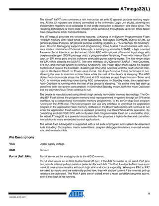
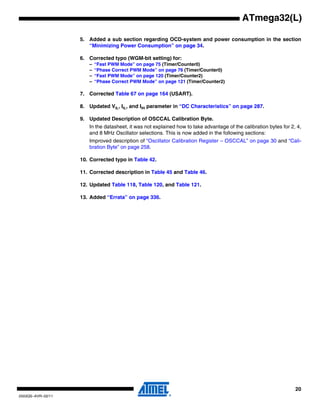
Register Summary
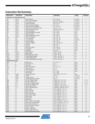
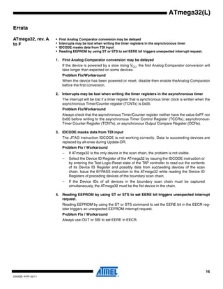
Address Name Bit 7 Bit 6 Bit 5 Bit 4 Bit 3 Bit 2 Bit 1 Bit 0 Page
$3F ($5F) SREG I T H S V N Z C 10
$3E ($5E) SPH – – – – SP11 SP10 SP9 SP8 12
$3D ($5D) SPL SP7 SP6 SP5 SP4 SP3 SP2 SP1 SP0 12
$3C ($5C) OCR0 Timer/Counter0 Output Compare Register 82
$3B ($5B) GICR INT1 INT0 INT2 – – – IVSEL IVCE 47, 67
$3A ($5A) GIFR INTF1 INTF0 INTF2 – – – – – 68
$39 ($59) TIMSK OCIE2 TOIE2 TICIE1 OCIE1A OCIE1B TOIE1 OCIE0 TOIE0 82, 112, 130
$38 ($58) TIFR OCF2 TOV2 ICF1 OCF1A OCF1B TOV1 OCF0 TOV0 83, 112, 130
$37 ($57) SPMCR SPMIE RWWSB – RWWSRE BLBSET PGWRT PGERS SPMEN 248
$36 ($56) TWCR TWINT TWEA TWSTA TWSTO TWWC TWEN – TWIE 177
$35 ($55) MCUCR SE SM2 SM1 SM0 ISC11 ISC10 ISC01 ISC00 32, 66
$34 ($54) MCUCSR JTD ISC2 – JTRF WDRF BORF EXTRF PORF 40, 67, 228
$33 ($53) TCCR0 FOC0 WGM00 COM01 COM00 WGM01 CS02 CS01 CS00 80
$32 ($52) TCNT0 Timer/Counter0 (8 Bits) 82
$31(1)
($51)(1)
OSCCAL Oscillator Calibration Register 30
OCDR On-Chip Debug Register 224
$30 ($50) SFIOR ADTS2 ADTS1 ADTS0 – ACME PUD PSR2 PSR10 56,85,131,198,218
$2F ($4F) TCCR1A COM1A1 COM1A0 COM1B1 COM1B0 FOC1A FOC1B WGM11 WGM10 107
$2E ($4E) TCCR1B ICNC1 ICES1 – WGM13 WGM12 CS12 CS11 CS10 110
$2D ($4D) TCNT1H Timer/Counter1 – Counter Register High Byte 111
$2C ($4C) TCNT1L Timer/Counter1 – Counter Register Low Byte 111
$2B ($4B) OCR1AH Timer/Counter1 – Output Compare Register A High Byte 111
$2A ($4A) OCR1AL Timer/Counter1 – Output Compare Register A Low Byte 111
$29 ($49) OCR1BH Timer/Counter1 – Output Compare Register B High Byte 111
$28 ($48) OCR1BL Timer/Counter1 – Output Compare Register B Low Byte 111
$27 ($47) ICR1H Timer/Counter1 – Input Capture Register High Byte 111
$26 ($46) ICR1L Timer/Counter1 – Input Capture Register Low Byte 111
$25 ($45) TCCR2 FOC2 WGM20 COM21 COM20 WGM21 CS22 CS21 CS20 125
$24 ($44) TCNT2 Timer/Counter2 (8 Bits) 127
$23 ($43) OCR2 Timer/Counter2 Output Compare Register 127
$22 ($42) ASSR – – – – AS2 TCN2UB OCR2UB TCR2UB 128
$21 ($41) WDTCR – – – WDTOE WDE WDP2 WDP1 WDP0 42
$20(2)
($40)(2)
UBRRH URSEL – – – UBRR[11:8] 164
UCSRC URSEL UMSEL UPM1 UPM0 USBS UCSZ1 UCSZ0 UCPOL 162
$1F ($3F) EEARH – – – – – – EEAR9 EEAR8 19
$1E ($3E) EEARL EEPROM Address Register Low Byte 19
$1D ($3D) EEDR EEPROM Data Register 19
$1C ($3C) EECR – – – – EERIE EEMWE EEWE EERE 19
$1B ($3B) PORTA PORTA7 PORTA6 PORTA5 PORTA4 PORTA3 PORTA2 PORTA1 PORTA0 64
$1A ($3A) DDRA DDA7 DDA6 DDA5 DDA4 DDA3 DDA2 DDA1 DDA0 64
$19 ($39) PINA PINA7 PINA6 PINA5 PINA4 PINA3 PINA2 PINA1 PINA0 64
$18 ($38) PORTB PORTB7 PORTB6 PORTB5 PORTB4 PORTB3 PORTB2 PORTB1 PORTB0 64
$17 ($37) DDRB DDB7 DDB6 DDB5 DDB4 DDB3 DDB2 DDB1 DDB0 64
$16 ($36) PINB PINB7 PINB6 PINB5 PINB4 PINB3 PINB2 PINB1 PINB0 65
$15 ($35) PORTC PORTC7 PORTC6 PORTC5 PORTC4 PORTC3 PORTC2 PORTC1 PORTC0 65
$14 ($34) DDRC DDC7 DDC6 DDC5 DDC4 DDC3 DDC2 DDC1 DDC0 65
$13 ($33) PINC PINC7 PINC6 PINC5 PINC4 PINC3 PINC2 PINC1 PINC0 65
$12 ($32) PORTD PORTD7 PORTD6 PORTD5 PORTD4 PORTD3 PORTD2 PORTD1 PORTD0 65
$11 ($31) DDRD DDD7 DDD6 DDD5 DDD4 DDD3 DDD2 DDD1 DDD0 65
$10 ($30) PIND PIND7 PIND6 PIND5 PIND4 PIND3 PIND2 PIND1 PIND0 65
$0F ($2F) SPDR SPI Data Register 138
$0E ($2E) SPSR SPIF WCOL – – – – – SPI2X 138
$0D ($2D) SPCR SPIE SPE DORD MSTR CPOL CPHA SPR1 SPR0 136
$0C ($2C) UDR USART I/O Data Register 159
$0B ($2B) UCSRA RXC TXC UDRE FE DOR PE U2X MPCM 160
$0A ($2A) UCSRB RXCIE TXCIE UDRIE RXEN TXEN UCSZ2 RXB8 TXB8 161
$09 ($29) UBRRL USART Baud Rate Register Low Byte 164
$08 ($28) ACSR ACD ACBG ACO ACI ACIE ACIC ACIS1 ACIS0 199
$07 ($27) ADMUX REFS1 REFS0 ADLAR MUX4 MUX3 MUX2 MUX1 MUX0 214
$06 ($26) ADCSRA ADEN ADSC ADATE ADIF ADIE ADPS2 ADPS1 ADPS0 216
$05 ($25) ADCH ADC Data Register High Byte 217
$04 ($24) ADCL ADC Data Register Low Byte 217
$03 ($23) TWDR Two-wire Serial Interface Data Register 179
$02 ($22) TWAR TWA6 TWA5 TWA4 TWA3 TWA2 TWA1 TWA0 TWGCE 179](https://image.slidesharecdn.com/a1-201121104837/85/Atmega-32-7-320.jpg)
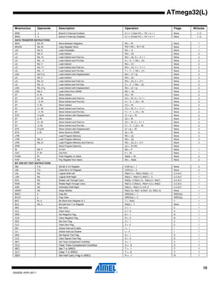
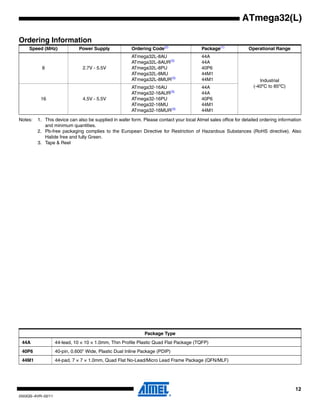
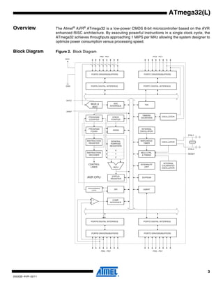
This document describes the features and specifications of the Atmel AVR ATmega32 8-bit microcontroller. It includes details about the microcontroller's architecture such as its instruction set, registers, memory, and peripherals. The document also provides information on the microcontroller's packaging, pinout, power consumption, and development tools support.


![[Deck] What's New in Spark-Iceberg Integration via DSV2.pptx](https://cdn.slidesharecdn.com/ss_thumbnails/deckwhatsnewinspark-icebergintegrationviadsv2-260210005337-25955b12-thumbnail.jpg?width=640&height=640&fit=bounds)


