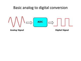
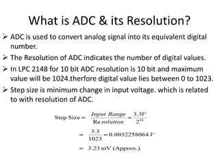
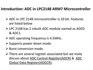
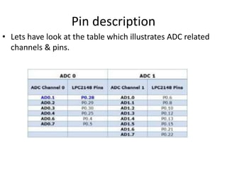
ADC
in LPC 2148 ARM Controller
LPC 2148 Microcontroller
LPC 2148 is very useful especially when it comes to
communicate with other devices
Basic analog to digital conversion
What is ADC & its Resolution?
 ADC is used to convert analog signal into its equivalent digital
number.
 The Resolution of ADC indicates the number of digital values.
 In LPC 2148 for 10 bit ADC resolution is 10 bit and maximum
value will be 1024.therfore digital value lies between 0 to 1023.
 Step size is minimum change in input voltage. which is related
to with resolution of ADC.
 ADC in LPC 2148 microcontroller is 10 bit. Features
are listed below
 LPC 2148 has 2 inbuilt ADC module named as ADC0
& ADC1.
 ADC operating frequency is 4.5MHz.
 Supports power down mode.
 Burst conversion mode.
 There are several register associated but we maily
discuss about ADC Control Register(ADCR) & ADC
Global Data Register(ADGCR).
Introduction: ADC in LPC2148 ARM7 Microcontroller
Pin description
• Lets have look at the table which illustrates ADC related
channels & pins.
Register description in ADC
• Register Name Function:-
• ADCRA/D Control Register: The ADCR register must be written to
select the operating mode before A/D conversion can occurs.
• ADGDRA/D Global Data Register: This register contains
ADC’s DONE bit and the result of the most recent A/D conversion.
• ADSTATA/D Status Register: This register contains DONE and
OVERRUN flag for all the A/D Channels, as well as the A/D interrupt
flag.
• ADGSRA/D Global Start Register: This address can be written (in
the AD0 address range) to start conversions in both A/D converters
simultaneously.
• ADINTENA/D Interrupt Enable Register: This register contains
enable bits that allow the DONE flag of each A/D channel to be
included or excluded from contributing to the generation of an A/D
interrupt.
• ADDRxA/D Channel x Data: ‘x’ varies from 0 to 7
analog to digital converter seminar

analog to digital converter seminar

  • 1.
    ADC in LPC 2148ARM Controller
  • 2.
    LPC 2148 Microcontroller LPC2148 is very useful especially when it comes to communicate with other devices
  • 3.
    Basic analog todigital conversion
  • 4.
    What is ADC& its Resolution?  ADC is used to convert analog signal into its equivalent digital number.  The Resolution of ADC indicates the number of digital values.  In LPC 2148 for 10 bit ADC resolution is 10 bit and maximum value will be 1024.therfore digital value lies between 0 to 1023.  Step size is minimum change in input voltage. which is related to with resolution of ADC.
  • 5.
     ADC inLPC 2148 microcontroller is 10 bit. Features are listed below  LPC 2148 has 2 inbuilt ADC module named as ADC0 & ADC1.  ADC operating frequency is 4.5MHz.  Supports power down mode.  Burst conversion mode.  There are several register associated but we maily discuss about ADC Control Register(ADCR) & ADC Global Data Register(ADGCR). Introduction: ADC in LPC2148 ARM7 Microcontroller
  • 6.
    Pin description • Letshave look at the table which illustrates ADC related channels & pins.
  • 7.
    Register description inADC • Register Name Function:- • ADCRA/D Control Register: The ADCR register must be written to select the operating mode before A/D conversion can occurs. • ADGDRA/D Global Data Register: This register contains ADC’s DONE bit and the result of the most recent A/D conversion. • ADSTATA/D Status Register: This register contains DONE and OVERRUN flag for all the A/D Channels, as well as the A/D interrupt flag. • ADGSRA/D Global Start Register: This address can be written (in the AD0 address range) to start conversions in both A/D converters simultaneously. • ADINTENA/D Interrupt Enable Register: This register contains enable bits that allow the DONE flag of each A/D channel to be included or excluded from contributing to the generation of an A/D interrupt. • ADDRxA/D Channel x Data: ‘x’ varies from 0 to 7