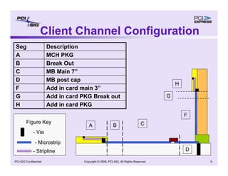
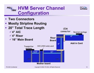
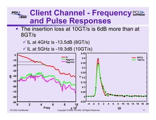
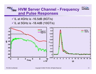
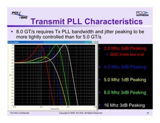
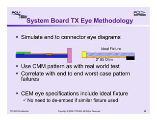
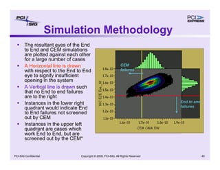
The document discusses requirements for the PCI Express 3.0 physical layer. It summarizes simulation results showing that 8 GT/s is feasible for target client and server channels with reasonable equalization, while 10 GT/s imposes a higher power penalty. It provides details on transmitter and receiver specifications, jitter budgets, and channel models used in simulations to evaluate maximum data rates. Key considerations for the PCIe 3.0 specification include transmitter parameters, receiver equalization techniques, and backwards compatibility.
![Copyright © 2008, PCI-SIG, All Rights Reserved 12
PCI-SIG Confidential
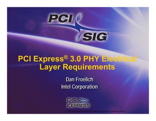
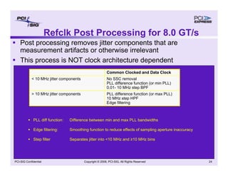
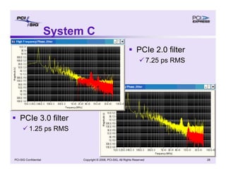
8GT/s
ps
Voltage
20 40 60 80 100 120
0.1
-0.05
0
-0.05
-0.1
-0.15 -12
-10
-8
-6
-4
-2
0
0.15
4 5 6 7 8
0
0.1
0.2
0.3
0.4
Time (nsec)
Amplitude
(V)
EQ pulse response
Un-EQ pulse response
ps
0.1
-0.05
0
-0.05
-0.1
-0.15 -12
-10
-8
-6
-4
-2
0
0.15
0
0.1
0.2
0.3
0.4
Amplitude
(V)
TX = [0.69 -0.31]
TX = [0.9 -0.1]
DFE =[0.1563 0.0781 0.0352 0 0.0156 0.0117]
Time (nsec)
10GT/s
EQ pulse response
Un-EQ pulse
response
4 5 6
20 40 60 80 100
TX = [1]
DFE =[1:6]
TX = [1]
EH = 16mV
EW = 10ps
EH = 27mV
EW = 11ps
Voltage
different equalization settings
Sample BER Eye Diagrams
1.0 UI
1.0 UI](https://image.slidesharecdn.com/03pcie3-231020160925-18bf76ef/85/03_PCIe_3-0_PHY_Electrical_Layer_Requirements_Final-1-pdf-12-320.jpg)
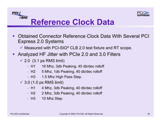
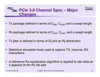
![Copyright © 2008, PCI-SIG, All Rights Reserved 14
PCI-SIG Confidential
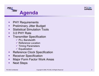
TX EQ
CTLE
DFE
Pass
Fail
[1]
1st
[1]
1st
[2 3]
[1]
[1 2]
[1]
[1-4 ]
[1]
[1-6 ]
Eye
Height
(V)
[1]
1st
8GT/s
10GT/s
-0.14
-0.12
-0.1
-0.08
-0.06
-0.04
-0.02
0
0.02
0.04
Equalization Sweep
20” Server Channel
Simulation Results (Nominal)
Power & Area
Power & Area
Pass
Fail
-0.1
-0.05
0
0.05
0.1
0.15
0.2
0.25
TX EQ
CTLE
DFE
[1]
1st
[1]
1st
[2 3]
[1]
[1 2]
[1]
[1-4 ]
[1]
[1-6 ]
[1]
1st
8GT/s
10GT/s
Eye
Height
(V)
7” Client Channel
Power & Area
Power & Area
TX EQ
CTLE
DFE
[1]
1st
[1]
1st
[2 3]
[1]
[1 2]
[1]
[1-4 ]
[1]
[1-6 ]
Eye
Height
(V)
Equalization Sweep
[1]
1st
-0.04
-0.02
0
0.02
0.04
0.06
0.08
8GT/s
10GT/s Pass
Fail
14” Client Channel
Power & Area
Power & Area](https://image.slidesharecdn.com/03pcie3-231020160925-18bf76ef/85/03_PCIe_3-0_PHY_Electrical_Layer_Requirements_Final-1-pdf-14-320.jpg)
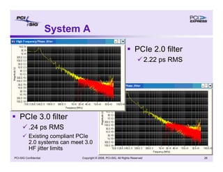
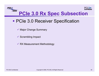
![Copyright © 2008, PCI-SIG, All Rights Reserved 15
PCI-SIG Confidential
Simulation Results (Est W/C)
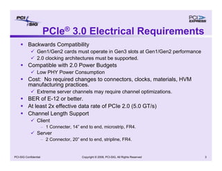
TX EQ
CTLE
DFE
[1]
1st
[1]
1st
[2 3]
[1]
[1 2]
[1]
[1-4 ]
[1]
[1-6 ]
Eye
Height
(V)
Equalization Sweep
[1]
1st
-0.04
-0.02
0
0.02
0.04
0.06
0.08
8GT/s
10GT/s
Pass
Fail
14” Client Channel
Power & Area
Power & Area
TX EQ
CTLE
DFE
Pass
Fail
[1]
1st
[1]
1st
[2 3]
[1]
[1 2]
[1]
[1-4 ]
[1]
[1-6 ]
Eye
Height
(V)
[1]
1st
8GT/s
10GT/s
-0.14
-0.12
-0.1
-0.08
-0.06
-0.04
-0.02
0
0.02
0.04
Equalization Sweep
20” Server Channel
Power & Area
Power & Area
Pass
Fail
-0.1
-0.05
0
0.05
0.1
0.15
0.2
0.25
TX EQ
CTLE
DFE
[1]
1st
[1]
1st
[2 3]
[1]
[1 2]
[1]
[1-4 ]
[1]
[1-6 ]
[1]
1st
8GT/s
10GT/s
Eye
Height
(V)
7” Client Channel
Power & Area
Power & Area](https://image.slidesharecdn.com/03pcie3-231020160925-18bf76ef/85/03_PCIe_3-0_PHY_Electrical_Layer_Requirements_Final-1-pdf-15-320.jpg)
![Signal Integrity - A Crash Course [R Lott]](https://cdn.slidesharecdn.com/ss_thumbnails/1cb0870c-cad3-4a68-ad41-8e9450fec5d8-170217191645-thumbnail.jpg?width=640&height=640&fit=bounds)


