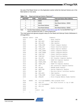
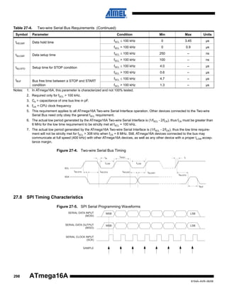
Downloaded 47 times

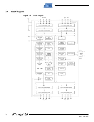
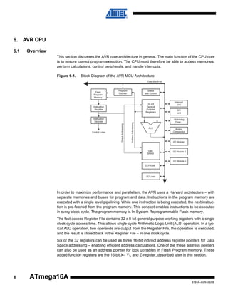
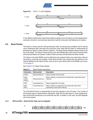
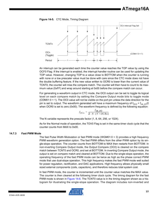
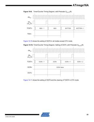
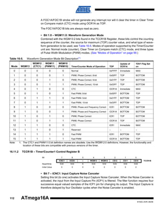
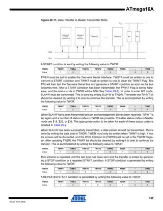
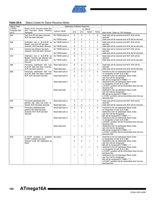
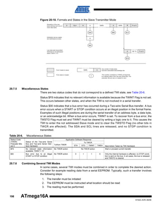
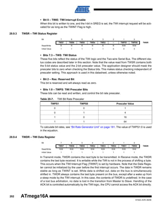
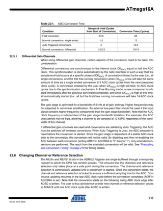
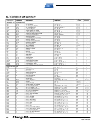
![Figure 10-1. Reset Logic
DATA BUS
PORF
BORF
EXTRF
WDRF
JTRF
MCU Control and Status
Register (MCUCSR)
Power-on
Reset Circuit
INTERNAL RESET
Brown-out
Reset Circuit
BODEN
BODLEVEL
Pull-up Resistor
Reset Circuit
JTAG Reset
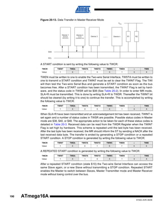
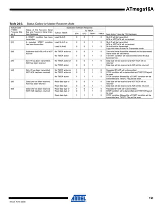
Register
Watchdog
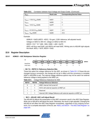
Timer
COUNTER RESET
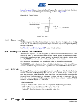
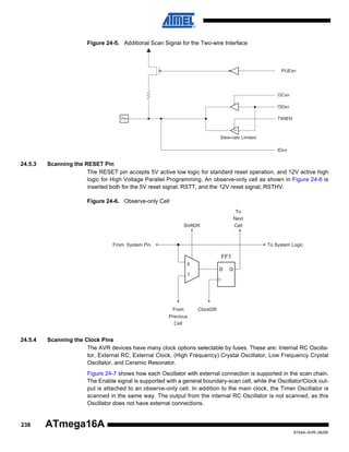
SPIKE
FILTER
Watchdog
Oscillator
Clock
Generator
CK
Delay Counters
TIMEOUT
CKSEL[3:0]
SUT[1:0]
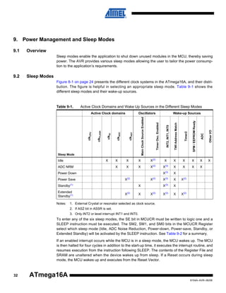
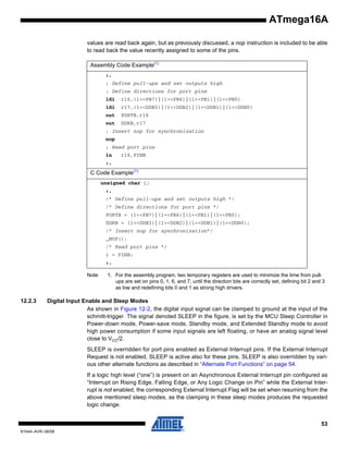
10.1.2
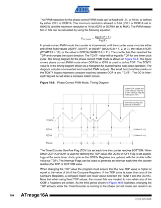
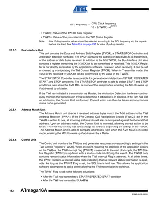
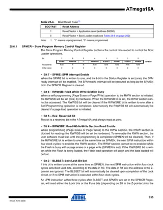
Power-on Reset
A Power-on Reset (POR) pulse is generated by an On-chip detection circuit. The detection level
is defined in “System and Reset Characteristics” on page 296. The POR is activated whenever
VCC is below the detection level. The POR circuit can be used to trigger the Start-up Reset, as
well as to detect a failure in supply voltage.
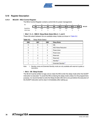
A Power-on Reset (POR) circuit ensures that the device is reset from Power-on. Reaching the
Power-on Reset threshold voltage invokes the delay counter, which determines how long the
device is kept in RESET after VCC rise. The RESET signal is activated again, without any delay,
when VCC decreases below the detection level.
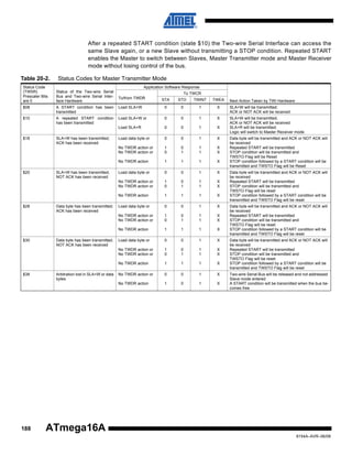
Figure 10-2. MCU Start-up, RESET Tied to VCC.
VCC
RESET
TIME-OUT
VPOT
VRST
tTOUT
INTERNAL
RESET
38
ATmega16A
8154A–AVR–06/08](https://image.slidesharecdn.com/atmega16a-140118085558-phpapp02/85/A-tmega16A-Microcontroller-Data-Sheet-38-320.jpg)
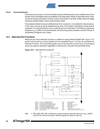
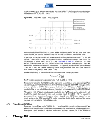
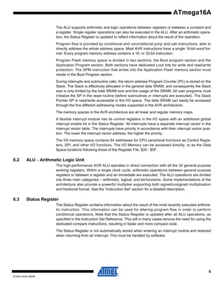
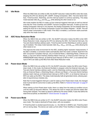
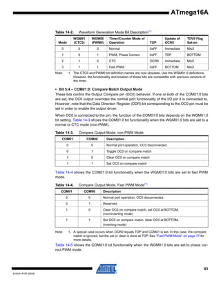
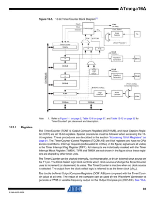
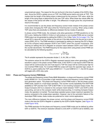
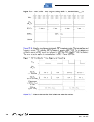
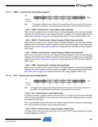
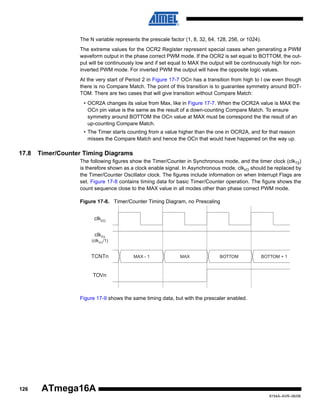
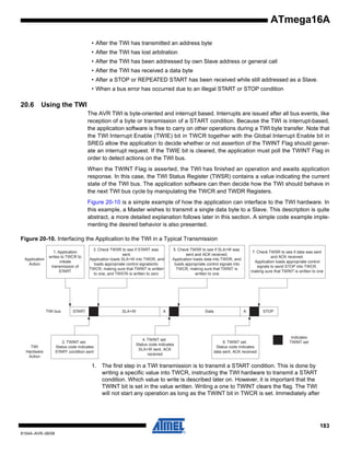
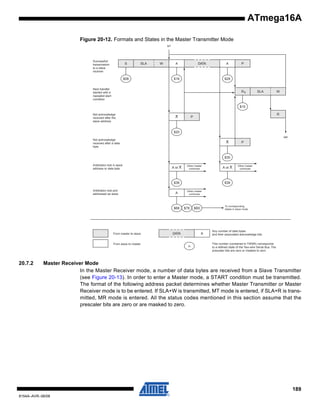
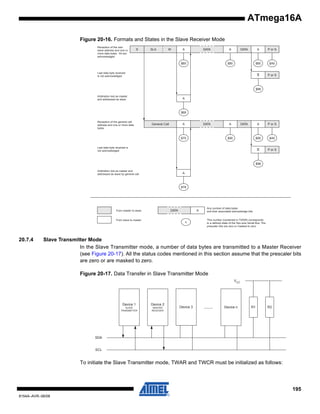
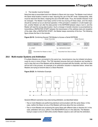
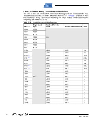
![Figure 14-11. Timer/Counter Timing Diagram, Clear Timer on Compare Match Mode, with Prescaler (fclk_I/O/8)
clkI/O
clkTn
(clkI/O /8)
TCNTn
(CTC)
TOP - 1
TOP
BOTTOM
OCRn
BOTTOM + 1
TOP
OCFn
14.9
14.9.1
Register Description
TCCR0 – Timer/Counter Control Register
Bit
7
6
5
4
3
2
1
0
FOC0
WGM00
COM01
COM00
WGM01
CS02
CS01
CS00
Read/Write
W
R/W
R/W
R/W
R/W
R/W
R/W
R/W
Initial Value
0
0
0
0
0
0
0
0
TCCR0
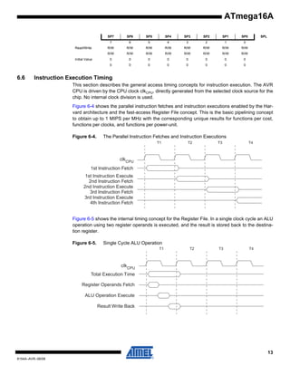
• Bit 7 – FOC0: Force Output Compare
The FOC0 bit is only active when the WGM00 bit specifies a non-PWM mode. However, for
ensuring compatibility with future devices, this bit must be set to zero when TCCR0 is written
when operating in PWM mode. When writing a logical one to the FOC0 bit, an immediate compare match is forced on the Waveform Generation unit. The OC0 output is changed according to
its COM01:0 bits setting. Note that the FOC0 bit is implemented as a strobe. Therefore it is the
value present in the COM01:0 bits that determines the effect of the forced compare.
A FOC0 strobe will not generate any interrupt, nor will it clear the timer in CTC mode using
OCR0 as TOP.
The FOC0 bit is always read as zero.
• Bit 3, 6 – WGM0[1:0]: Waveform Generation Mode
These bits control the counting sequence of the counter, the source for the maximum (TOP)
counter value, and what type of Waveform Generation to be used. Modes of operation supported by the Timer/Counter unit are: Normal mode, Clear Timer on Compare Match (CTC)
mode, and two types of Pulse Width Modulation (PWM) modes. See Table 14-2 and “Modes of
Operation” on page 76.
82
ATmega16A
8154A–AVR–06/08](https://image.slidesharecdn.com/atmega16a-140118085558-phpapp02/85/A-tmega16A-Microcontroller-Data-Sheet-82-320.jpg)
![Table 14-5.
Compare Output Mode, Phase Correct PWM Mode(1)
COM01
COM00
0
0
Normal port operation, OC0 disconnected.
0
1
Reserved
1
0
Clear OC0 on compare match when up-counting. Set OC0 on compare match
when downcounting.
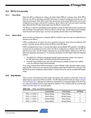
1
1
Set OC0 on compare match when up-counting. Clear OC0 on compare match
when downcounting.
Note:
Description
1. A special case occurs when OCR0 equals TOP and COM01 is set. In this case, the compare
match is ignored, but the set or clear is done at TOP. See “Phase Correct PWM Mode” on page
78 for more details.
• Bit 2:0 – CS02:0: Clock Select
The three Clock Select bits select the clock source to be used by the Timer/Counter.
Table 14-6.
Clock Select Bit Description
CS02
CS01
CS00
Description
0
0
0
No clock source (Timer/Counter stopped).
0
0
1
clkI/O/(No prescaling)
0
1
0
clkI/O/8 (From prescaler)
0
1
1
clkI/O/64 (From prescaler)
1
0
0
clkI/O/256 (From prescaler)
1
0
1
clkI/O/1024 (From prescaler)
1
1
0
External clock source on T0 pin. Clock on falling edge.
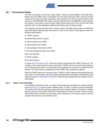
1
1
1
External clock source on T0 pin. Clock on rising edge.
If external pin modes are used for the Timer/Counter0, transitions on the T0 pin will clock the
counter even if the pin is configured as an output. This feature allows software control of the
counting.
14.9.2
TCNT0 – Timer/Counter Register
Bit
7
6
5
4
3
2
1
0
TCNT0[7:0]
TCNT0
Read/Write
R/W
R/W
R/W
R/W
R/W
R/W
R/W
R/W
Initial Value
0
0
0
0
0
0
0
0
The Timer/Counter Register gives direct access, both for read and write operations, to the
Timer/Counter unit 8-bit counter. Writing to the TCNT0 Register blocks (removes) the compare
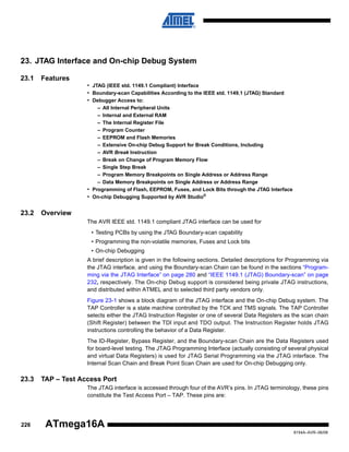
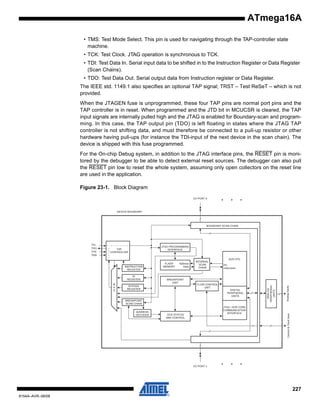
match on the following timer clock. Modifying the counter (TCNT0) while the counter is running,
introduces a risk of missing a compare match between TCNT0 and the OCR0 Register.
84
ATmega16A
8154A–AVR–06/08](https://image.slidesharecdn.com/atmega16a-140118085558-phpapp02/85/A-tmega16A-Microcontroller-Data-Sheet-84-320.jpg)
![ATmega16A
14.9.3
OCR0 – Output Compare Register
Bit
7
6
5
4
3
2
1
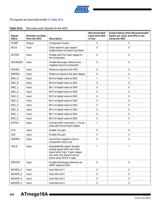
0
OCR0[7:0]
OCR0
Read/Write
R/W
R/W
R/W
R/W
R/W
R/W
R/W
R/W
Initial Value
0
0
0
0
0
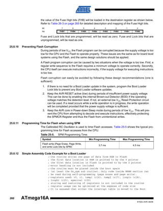
0
0
0
The Output Compare Register contains an 8-bit value that is continuously compared with the
counter value (TCNT0). A match can be used to generate an output compare interrupt, or to
generate a waveform output on the OC0 pin.
14.9.4
TIMSK – Timer/Counter Interrupt Mask Register
Bit
7
6
5
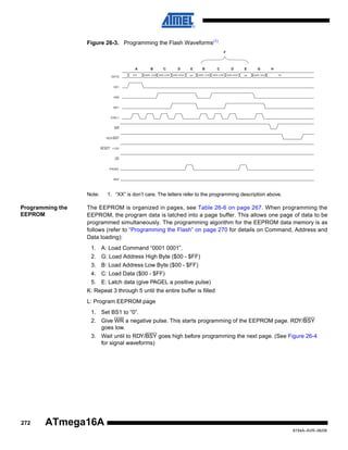
4
3
2
1
0
OCIE2
TOIE2
TICIE1
OCIE1A
OCIE1B
TOIE1
OCIE0
TOIE0
Read/Write
R/W
R/W
R/W
R/W
R/W
R/W
R/W
R/W
Initial Value
0
0
0
0
0
0
0
0
TIMSK
• Bit 1 – OCIE0: Timer/Counter0 Output Compare Match Interrupt Enable
When the OCIE0 bit is written to one, and the I-bit in the Status Register is set (one), the
Timer/Counter0 Compare Match interrupt is enabled. The corresponding interrupt is executed if
a compare match in Timer/Counter0 occurs, i.e., when the OCF0 bit is set in the Timer/Counter
Interrupt Flag Register – TIFR.
• Bit 0 – TOIE0: Timer/Counter0 Overflow Interrupt Enable
When the TOIE0 bit is written to one, and the I-bit in the Status Register is set (one), the
Timer/Counter0 Overflow interrupt is enabled. The corresponding interrupt is executed if an
overflow in Timer/Counter0 occurs, i.e., when the TOV0 bit is set in the Timer/Counter Interrupt
Flag Register – TIFR.
14.9.5
TIFR qP Timer/Counter Interrupt Flag Register
Bit
7
6
5
4
3
2
1
0
OCF2
TOV2
ICF1
OCF1A
OCF1B
TOV1
OCF0
TOV0
Read/Write
R/W
R/W
R/W
R/W
R/W
R/W
R/W
R/W
Initial Value
0
0
0
0
0
0
0
0
TIFR
• Bit 1 – OCF0: Output Compare Flag 0
The OCF0 bit is set (one) when a compare match occurs between the Timer/Counter0 and the
data in OCR0 – Output Compare Register0. OCF0 is cleared by hardware when executing the
corresponding interrupt handling vector. Alternatively, OCF0 is cleared by writing a logic one to
the flag. When the I-bit in SREG, OCIE0 (Timer/Counter0 Compare Match Interrupt Enable), and
OCF0 are set (one), the Timer/Counter0 Compare Match Interrupt is executed.
• Bit 0 – TOV0: Timer/Counter0 Overflow Flag
The bit TOV0 is set (one) when an overflow occurs in Timer/Counter0. TOV0 is cleared by hardware when executing the corresponding interrupt handling vector. Alternatively, TOV0 is cleared
by writing a logic one to the flag. When the SREG I-bit, TOIE0 (Timer/Counter0 Overflow Interrupt Enable), and TOV0 are set (one), the Timer/Counter0 Overflow interrupt is executed. In
phase correct PWM mode, this bit is set when Timer/Counter0 changes counting direction at
$00.
85
8154A–AVR–06/08](https://image.slidesharecdn.com/atmega16a-140118085558-phpapp02/85/A-tmega16A-Microcontroller-Data-Sheet-85-320.jpg)
![ATmega16A
• Bit 6 – ICES1: Input Capture Edge Select
This bit selects which edge on the Input Capture Pin (ICP1) that is used to trigger a capture
event. When the ICES1 bit is written to zero, a falling (negative) edge is used as trigger, and
when the ICES1 bit is written to one, a rising (positive) edge will trigger the capture.
When a capture is triggered according to the ICES1 setting, the counter value is copied into the
Input Capture Register (ICR1). The event will also set the Input Capture Flag (ICF1), and this
can be used to cause an Input Capture Interrupt, if this interrupt is enabled.
When the ICR1 is used as TOP value (see description of the WGM13:0 bits located in the
TCCR1A and the TCCR1B Register), the ICP1 is disconnected and consequently the Input Capture function is disabled.
• Bit 5 – Reserved Bit
This bit is reserved for future use. For ensuring compatibility with future devices, this bit must be
written to zero when TCCR1B is written.
• Bit 4:3 – WGM13:2: Waveform Generation Mode
See TCCR1A Register description.
• Bit 2:0 – CS12:0: Clock Select
The three Clock Select bits select the clock source to be used by the Timer/Counter, see Figure
16-10 and Figure 16-11.
Table 16-6.
CS12
Clock Select Bit Description
CS11
CS10
Description
0
0
0
No clock source (Timer/Counter stopped).
0
0
1
clkI/O/1 (No prescaling)
0
1
0
clkI/O/8 (From prescaler)
0
1
1
clkI/O/64 (From prescaler)
1
0
0
clkI/O/256 (From prescaler)
1
0
1
clkI/O/1024 (From prescaler)
1
1
0
External clock source on T1 pin. Clock on falling edge.
1
1
1
External clock source on T1 pin. Clock on rising edge.
If external pin modes are used for the Timer/Counter1, transitions on the T1 pin will clock the
counter even if the pin is configured as an output. This feature allows software control of the
counting.
16.11.3
TCNT1H and TCNT1L –Timer/Counter1 High and Low Register
Bit
7
6
5
4
3
2
1
0
TCNT1[15:8]
TCNT1H
TCNT1[7:0]
TCNT1L
Read/Write
R/W
R/W
R/W
R/W
R/W
R/W
R/W
R/W
Initial Value
0
0
0
0
0
0
0
0
The two Timer/Counter I/O locations (TCNT1H and TCNT1L, combined TCNT1) give direct
access, both for read and for write operations, to the Timer/Counter unit 16-bit counter. To
113
8154A–AVR–06/08](https://image.slidesharecdn.com/atmega16a-140118085558-phpapp02/85/A-tmega16A-Microcontroller-Data-Sheet-113-320.jpg)
![ensure that both the high and Low bytes are read and written simultaneously when the CPU
accesses these registers, the access is performed using an 8-bit temporary High Byte Register
(TEMP). This temporary register is shared by all the other 16-bit registers. See “Accessing 16-bit
Registers” on page 91.
Modifying the counter (TCNT1) while the counter is running introduces a risk of missing a compare match between TCNT1 and one of the OCR1x Registers.
Writing to the TCNT1 Register blocks (removes) the compare match on the following timer clock
for all compare units.
16.11.4
OCR1AH and OCR1AL – Output Compare Register 1 A
Bit
7
6
5
4
3
2
1
0
OCR1A[15:8]
OCR1AH
OCR1A[7:0]
OCR1AL
Read/Write
R/W
R/W
R/W
R/W
R/W
R/W
R/W
Initial Value
16.11.5
R/W
0
0
0
0
0
0
0
0
4
3
2
1
0
OCR1BH and OCR1BL – Output Compare Register 1 B
Bit
7
6
5
OCR1B[15:8]
OCR1BH
OCR1B[7:0]
OCR1BL
Read/Write
R/W
R/W
R/W
R/W
R/W
R/W
R/W
R/W
Initial Value
0
0
0
0
0
0
0
0
The Output Compare Registers contain a 16-bit value that is continuously compared with the
counter value (TCNT1). A match can be used to generate an output compare interrupt, or to
generate a waveform output on the OC1x pin.
The Output Compare Registers are 16-bit in size. To ensure that both the high and Low bytes
are written simultaneously when the CPU writes to these registers, the access is performed
using an 8-bit temporary High Byte Register (TEMP). This temporary register is shared by all the
other 16-bit registers. See “Accessing 16-bit Registers” on page 91.
16.11.6
ICR1H and ICR1L – Input Capture Register 1
Bit
7
6
5
4
3
2
1
0
ICR1[15:8]
ICR1H
ICR1[7:0]
ICR1L
Read/Write
R/W
R/W
R/W
R/W
R/W
R/W
R/W
R/W
Initial Value
0
0
0
0
0
0
0
0
The Input Capture is updated with the counter (TCNT1) value each time an event occurs on the
ICP1 pin (or optionally on the analog comparator output for Timer/Counter1). The Input Capture
can be used for defining the counter TOP value.
The Input Capture Register is 16-bit in size. To ensure that both the high and Low bytes are read
simultaneously when the CPU accesses these registers, the access is performed using an 8-bit
temporary High Byte Register (TEMP). This temporary register is shared by all the other 16-bit
registers. See “Accessing 16-bit Registers” on page 91.
114
ATmega16A
8154A–AVR–06/08](https://image.slidesharecdn.com/atmega16a-140118085558-phpapp02/85/A-tmega16A-Microcontroller-Data-Sheet-114-320.jpg)

![ATmega16A
A FOC2 strobe will not generate any interrupt, nor will it clear the timer in CTC mode using
OCR2 as TOP.
The FOC2 bit is always read as zero.
• Bit 3, 6 – WGM2[1:0]: Waveform Generation Mode
These bits control the counting sequence of the counter, the source for the maximum (TOP)
counter value, and what type of waveform generation to be used. Modes of operation supported
by the Timer/Counter unit are: Normal mode, Clear Timer on Compare match (CTC) mode, and
two types of Pulse Width Modulation (PWM) modes. See Table 17-2 and “Modes of Operation”
on page 122.
Table 17-2.
Waveform Generation Mode Bit Description(1)
Mode
WGM21
(CTC2)
WGM20
(PWM2)
Timer/Counter Mode of
Operation
TOP
Update of
OCR2
TOV2 Flag
Set on
0
0
0
Normal
0xFF
Immediate
MAX
1
0
1
PWM, Phase Correct
0xFF
TOP
BOTTOM
2
1
0
CTC
OCR2
Immediate
MAX
3
1
1
Fast PWM
0xFF
BOTTOM
MAX
Note:
1. The CTC2 and PWM2 bit definition names are now obsolete. Use the WGM21:0 definitions.
However, the functionality and location of these bits are compatible with previous versions of
the timer.
• Bit 5:4 – COM21:0: Compare Match Output Mode
These bits control the Output Compare pin (OC2) behavior. If one or both of the COM21:0 bits
are set, the OC2 output overrides the normal port functionality of the I/O pin it is connected to.
However, note that the Data Direction Register (DDR) bit corresponding to OC2 pin must be set
in order to enable the output driver.
When OC2 is connected to the pin, the function of the COM21:0 bits depends on the WGM21:0
bit setting. Table 17-3 shows the COM21:0 bit functionality when the WGM21:0 bits are set to a
normal or CTC mode (non-PWM).
Table 17-3.
Compare Output Mode, non-PWM Mode
COM21
COM20
Description
0
0
Normal port operation, OC2 disconnected.
0
1
Toggle OC2 on compare match
1
0
Clear OC2 on compare match
1
1
Set OC2 on compare match
131
8154A–AVR–06/08](https://image.slidesharecdn.com/atmega16a-140118085558-phpapp02/85/A-tmega16A-Microcontroller-Data-Sheet-131-320.jpg)
![ATmega16A
17.11.2
TCNT2 – Timer/Counter Register
Bit
7
6
5
4
3
2
1
0
TCNT2[7:0]
TCNT2
Read/Write
R/W
R/W
R/W
R/W
R/W
R/W
R/W
R/W
Initial Value
0
0
0
0
0
0
0
0
The Timer/Counter Register gives direct access, both for read and write operations, to the
Timer/Counter unit 8-bit counter. Writing to the TCNT2 Register blocks (removes) the compare
match on the following timer clock. Modifying the counter (TCNT2) while the counter is running,
introduces a risk of missing a compare match between TCNT2 and the OCR2 Register.
17.11.3
OCR2 – Output Compare Register
Bit
7
6
5
4
3
2
1
0
OCR2[7:0]
OCR2
Read/Write
R/W
R/W
R/W
R/W
R/W
R/W
R/W
R/W
Initial Value
0
0
0
0
0
0
0
0
The Output Compare Register contains an 8-bit value that is continuously compared with the
counter value (TCNT2). A match can be used to generate an output compare interrupt, or to
generate a waveform output on the OC2 pin.
17.11.4
ASSR – Asynchronous Status Register
Bit
7
6
5
4
3
2
1
0
–
–
–
–
AS2
TCN2UB
OCR2UB
TCR2UB
Read/Write
R
R
R
R
R/W
R
R
R
Initial Value
0
0
0
0
0
0
0
0
ASSR
• Bit 3 – AS2: Asynchronous Timer/Counter2
When AS2 is written to zero, Timer/Counter 2 is clocked from the I/O clock, clkI/O. When AS2 is
written to one, Timer/Counter2 is clocked from a Crystal Oscillator connected to the Timer Oscillator 1 (TOSC1) pin. When the value of AS2 is changed, the contents of TCNT2, OCR2, and
TCCR2 might be corrupted.
• Bit 2 – TCN2UB: Timer/Counter2 Update Busy
When Timer/Counter2 operates asynchronously and TCNT2 is written, this bit becomes set.
When TCNT2 has been updated from the temporary storage register, this bit is cleared by hardware. A logical zero in this bit indicates that TCNT2 is ready to be updated with a new value.
• Bit 1 – OCR2UB: Output Compare Register2 Update Busy
When Timer/Counter2 operates asynchronously and OCR2 is written, this bit becomes set.
When OCR2 has been updated from the temporary storage register, this bit is cleared by hardware. A logical zero in this bit indicates that OCR2 is ready to be updated with a new value.
• Bit 0 – TCR2UB: Timer/Counter Control Register2 Update Busy
When Timer/Counter2 operates asynchronously and TCCR2 is written, this bit becomes set.
When TCCR2 has been updated from the temporary storage register, this bit is cleared by hardware. A logical zero in this bit indicates that TCCR2 is ready to be updated with a new value.
If a write is performed to any of the three Timer/Counter2 Registers while its update busy flag is
set, the updated value might get corrupted and cause an unintentional interrupt to occur.
133
8154A–AVR–06/08](https://image.slidesharecdn.com/atmega16a-140118085558-phpapp02/85/A-tmega16A-Microcontroller-Data-Sheet-133-320.jpg)
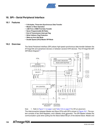
![ATmega16A
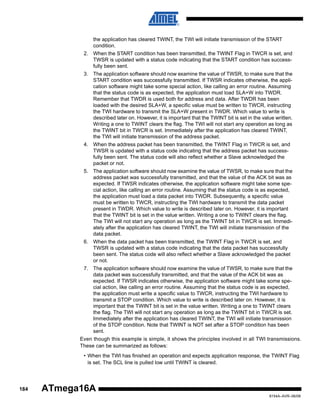
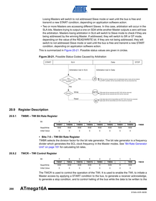
Figure 19-1. USART Block Diagram(1)
Clock Generator
UBRR[H:L]
OSC
BAUD RATE GENERATOR
SYNC LOGIC
PIN
CONTROL
XCK
Transmitter
TX
CONTROL
UDR (Transmit)
DATABUS
PARITY
GENERATOR
PIN
CONTROL
TRANSMIT SHIFT REGISTER
Receiver
CLOCK
RECOVERY
DATA
RECOVERY
PIN
CONTROL
UDR (Receive)
UCSRA
RX
CONTROL
RECEIVE SHIFT REGISTER
Note:
TxD
PARITY
CHECKER
UCSRB
RxD
UCSRC
1. Refer to Figure 1-1 on page 2, Table 12-14 on page 64, and Table 12-8 on page 59 for USART
pin placement.
The dashed boxes in the block diagram separate the three main parts of the USART (listed from
the top): Clock Generator, Transmitter and Receiver. Control Registers are shared by all units.
The clock generation logic consists of synchronization logic for external clock input used by synchronous Slave operation, and the baud rate generator. The XCK (Transfer Clock) pin is only
used by Synchronous Transfer mode. The Transmitter consists of a single write buffer, a serial
Shift Register, parity generator and control logic for handling different serial frame formats. The
write buffer allows a continuous transfer of data without any delay between frames. The
Receiver is the most complex part of the USART module due to its clock and data recovery
units. The recovery units are used for asynchronous data reception. In addition to the recovery
units, the receiver includes a parity checker, control logic, a Shift Register and a two level
receive buffer (UDR). The receiver supports the same frame formats as the transmitter, and can
detect frame error, data overrun and parity errors.
147
8154A–AVR–06/08](https://image.slidesharecdn.com/atmega16a-140118085558-phpapp02/85/A-tmega16A-Microcontroller-Data-Sheet-147-320.jpg)
![ATmega16A
Figure 19-3. Synchronous Mode XCK Timing.
UCPOL = 1
XCK
RxD / TxD
Sample
UCPOL = 0
XCK
RxD / TxD
Sample
The UCPOL bit UCRSC selects which XCK clock edge is used for data sampling and which is
used for data change. As Figure 19-3 shows, when UCPOL is zero the data will be changed at
rising XCK edge and sampled at falling XCK edge. If UCPOL is set, the data will be changed at
falling XCK edge and sampled at rising XCK edge.
19.4
Frame Formats
A serial frame is defined to be one character of data bits with synchronization bits (start and stop
bits), and optionally a parity bit for error checking. The USART accepts all 30 combinations of
the following as valid frame formats:
• 1 start bit
• 5, 6, 7, 8, or 9 data bits
• no, even or odd parity bit
• 1 or 2 stop bits
A frame starts with the start bit followed by the least significant data bit. Then the next data bits,
up to a total of nine, are succeeding, ending with the most significant bit. If enabled, the parity bit
is inserted after the data bits, before the stop bits. When a complete frame is transmitted, it can
be directly followed by a new frame, or the communication line can be set to an idle (high) state.
Figure 19-4 illustrates the possible combinations of the frame formats. Bits inside brackets are
optional.
Figure 19-4. Frame Formats
FRAME
(IDLE)
St
0
1
2
3
4
[5]
[6]
[7]
[8]
[P] Sp1 [Sp2]
(St / IDLE)
St
Start bit, always low.
(n)
Data bits (0 to 8).
P
Parity bit. Can be odd or even.
Sp
Stop bit, always high.
IDLE
No transfers on the communication line (RxD or TxD). An IDLE line must
be
high.
151
8154A–AVR–06/08](https://image.slidesharecdn.com/atmega16a-140118085558-phpapp02/85/A-tmega16A-Microcontroller-Data-Sheet-151-320.jpg)
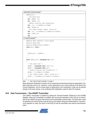
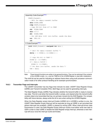
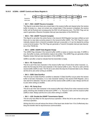
![USART_ReadUCSRC:
; Read UCSRC
in r16,UBRRH
in r16,UCSRC
ret
C Code Example(1)
unsigned char USART_ReadUCSRC( void )
{
unsigned char ucsrc;
/* Read UCSRC */
ucsrc = UBRRH;
ucsrc = UCSRC;
return ucsrc;
}
Note:
1. See “About Code Examples” on page 7.
The assembly code example returns the UCSRC value in r16.
Reading the UBRRH contents is not an atomic operation and therefore it can be read as an ordinary register, as long as the previous instruction did not access the register location.
19.10.3
Register Description
19.10.4
UDR – USART I/O Data Register
Bit
7
6
5
4
3
2
1
0
RXB[7:0]
UDR (Read)
TXB[7:0]
UDR (Write)
Read/Write
R/W
R/W
R/W
R/W
R/W
R/W
R/W
R/W
Initial Value
0
0
0
0
0
0
0
0
The USART Transmit Data Buffer Register and USART Receive Data Buffer Registers share the
same I/O address referred to as USART Data Register or UDR. The Transmit Data Buffer Register (TXB) will be the destination for data written to the UDR Register location. Reading the
UDR Register location will return the contents of the Receive Data Buffer Register (RXB).
For 5-, 6-, or 7-bit characters the upper unused bits will be ignored by the Transmitter and set to
zero by the Receiver.
The transmit buffer can only be written when the UDRE Flag in the UCSRA Register is set. Data
written to UDR when the UDRE Flag is not set, will be ignored by the USART Transmitter. When
data is written to the transmit buffer, and the Transmitter is enabled, the Transmitter will load the
data into the transmit Shift Register when the Shift Register is empty. Then the data will be serially transmitted on the TxD pin.
The receive buffer consists of a two level FIFO. The FIFO will change its state whenever the
receive buffer is accessed. Due to this behavior of the receive buffer, do not use read modify
write instructions (SBI and CBI) on this location. Be careful when using bit test instructions (SBIC
and SBIS), since these also will change the state of the FIFO.
166
ATmega16A
8154A–AVR–06/08](https://image.slidesharecdn.com/atmega16a-140118085558-phpapp02/85/A-tmega16A-Microcontroller-Data-Sheet-166-320.jpg)
![• Bit 2:1 – UCSZ1:0: Character Size
The UCSZ1:0 bits combined with the UCSZ2 bit in UCSRB sets the number of data bits (Character Size) in a frame the Receiver and Transmitter use.
Table 19-7.
UCSZ Bits Settings
UCSZ2
UCSZ1
UCSZ0
Character Size
0
0
0
5-bit
0
0
1
6-bit
0
1
0
7-bit
0
1
1
8-bit
1
0
0
Reserved
1
0
1
Reserved
1
1
0
Reserved
1
1
1
9-bit
• Bit 0 – UCPOL: Clock Polarity
This bit is used for Synchronous mode only. Write this bit to zero when Asynchronous mode is
used. The UCPOL bit sets the relationship between data output change and data input sample,
and the synchronous clock (XCK).
Table 19-8.
UCPOL Bit Settings
Transmitted Data Changed (Output of TxD
Pin)
Received Data Sampled (Input on RxD
Pin)
0
Rising XCK Edge
Falling XCK Edge
1
Falling XCK Edge
Rising XCK Edge
UCPOL
19.10.8
UBRRL and UBRRH – USART Baud Rate Registers
Bit
15
14
13
12
URSEL
–
–
–
11
10
9
8
UBRR[11:8]
UBRRH
UBRR[7:0]
7
Read/Write
6
5
UBRRL
4
3
2
1
0
R
R
R
R/W
R/W
R/W
R/W
R/W
R/W
R/W
R/W
R/W
R/W
R/W
R/W
0
0
0
0
0
0
0
0
0
Initial Value
R/W
0
0
0
0
0
0
0
The UBRRH Register shares the same I/O location as the UCSRC Register. See the “Accessing
UBRRH/ UCSRC Registers” on page 164 section which describes how to access this register.
• Bit 15 – URSEL: Register Select
This bit selects between accessing the UBRRH or the UCSRC Register. It is read as zero when
reading UBRRH. The URSEL must be zero when writing the UBRRH.
• Bit 14:12 – Reserved Bits
These bits are reserved for future use. For compatibility with future devices, these bit must be
written to zero when UBRRH is written.
170
ATmega16A
8154A–AVR–06/08](https://image.slidesharecdn.com/atmega16a-140118085558-phpapp02/85/A-tmega16A-Microcontroller-Data-Sheet-170-320.jpg)
![ATmega16A
• Bit 11:0 – UBRR11:0: USART Baud Rate Register
This is a 12-bit register which contains the USART baud rate. The UBRRH contains the four
most significant bits, and the UBRRL contains the 8 least significant bits of the USART baud
rate. Ongoing transmissions by the transmitter and receiver will be corrupted if the baud rate is
changed. Writing UBRRL will trigger an immediate update of the baud rate prescaler.
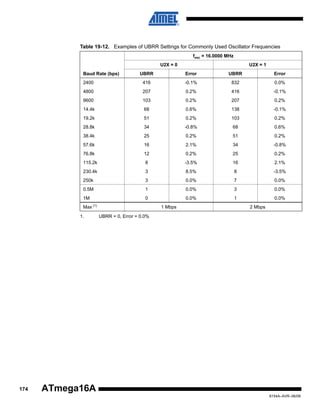
19.11 Examples of Baud Rate Setting
For standard crystal and resonator frequencies, the most commonly used baud rates for asynchronous operation can be generated by using the UBRR settings in Table 19-9. UBRR values
which yield an actual baud rate differing less than 0.5% from the target baud rate, are bold in the
table. Higher error ratings are acceptable, but the receiver will have less noise resistance when
the error ratings are high, especially for large serial frames (see “Asynchronous Operational
Range” on page 162). The error values are calculated using the following equation:
BaudRate Closest Match
Error[%] = ⎛ ------------------------------------------------------- – 1⎞ • 100%
⎝
⎠
BaudRate
Table 19-9.
Examples of UBRR Settings for Commonly Used Oscillator Frequencies
fosc = 1.0000 MHz
fosc = 1.8432 MHz
fosc = 2.0000 MHz
Baud
Rate
(bps)
UBRR
Error
UBRR
Error
UBRR
Error
UBRR
Error
UBRR
Error
UBRR
Error
2400
25
0.2%
51
0.2%
47
0.0%
95
0.0%
51
0.2%
103
0.2%
4800
12
0.2%
25
0.2%
23
0.0%
47
0.0%
25
0.2%
51
0.2%
9600
6
-7.0%
12
0.2%
11
0.0%
23
0.0%
12
0.2%
25
0.2%
14.4k
3
8.5%
8
-3.5%
7
0.0%
15
0.0%
8
-3.5%
16
2.1%
19.2k
2
8.5%
6
-7.0%
5
0.0%
11
0.0%
6
-7.0%
12
0.2%
28.8k
1
8.5%
3
8.5%
3
0.0%
7
0.0%
3
8.5%
8
-3.5%
38.4k
1
-18.6%
2
8.5%
2
0.0%
5
0.0%
2
8.5%
6
-7.0%
57.6k
0
8.5%
1
8.5%
1
0.0%
3
0.0%
1
8.5%
3
8.5%
76.8k
–
–
1
-18.6%
1
-25.0%
2
0.0%
1
-18.6%
2
8.5%
115.2k
–
–
0
8.5%
0
0.0%
1
0.0%
0
8.5%
1
8.5%
230.4k
–
–
–
–
–
–
0
0.0%
–
–
–
–
250k
–
–
–
–
–
–
–
–
–
–
0
0.0%
Max
1.
U2X = 0
(1)
U2X = 1
62.5 kbps
125 kbps
U2X = 0
U2X = 1
115.2 kbps
U2X = 0
230.4 kbps
125 kbps
U2X = 1
250 kbps
UBRR = 0, Error = 0.0%
171
8154A–AVR–06/08](https://image.slidesharecdn.com/atmega16a-140118085558-phpapp02/85/A-tmega16A-Microcontroller-Data-Sheet-171-320.jpg)
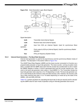
![ATmega16A
• Bits 7:0 – TWD: TWI Data Register
These eight bits contain the next data byte to be transmitted, or the latest data byte received on
the Two-wire Serial Bus.
20.9.5
TWA R– TWI (Slave) Address Register
Bit
7
6
5
4
3
2
1
0
TWA6
TWA5
TWA4
TWA3
TWA2
TWA1
TWA0
TWGCE
Read/Write
R/W
R/W
R/W
R/W
R/W
R/W
R/W
R/W
Initial Value
1
1
1
1
1
1
1
0
TWAR
The TWAR should be loaded with the 7-bit Slave address (in the seven most significant bits of
TWAR) to which the TWI will respond when programmed as a Slave Transmitter or receiver. In
multi-master systems, TWAR must be set in Masters which can be addressed as Slaves by
other Masters.
The LSB of TWAR is used to enable recognition of the general call address ($00). There is an
associated address comparator that looks for the Slave address (or general call address if
enabled) in the received serial address. If a match is found, an interrupt request is generated.
• Bits 7:1 – TWA[6:0]: TWI (Slave) Address Register
These seven bits constitute the Slave address of the TWI unit.
• Bit 0 – TWGCE: TWI General Call Recognition Enable Bit
If set, this bit enables the recognition of a General Call given over the Two-wire Serial Bus.
203
8154A–AVR–06/08](https://image.slidesharecdn.com/atmega16a-140118085558-phpapp02/85/A-tmega16A-Microcontroller-Data-Sheet-203-320.jpg)
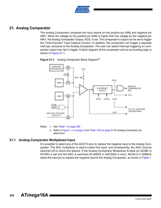
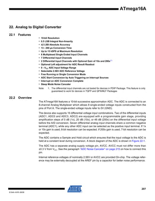
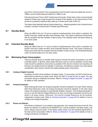
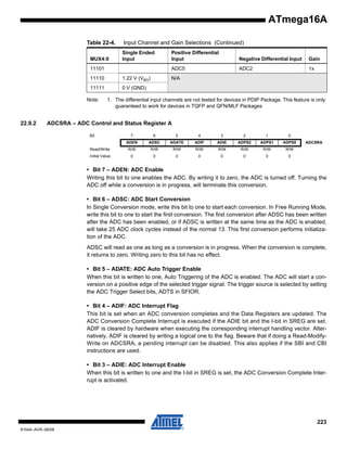
![Figure 22-1. Analog to Digital Converter Block Schematic
ADC CONVERSION
COMPLETE IRQ
INTERRUPT
FLAGS
ADTS[2:0]
TRIGGER
SELECT
ADC[9:0]
ADPS1
0
ADC DATA REGISTER
(ADCH/ADCL)
ADPS0
ADPS2
ADIF
ADATE
ADEN
ADSC
MUX1
15
ADC CTRL. & STATUS
REGISTER (ADCSRA)
MUX0
MUX3
MUX2
MUX4
ADLAR
REFS0
REFS1
ADC MULTIPLEXER
SELECT (ADMUX)
ADIE
ADIF
8-BIT DATA BUS
AVCC
PRESCALER
START
GAIN SELECTION
CHANNEL SELECTION
MUX DECODER
CONVERSION LOGIC
INTERNAL 2.56V
REFERENCE
SAMPLE & HOLD
COMPARATOR
AREF
10-BIT DAC
+
GND
BANDGAP
REFERENCE
ADC7
SINGLE ENDED / DIFFERENTIAL SELECTION
ADC6
ADC5
ADC MULTIPLEXER
OUTPUT
POS.
INPUT
MUX
ADC4
ADC3
+
ADC2
GAIN
AMPLIFIER
ADC1
ADC0
NEG.
INPUT
MUX
22.3
Operation
The ADC converts an analog input voltage to a 10-bit digital value through successive approximation. The minimum value represents GND and the maximum value represents the voltage on
the AREF pin minus 1 LSB. Optionally, AVCC or an internal 2.56V reference voltage may be
connected to the AREF pin by writing to the REFSn bits in the ADMUX Register. The internal
voltage reference may thus be decoupled by an external capacitor at the AREF pin to improve
noise immunity.
The analog input channel and differential gain are selected by writing to the MUX bits in
ADMUX. Any of the ADC input pins, as well as GND and a fixed bandgap voltage reference, can
be selected as single ended inputs to the ADC. A selection of ADC input pins can be selected as
positive and negative inputs to the differential gain amplifier.
208
ATmega16A
8154A–AVR–06/08](https://image.slidesharecdn.com/atmega16a-140118085558-phpapp02/85/A-tmega16A-Microcontroller-Data-Sheet-208-320.jpg)
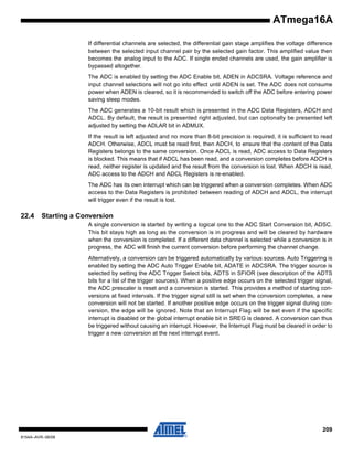
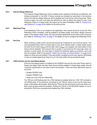
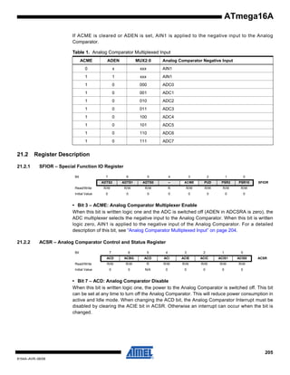
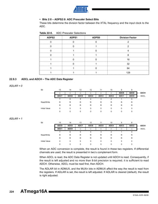
![Figure 22-2. ADC Auto Trigger Logic
ADTS[2:0]
PRESCALER
START
ADIF
CLKADC
ADATE
SOURCE 1
.
.
.
.
CONVERSION
LOGIC
EDGE
DETECTOR
SOURCE n
ADSC
Using the ADC Interrupt Flag as a trigger source makes the ADC start a new conversion as soon
as the ongoing conversion has finished. The ADC then operates in Free Running mode, constantly sampling and updating the ADC Data Register. The first conversion must be started by
writing a logical one to the ADSC bit in ADCSRA. In this mode the ADC will perform successive
conversions independently of whether the ADC Interrupt Flag, ADIF is cleared or not.
If Auto Triggering is enabled, single conversions can be started by writing ADSC in ADCSRA to
one. ADSC can also be used to determine if a conversion is in progress. The ADSC bit will be
read as one during a conversion, independently of how the conversion was started.
22.5
Prescaling and Conversion Timing
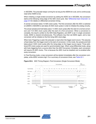
Figure 22-3. ADC Prescaler
ADEN
START
Reset
7-BIT ADC PRESCALER
CK/64
CK/128
CK/32
CK/8
CK/16
CK/4
CK/2
CK
ADPS0
ADPS1
ADPS2
ADC CLOCK SOURCE
By default, the successive approximation circuitry requires an input clock frequency between 50
kHz and 200 kHz to get maximum resolution. If a lower resolution than 10 bits is needed, the
input clock frequency to the ADC can be higher than 200 kHz to get a higher sample rate.
The ADC module contains a prescaler, which generates an acceptable ADC clock frequency
from any CPU frequency above 100 kHz. The prescaling is set by the ADPS bits in ADCSRA.
The prescaler starts counting from the moment the ADC is switched on by setting the ADEN bit
210
ATmega16A
8154A–AVR–06/08](https://image.slidesharecdn.com/atmega16a-140118085558-phpapp02/85/A-tmega16A-Microcontroller-Data-Sheet-210-320.jpg)
![ATmega16A
• ADC9:0: ADC Conversion Result
These bits represent the result from the conversion, as detailed in “ADC Conversion Result” on
page 219.
22.9.4
SFIOR – Special FunctionIO Register
Bit
7
6
5
4
3
2
1
0
ADTS2
ADTS1
ADTS0
–
ACME
PUD
PSR2
PSR10
Read/Write
R/W
R/W
R/W
R
R/W
R/W
R/W
R/W
Initial Value
0
0
0
0
0
0
0
0
SFIOR
• Bit 7:5 – ADTS2:0: ADC Auto Trigger Source
If ADATE in ADCSRA is written to one, the value of these bits selects which source will trigger
an ADC conversion. If ADATE is cleared, the ADTS2:0 settings will have no effect. A conversion
will be triggered by the rising edge of the selected Interrupt Flag. Note that switching from a trigger source that is cleared to a trigger source that is set, will generate a positive edge on the
trigger signal. If ADEN in ADCSRA is set, this will start a conversion. Switching to Free Running
mode (ADTS[2:0]=0) will not cause a trigger event, even if the ADC Interrupt Flag is set.
Table 22-6.
ADC Auto Trigger Source Selections
ADTS2
ADTS1
ADTS0
Trigger Source
0
0
0
Free Running mode
0
0
1
Analog Comparator
0
1
0
External Interrupt Request 0
0
1
1
Timer/Counter0 Compare Match
1
0
0
Timer/Counter0 Overflow
1
0
1
Timer/Counter1 Compare Match B
1
1
0
Timer/Counter1 Overflow
1
1
1
Timer/Counter1 Capture Event
• Bit 4 – Res: Reserved Bit
This bit is reserved for future use. To ensure compatibility with future devices, this bit must be
written to zero when SFIOR is written.
225
8154A–AVR–06/08](https://image.slidesharecdn.com/atmega16a-140118085558-phpapp02/85/A-tmega16A-Microcontroller-Data-Sheet-225-320.jpg)
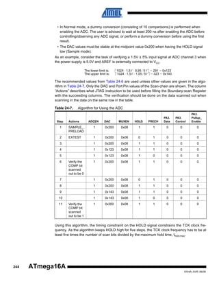
![ATmega16A
Table 24-6.
Boundary-scan Signals for the ADC (Continued)
Recommended
Input when Not
in Use
Output Values when Recommended
Inputs are used, and CPU is not
Using the ADC
Input Mux bit 3
0
0
Input
Input Mux bit 2
0
0
MUXEN_1
Input
Input Mux bit 1
0
0
MUXEN_0
Input
Input Mux bit 0
1
1
NEGSEL_2
Input
Input Mux for negative input for
differential signal, bit 2
0
0
NEGSEL_1
Input
Input Mux for negative input for
differential signal, bit 1
0
0
NEGSEL_0
Input
Input Mux for negative input for
differential signal, bit 0
0
0
PASSEN
Input
Enable pass-gate of gain stages.
1
1
PRECH
Input
Precharge output latch of
comparator. (Active low)
1
1
SCTEST
Input
Switch-cap TEST enable. Output
from x10 gain stage send out to
Port Pin having ADC_4
0
0
ST
Input
Output of gain stages will settle
faster if this signal is high first two
ACLK periods after AMPEN goes
high.
0
0
VCCREN
Input
Selects Vcc as the ACC reference
voltage.
0
0
Signal
Name
Direction as Seen
from the ADC
Description
MUXEN_3
Input
MUXEN_2
Note:
Incorrect setting of the switches in Figure 24-10 will make signal contention and may damage the part. There are several input
choices to the S&H circuitry on the negative input of the output comparator in Figure 24-10. Make sure only one path is selected
from either one ADC pin, Bandgap reference source, or Ground.
If the ADC is not to be used during scan, the recommended input values from Table 24-6 should
be used. The user is recommended not to use the Differential Gain stages during scan. Switchcap based gain stages require fast operation and accurate timing which is difficult to obtain
when used in a scan chain. Details concerning operations of the differential gain stage is therefore not provided.
The AVR ADC is based on the analog circuitry shown in Figure 24-10 with a successive approximation algorithm implemented in the digital logic. When used in Boundary-scan, the problem is
usually to ensure that an applied analog voltage is measured within some limits. This can easily
be done without running a successive approximation algorithm: apply the lower limit on the digital DAC[9:0] lines, make sure the output from the comparator is low, then apply the upper limit
on the digital DAC[9:0] lines, and verify the output from the comparator to be high.
The ADC need not be used for pure connectivity testing, since all analog inputs are shared with
a digital port pin as well.
When using the ADC, remember the following:
• The Port Pin for the ADC channel in use must be configured to be an input with pull-up
disabled to avoid signal contention.
243
8154A–AVR–06/08](https://image.slidesharecdn.com/atmega16a-140118085558-phpapp02/85/A-tmega16A-Microcontroller-Data-Sheet-243-320.jpg)
![ATmega16A
Figure 25-3. Addressing the Flash during SPM(1)
BIT
15
ZPCMSB
ZPAGEMSB
Z - REGISTER
1 0
0
PCMSB
PROGRAM
COUNTER
PAGEMSB
PCPAGE
PCWORD
PAGE ADDRESS
WITHIN THE FLASH
WORD ADDRESS
WITHIN A PAGE
PROGRAM MEMORY
PAGE
PAGE
INSTRUCTION WORD
PCWORD[PAGEMSB:0]:
00
01
02
PAGEEND
Notes:
25.8
1. The different variables used in Figure 25-3 are listed in Table 25-8 on page 263.
2. PCPAGE and PCWORD are listed in Table 26-5 on page 267.
Self-Programming the Flash
The program memory is updated in a page by page fashion. Before programming a page with
the data stored in the temporary page buffer, the page must be erased. The temporary page buffer is filled one word at a time using SPM and the buffer can be filled either before the page
erase command or between a page erase and a page write operation:
Alternative 1, fill the buffer before a Page Erase
• Fill temporary page buffer
• Perform a Page Erase
• Perform a Page Write
Alternative 2, fill the buffer after Page Erase
• Perform a Page Erase
• Fill temporary page buffer
• Perform a Page Write
If only a part of the page needs to be changed, the rest of the page must be stored (for example
in the temporary page buffer) before the erase, and then be rewritten. When using alternative 1,
the Boot Loader provides an effective Read-Modify-Write feature which allows the user software
to first read the page, do the necessary changes, and then write back the modified data. If alternative 2 is used, it is not possible to read the old data while loading since the page is already
erased. The temporary page buffer can be accessed in a random sequence. It is essential that
the page address used in both the page erase and page write operation is addressing the same
257
8154A–AVR–06/08](https://image.slidesharecdn.com/atmega16a-140118085558-phpapp02/85/A-tmega16A-Microcontroller-Data-Sheet-257-320.jpg)
![ATmega16A
Table 25-8.
Explanation of Different Variables used in Figure 25-3 and the Mapping to the Zpointer
Corresponding
Z-value(1)
Variable
Description
12
Most significant bit in the Program Counter. (The
Program Counter is 13 bits PC[12:0])
5
PCMSB
Most significant bit which is used to address the
words within one page (64 words in a page requires
6 bits PC [5:0]).
PAGEMSB
Z13
Bit in Z-register that is mapped to PCMSB. Because
Z0 is not used, the ZPCMSB equals PCMSB + 1.
Z6
Bit in Z-register that is mapped to PAGEMSB.
Because Z0 is not used, the ZPAGEMSB equals
PAGEMSB + 1.
PC[12:6]
Z13:Z7
Program Counter page address: Page select, for
Page Erase and Page Write
PC[5:0]
Z6:Z1
Program Counter word address: Word select, for
filling temporary buffer (must be zero during page
write operation)
ZPCMSB
ZPAGEMSB
PCPAGE
PCWORD
Note:
1. Z15:Z14: always ignored
Z0: should be zero for all SPM commands, byte select for the LPM instruction.
See “Addressing the Flash during Self-Programming” on page 256 for details about the use of
Z-pointer during Self-Programming.
263
8154A–AVR–06/08](https://image.slidesharecdn.com/atmega16a-140118085558-phpapp02/85/A-tmega16A-Microcontroller-Data-Sheet-263-320.jpg)
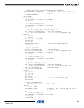
![ATmega16A
26.5
Page Size
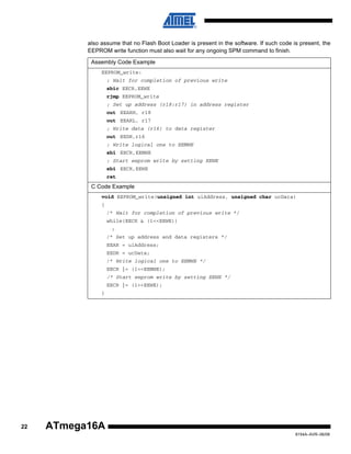
Table 26-5.
No. of Words in a Page and no. of Pages in the Flash
Flash Size
8K words (16K bytes)
Table 26-6.
Page Size
PCWORD
No. of Pages
PCPAGE
PCMSB
64 words
PC[5:0]
128
PC[12:6]
12
No. of Words in a Page and no. of Pages in the EEPROM
EEPROM Size
PCWORD
No. of Pages
PCPAGE
EEAMSB
512 bytes
26.6
Page Size
4 bytes
EEA[1:0]
128
EEA[8:2]
8
Parallel Programming Parameters, Pin Mapping, and Commands
This section describes how to parallel program and verify Flash Program memory, EEPROM
Data memory, Memory Lock bits, and Fuse bits in the ATmega16A. Pulses are assumed to be at
least 250 ns unless otherwise noted.
26.6.1
Signal Names
In this section, some pins of the ATmega16A are referenced by signal names describing their
functionality during parallel programming, see Figure 26-1 and Table 26-7. Pins not described in
the following table are referenced by pin names.
The XA1/XA0 pins determine the action executed when the XTAL1 pin is given a positive pulse.
The bit coding is shown in Table 26-9.
When pulsing WR or OE, the command loaded determines the action executed. The different
Commands are shown in Table 26-10.
Figure 26-1. Parallel Programming
+5V
RDY/BSY
PD1
OE
PD2
WR
PD3
BS1
PD4
XA0
PD6
PAGEL
+5V
PD5
XA1
VCC
PD7
+12 V
BS2
AVCC
PB7 - PB0
DATA
RESET
PA0
XTAL1
GND
267
8154A–AVR–06/08](https://image.slidesharecdn.com/atmega16a-140118085558-phpapp02/85/A-tmega16A-Microcontroller-Data-Sheet-267-320.jpg)
![Table 26-7.
Pin Name Mapping
Signal Name in
Programming Mode
Pin Name
I/O
Function
RDY/BSY
PD1
O
0: Device is busy programming, 1: Device is ready for
new command
OE
PD2
I
Output Enable (Active low)
WR
PD3
I
Write Pulse (Active low)
BS1
PD4
I
Byte Select 1 (“0” selects Low byte, “1” selects High
byte)
XA0
PD5
I
XTAL Action Bit 0
XA1
PD6
I
XTAL Action Bit 1
PAGEL
PD7
I
Program Memory and EEPROM data Page Load
BS2
PA0
I
Byte Select 2 (“0” selects Low byte, “1” selects 2’nd
High byte)
DATA
PB7-0
I/O
Table 26-8.
Bidirectional Data bus (Output when OE is low)
Pin Values used to Enter Programming Mode
Pin
Symbol
Value
PAGEL
Prog_enable[3]
0
XA1
Prog_enable[2]
0
XA0
Prog_enable[1]
0
BS1
Prog_enable[0]
0
Table 26-9.
XA1 and XA0 Coding
XA1
XA0
Action when XTAL1 is Pulsed
0
0
Load Flash or EEPROM Address (High or low address byte determined by BS1)
0
1
Load Data (High or Low data byte for Flash determined by BS1)
1
0
Load Command
1
1
No Action, Idle
Table 26-10. Command Byte Bit Coding
Command Byte
Command Executed
1000 0000
0100 0000
Write Fuse Bits
0010 0000
Write Lock Bits
0001 0000
Write Flash
0001 0001
268
Chip Erase
Write EEPROM
ATmega16A
8154A–AVR–06/08](https://image.slidesharecdn.com/atmega16a-140118085558-phpapp02/85/A-tmega16A-Microcontroller-Data-Sheet-268-320.jpg)
![ATmega16A
8 bits are required to address words in the page (pagesize < 256), the most significant bit(s) in
the address Low byte are used to address the page when performing a page write.
G. Load Address High byte
1. Set XA1, XA0 to “00”. This enables address loading.
2. Set BS1 to “1”. This selects high address.
3. Set DATA = Address High byte ($00 - $FF).
4. Give XTAL1 a positive pulse. This loads the address High byte.
H. Program Page
1. Set BS1 = “0”
2. Give WR a negative pulse. This starts programming of the entire page of data.
RDY/BSY goes low.
3. Wait until RDY/BSY goes high. (See Figure 26-3 for signal waveforms)
I. Repeat B through H until the entire Flash is programmed or until all data has been
programmed.
J. End Page Programming
1. 1. Set XA1, XA0 to “10”. This enables command loading.
2. Set DATA to “0000 0000”. This is the command for No Operation.
3. Give XTAL1 a positive pulse. This loads the command, and the internal write signals
are reset.
Figure 26-2. Addressing the Flash which is Organized in Pages
PCMSB
PROGRAM
COUNTER
PAGEMSB
PCPAGE
PAGE ADDRESS
WITHIN THE FLASH
PROGRAM MEMORY
PAGE
PCWORD
WORD ADDRESS
WITHIN A PAGE
PAGE
INSTRUCTION WORD
PCWORD[PAGEMSB:0]:
00
01
02
PAGEEND
Note:
1. PCPAGE and PCWORD are listed in Table 26-5 on page 267.
271
8154A–AVR–06/08](https://image.slidesharecdn.com/atmega16a-140118085558-phpapp02/85/A-tmega16A-Microcontroller-Data-Sheet-271-320.jpg)
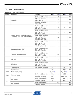
![TA = -40°C to 85°C, VCC = 2.7V to 5.5V (Unless Otherwise Noted) (Continued)
Symbol
Parameter
Condition
Min
Typ
Max
Units
Active 1 MHz, VCC = 3V
Active 4 MHz, VCC = 3V
Power Supply Current
0.6
1.9
5
mA
Active 8 MHz, VCC = 5V
7
15
mA
mA
Idle 1 MHz, VCC = 3V
0.6
2
mA
Idle 8 MHz, VCC = 5V
2.7
7
mA
WDT enabled, VCC = 3V
<8
15
µA
WDT disabled, VCC = 3V
Power-down Mode(5)
0.2
Idle 4 MHz, VCC = 3V
ICC
<1
4
µA
40
mV
50
nA
VACIO
Analog Comparator
Input Offset Voltage
VCC = 5V
Vin = VCC/2
IACLK
Analog Comparator
Input Leakage Current
VCC = 5V
Vin = VCC/2
tACPD
Analog Comparator
Propagation Delay
VCC = 2.7V
VCC = 4.0V
Notes:
-50
750
500
mA
ns
1. “Max” means the highest value where the pin is guaranteed to be read as low
2. “Min” means the lowest value where the pin is guaranteed to be read as high
3. Although each I/O port can sink more than the test conditions (20 mA at Vcc = 5V, 10 mA at Vcc = 3V) under steady state
conditions (non-transient), the following must be observed:
PDIP Package:
1] The sum of all IOL, for all ports, should not exceed 200 mA.
2] The sum of all IOL, for port A0 - A7, should not exceed 100 mA.
3] The sum of all IOL, for ports B0 - B7,C0 - C7, D0 - D7 and XTAL2, should not exceed 100 mA.
TQFP and QFN/MLF Package:
1] The sum of all IOL, for all ports, should not exceed 400 mA.
2] The sum of all IOL, for ports A0 - A7, should not exceed 100 mA.
3] The sum of all IOL, for ports B0 - B4, should not exceed 100 mA.
4] The sum of all IOL, for ports B3 - B7, XTAL2, D0 - D2, should not exceed 100 mA.
5] The sum of all IOL, for ports D3 - D7, should not exceed 100 mA.
6] The sum of all IOL, for ports C0 - C7, should not exceed 100 mA.
If IOL exceeds the test condition, VOL may exceed the related specification. Pins are not guaranteed to sink current greater
than the listed test condition.
4. Although each I/O port can source more than the test conditions (20 mA at Vcc = 5V, 10 mA at Vcc = 3V) under steady state
conditions (non-transient), the following must be observed:
PDIP Package:
1] The sum of all IOH, for all ports, should not exceed 200 mA.
2] The sum of all IOH, for port A0 - A7, should not exceed 100 mA.
3] The sum of all IOH, for ports B0 - B7,C0 - C7, D0 - D7 and XTAL2, should not exceed 100 mA.
TQFP and QFN/MLF Package:
1] The sum of all IOH, for all ports, should not exceed 400 mA.
2] The sum of all IOH, for ports A0 - A7, should not exceed 100 mA.
3] The sum of all IOH, for ports B0 - B4, should not exceed 100 mA.
4] The sum of all IOH, for ports B3 - B7, XTAL2, D0 - D2, should not exceed 100 mA.
5] The sum of all IOH, for ports D3 - D7, should not exceed 100 mA.
6] The sum of all IOH, for ports C0 - C7, should not exceed 100 mA.If IOH exceeds the test condition, VOH may exceed the
related specification. Pins are not guaranteed to source current greater than the listed test condition.
5. Minimum VCC for Power-down is 2.5V.
294
ATmega16A
8154A–AVR–06/08](https://image.slidesharecdn.com/atmega16a-140118085558-phpapp02/85/A-tmega16A-Microcontroller-Data-Sheet-294-320.jpg)

27.5
f(2)
33
Notes:
C [pF]
22
650 kHz
10
22
1. R should be in the range 3 kΩ - 100 kΩ, and C should be at least 20 pF.
2. The frequency will vary with package type and board layout.
2.0 MHz
System and Reset Characteristics
Table 27-2.
Symbol
Reset, Brown-out and Internal Voltage ReferenceCharacteristics
Typ
Max
Units
Power-on Reset Threshold
Voltage (rising)
VPOT
Parameter
Condition
Min
1.4
2.3
V
Power-on Reset Threshold
Voltage (falling)(1)
1.3
2.3
V
0.9VCC
V
1.5
µs
VRST
RESET Pin Threshold
Voltage
tRST
Minimum pulse width on
RESET Pin
Brown-out Reset Threshold
Voltage(2)
BODLEVEL = 1
2.5
2.7
3.2
VBOT
BODLEVEL = 0
3.6
4.0
4.5
Minimum low voltage period
for Brown-out Detection
BODLEVEL = 1
2
µs
tBOD
BODLEVEL = 0
2
µs
VHYST
Brown-out Detector
hysteresis
50
mV
VBG
Bandgap reference voltage
tBG
IBG
Notes:
296
0.1 VCC
V
1.15
1.23
1.4
V
Bandgap reference start-up
time
40
70
µs
Bandgap reference current
consumption
10
µA
1. The Power-on Reset will not work unless the supply voltage has been below VPOT (falling).
ATmega16A
8154A–AVR–06/08](https://image.slidesharecdn.com/atmega16a-140118085558-phpapp02/85/A-tmega16A-Microcontroller-Data-Sheet-296-320.jpg)

![29. Register Summary
Address
Name
Bit 7
Bit 6
Bit 5
Bit 4
Bit 3
Bit 2
Bit 1
Bit 0
$3F ($5F)
SREG
I
T
H
S
V
N
Z
C
9
$3E ($5E)
SPH
–
–
–
–
–
SP10
SP9
SP8
12
SP4
SP3
SP2
SP1
SP0
12
–
–
–
IVSEL
IVCE
47, 69
$3D ($5D)
SPL
$3C ($5C)
OCR0
$3B ($5B)
GICR
SP7
SP6
SP5
Timer/Counter0 Output Compare Register
INT1
INT0
Page
85
INT2
$3A ($5A)
GIFR
INTF1
INTF0
INTF2
–
–
–
–
–
69
$39 ($59)
TIMSK
OCIE2
TOIE2
TICIE1
OCIE1A
OCIE1B
TOIE1
OCIE0
TOIE0
85, 115, 134
85, 115, 134
$38 ($58)
TIFR
OCF2
TOV2
ICF1
OCF1A
OCF1B
TOV1
OCF0
TOV0
$37 ($57)
SPMCR
SPMIE
RWWSB
–
RWWSRE
BLBSET
PGWRT
PGERS
SPMEN
255
$36 ($56)
TWCR
TWINT
TWEA
TWSTA
TWSTO
TWWC
TWEN
–
TWIE
200
$35 ($55)
MCUCR
SM2
SE
SM1
SM0
ISC11
ISC10
ISC01
ISC00
36, 67
$34 ($54)
MCUCSR
JTD
ISC2
–
JTRF
WDRF
BORF
EXTRF
PORF
41, 68, 249
$33 ($53)
TCCR0
FOC0
WGM00
COM01
COM00
WGM01
CS02
CS01
CS00
82
$32 ($52)
TCNT0
$31(1) ($51)(1)
OSCCAL
OCDR
Timer/Counter0 (8 Bits)
84
Oscillator Calibration Register
31
On-Chip Debug Register
231
$30 ($50)
SFIOR
ADTS2
ADTS1
ADTS0
–
ACME
PUD
PSR2
PSR10
65,87,134,205,225
$2F ($4F)
TCCR1A
COM1A1
COM1A0
COM1B1
COM1B0
FOC1A
FOC1B
WGM11
WGM10
109
$2E ($4E)
TCCR1B
ICNC1
ICES1
–
WGM13
WGM12
CS12
CS11
CS10
112
$2D ($4D)
TCNT1H
Timer/Counter1 – Counter Register High Byte
113
$2C ($4C)
TCNT1L
113
$2B ($4B)
OCR1AH
Timer/Counter1 – Counter Register Low Byte
Timer/Counter1 – Output Compare Register A High Byte
$2A ($4A)
OCR1AL
Timer/Counter1 – Output Compare Register A Low Byte
114
$29 ($49)
OCR1BH
Timer/Counter1 – Output Compare Register B High Byte
114
114
$28 ($48)
OCR1BL
Timer/Counter1 – Output Compare Register B Low Byte
114
$27 ($47)
ICR1H
Timer/Counter1 – Input Capture Register High Byte
114
$26 ($46)
ICR1L
Timer/Counter1 – Input Capture Register Low Byte
$25 ($45)
TCCR2
$24 ($44)
TCNT2
Timer/Counter2 (8 Bits)
$23 ($43)
OCR2
Timer/Counter2 Output Compare Register
$22 ($42)
ASSR
$21 ($41)
FOC2
WGM20
COM21
114
COM20
WGM21
CS22
CS21
CS20
133
133
–
–
–
–
AS2
TCN2UB
OCR2UB
TCR2UB
WDTCR
$20(2) ($40)(2)
130
–
–
–
WDTOE
WDE
WDP2
WDP1
WDP0
UBRRH
URSEL
–
–
–
UBRR[11:8]
133
42
170
UCSRC
URSEL
UMSEL
UPM1
UPM0
USBS
UCSZ1
UCSZ0
UCPOL
169
$1F ($3F)
EEARH
–
–
–
–
–
–
–
EEAR8
19
$1E ($3E)
EEARL
EEPROM Address Register Low Byte
$1D ($3D)
EEDR
EEPROM Data Register
$1C ($3C)
EECR
–
–
–
–
EERIE
EEMWE
EEWE
EERE
$1B ($3B)
PORTA
PORTA7
PORTA6
PORTA5
PORTA4
PORTA3
PORTA2
PORTA1
PORTA0
65
$1A ($3A)
DDRA
DDA7
DDA6
DDA5
DDA4
DDA3
DDA2
DDA1
DDA0
65
65
19
20
20
$19 ($39)
PINA
PINA7
PINA6
PINA5
PINA4
PINA3
PINA2
PINA1
PINA0
$18 ($38)
PORTB
PORTB7
PORTB6
PORTB5
PORTB4
PORTB3
PORTB2
PORTB1
PORTB0
65
$17 ($37)
DDRB
DDB7
DDB6
DDB5
DDB4
DDB3
DDB2
DDB1
DDB0
65
$16 ($36)
PINB
PINB7
PINB6
PINB5
PINB4
PINB3
PINB2
PINB1
PINB0
66
$15 ($35)
PORTC
PORTC7
PORTC6
PORTC5
PORTC4
PORTC3
PORTC2
PORTC1
PORTC0
66
$14 ($34)
DDRC
DDC7
DDC6
DDC5
DDC4
DDC3
DDC2
DDC1
DDC0
66
$13 ($33)
PINC
PINC7
PINC6
PINC5
PINC4
PINC3
PINC2
PINC1
PINC0
66
$12 ($32)
PORTD
PORTD7
PORTD6
PORTD5
PORTD4
PORTD3
PORTD2
PORTD1
PORTD0
66
$11 ($31)
DDRD
DDD7
DDD6
DDD5
DDD4
DDD3
DDD2
DDD1
DDD0
66
PIND7
PIND6
PIND5
PIND4
PIND3
PIND2
PIND1
PIND0
$10 ($30)
PIND
$0F ($2F)
SPDR
SPI Data Register
66
145
$0E ($2E)
SPSR
SPIF
WCOL
–
–
–
–
–
SPI2X
144
$0D ($2D)
SPCR
SPIE
SPE
DORD
MSTR
CPOL
CPHA
SPR1
SPR0
143
$0C ($2C)
UDR
$0B ($2B)
UCSRA
$0A ($2A)
UCSRB
$09 ($29)
UBRRL
$08 ($28)
ACSR
ACD
ACBG
$07 ($27)
ADMUX
REFS1
$06 ($26)
ADCSRA
ADEN
$05 ($25)
ADCH
ADC Data Register High Byte
224
$04 ($24)
ADCL
ADC Data Register Low Byte
224
$03 ($23)
TWDR
Two-wire Serial Interface Data Register
$02 ($22)
TWAR
334
USART I/O Data Register
166
RXC
TXC
UDRE
FE
DOR
PE
U2X
MPCM
167
RXCIE
TXCIE
UDRIE
RXEN
TXEN
UCSZ2
RXB8
TXB8
168
ACO
ACI
ACIE
ACIC
ACIS1
ACIS0
205
REFS0
ADLAR
MUX4
MUX3
MUX2
MUX1
MUX0
221
ADSC
ADATE
ADIF
ADIE
ADPS2
ADPS1
ADPS0
223
USART Baud Rate Register Low Byte
TWA6
TWA5
TWA4
170
202
TWA3
TWA2
TWA1
TWA0
TWGCE
203
ATmega16A
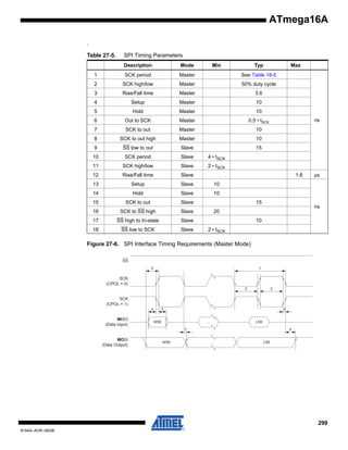
8154A–AVR–06/08](https://image.slidesharecdn.com/atmega16a-140118085558-phpapp02/85/A-tmega16A-Microcontroller-Data-Sheet-334-320.jpg)


The Atmega16A is a low-power, high-performance 8-bit microcontroller based on an advanced RISC architecture, featuring 16k bytes of in-system programmable flash memory, 512 bytes of EEPROM, and 1k bytes of SRAM. It offers a rich set of peripherals including multiple timers, serial interfaces, and an ADC, making it suitable for various embedded control applications. Additional features include programmable power-saving modes and extensive debugging support, all packaged in a highly flexible and cost-effective format.