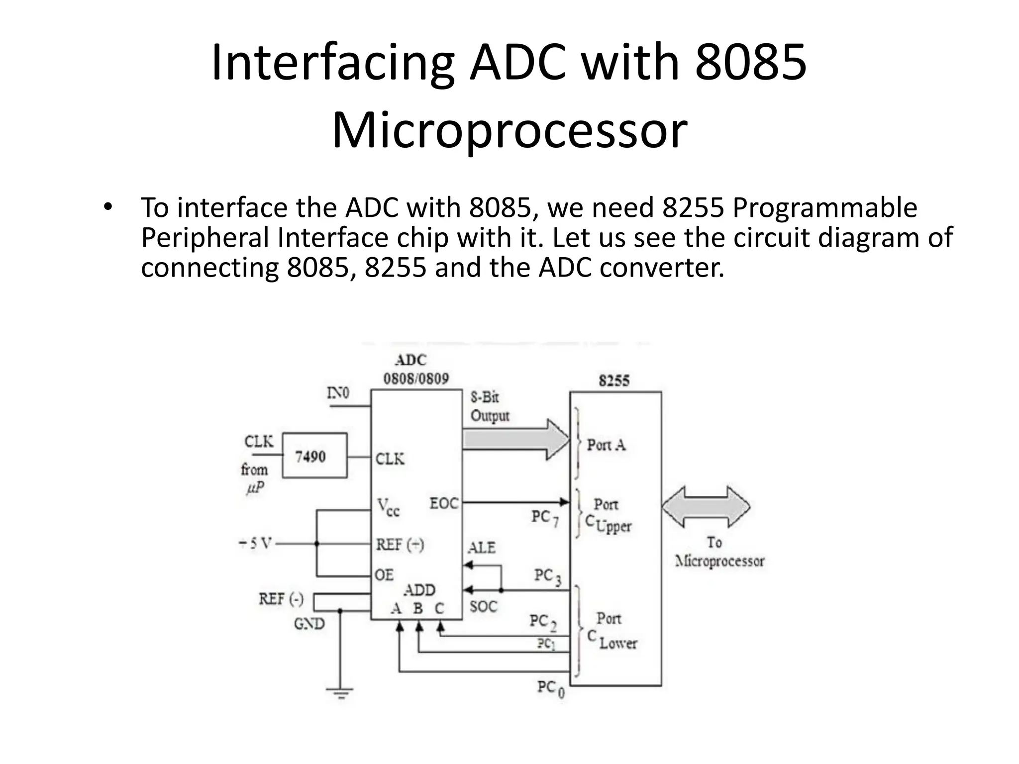
The document discusses interfacing analog to digital converters with microprocessors using the 8255 PIO. It describes how the 8255 is used to issue start of conversion pulses to the ADC and read the end of conversion and digital output signals. It provides examples of interfacing the ADC0808/0809 chip, which uses successive approximation conversion. Interfacing a digital to analog converter is also covered, with an example of interfacing the AD7523 DAC and generating an output sawtooth waveform.
analog to digital converter and dac finalDrVikasMahor
The document discusses interfacing analog to digital converters with microprocessors using an 8255 chip as an I/O port. It describes how the 8255 is used to issue start and end of conversion signals to the ADC and read the digital output. It provides examples of interfacing common ADC chips like the 0808/0809, which use successive approximation conversion. Interfacing a digital to analog converter like the AD7523 is also covered, including a program to generate a sawtooth waveform using an 8086 CPU and 8255 port.
This document describes the design of a digital voltmeter using an 8051 microcontroller and ADC0804 analog-to-digital converter. It includes the circuit diagram and explanations of the main components. The 8051 microcontroller reads the analog input voltage, converts it to a digital value using the successive approximation ADC0804, and displays the reading on an LCD screen. The document provides details on interfacing the ADC0804 and LCD, as well as the pin descriptions and timing diagrams for programming and operation. It aims to explain how to build a digital voltmeter circuit using low-cost microcontroller and ADC components.
DIGITAL VOLTMETER USING 8051 MICROCONTROLLERChirag Lakhani
This document describes the design of a digital voltmeter using an 8051 microcontroller. It includes the following key points:
- An analog to digital converter (ADC0804) is used to convert an analog input voltage to a digital signal that can be read by the microcontroller.
- The 8051 microcontroller then processes the digital signal from the ADC and displays the voltage reading on a liquid crystal display (LCD).
- The circuit diagram shows how the ADC, microcontroller, and LCD are interconnected. Key components include ports for input/output, a crystal oscillator, and voltage regulators.
- The document provides details on the pin configurations and functions of the 8051 microcontroller and ADC0804
The document discusses interfacing various peripherals to an 8086 microprocessor using an 8255 PPI chip. It describes the different modes of operation of the 8255 and provides examples of interfacing a keyboard, displays, stepper motor, DAC, and ADC. Circuit diagrams and programming examples are given for displaying numbers on a 7-segment display, generating waveforms using a DAC, and sampling an analog input with an ADC. Interfacing of peripherals like stepper motors, keyboards and displays allows microprocessors to interact with the external world.
This document describes a monitoring, protection, and control module for a radar transmitter. The module monitors key transmitter parameters, protects the system by triggering faults if parameters exceed thresholds, and controls the transmitter's on/off sequencing. It uses comparators to detect parameter faults, a microcontroller for control and interfacing, an ADC to convert analog signals, and an LCD for output display. The design aims to safely monitor and protect the expensive transmitter components.
8255-PPI MPMC text book for engineering.pptkhushiduppala
The 8259A Programmable Interrupt Controller allows for 8 interrupt inputs to be handled individually. It can prioritize interrupts and mask lower priority interrupts while higher ones are serviced. The controller's pins include data bus pins to transfer control/status information, as well as pins for chip select, read/write, cascade connections for multiple controllers, and interrupt request/acknowledge lines. It provides flexible interrupt handling capabilities for microprocessors like the 8085A and 8086.
The document discusses interfacing analog to digital converters (ADCs), digital to analog converters (DACs), and sensors with PIC18F microcontrollers. It describes the basics of AD conversion including transducers. It then discusses characteristics, registers, and programming of the PIC18F ADC. It also covers DAC concepts and interfacing a DAC0888. Finally, it discusses temperature sensors and interfacing LM34 and LM35 sensors to measure temperature.
The document discusses the Intel 8253 programmable interval timer integrated circuit. It has 3 independent 16-bit counters that can be programmed to operate in 6 different modes. The 8253 architecture includes data and control logic, a control word register, and 3 counters. It also details the pinout, provides examples of how the different timer modes work, and references for more information.
The document discusses the 8155 Programmable Peripheral Interface chip. It can be used as an interface between a microprocessor and I/O devices. The 8155 contains RAM, I/O ports, and a timer. It has ports A, B, and C that can be configured as input or output. The timer can operate in different modes. Programming the 8155 involves writing control words to its control register to configure the ports and timer. An example application shows how an 8155 can be used to interface an ADC and read temperature values using handshaking between the ADC and 8155 ports.
- Both analog data from the physical world and analog control signals must be converted to digital form to be processed by digital electronics. This involves converting signals from analog to digital and back again from digital to analog.
- There are two main approaches to digital to analog conversion: using a weighted summing amplifier or an R-2R ladder network. The R-2R network is better for higher bit conversions due to greater precision.
- There are three main types of analog to digital converters: digital ramp ADCs, successive approximation ADCs, and flash ADCs. Successive approximation ADCs are faster than digital ramp ADCs but slower than flash ADCs, which are the fastest but require the most circuitry.
This document discusses interfacing an analog-to-digital converter (ADC) and digital-to-analog converter (DAC) with an 8051 microcontroller. It describes the ADC0804 and DAC0808 integrated circuits. The ADC0804 is an 8-bit ADC that converts analog voltages to 8-bit digital values. It has a resolution of 8-bits and a maximum conversion time of 110us. The DAC0808 is an 8-bit DAC that converts digital values to an analog current. Software is provided to generate a sine wave using the DAC and control a stepper motor by interfacing it with the microcontroller ports. Programs in C are given to read the switch status and rotate
The document discusses various techniques for interfacing microcontrollers to sensors, including analog interfaces using analog-to-digital converters to read sensor output voltages and convert them to digital values. It provides examples of interfacing microcontrollers to temperature sensors like the LM34 and LM35, whose output voltage varies linearly with temperature, and to ADC0848 and ADC0804 analog-to-digital converters. The document also includes code to read temperature sensor values using an ADC0848 converter and display the results on an 8051 microcontroller's port pins.
The document provides an overview of programmable logic controllers (PLCs). It defines PLCs as digital electronic devices that use programmable memory to implement logic functions like sequencing and timing to control machines and processes. The document discusses the basic structure of PLCs including the CPU, memory, input/output interfaces, and power supply. It also covers programming methods like ladder logic and instruction lists. Additional topics include input/output addressing, timers, counters, and techniques like latching, internal relays, and sequencing using timers.
The document provides information about a seminar on embedded systems using the 8051 microcontroller. It discusses the introduction to embedded systems and their components. It then describes the features and architecture of the 8051 microcontroller, including its pins, addressing modes, and timers. Examples of embedded systems are also listed. The document concludes with discussing other integrated circuits like the 8085 microprocessor, 78XX voltage regulators, L293D motor driver, LCD displays, and logic level converters like the MAX232.
Training Report on embedded Systems and RoboticsNIT Raipur
Deepak Kumar completed a training report on embedded systems and robotics at I3indya Technologies in Delhi for his vocational project in the 2012-2013 academic year. He studied topics including an overview of embedded systems, microcontrollers like the Atmega16, analog to digital conversion, timers, interfacing various components like 7-segment displays, LCDs, DC motors, sensors, and more. The 3-page report was submitted to his college, the National Institute of Technology Raipur, to fulfill requirements for his Bachelor of Technology degree.
This document provides information on peripheral interfacing in microprocessors. It discusses memory interfacing and I/O interfacing, and some of the peripheral devices developed by Intel like the 8255 parallel communication interface, 8251 serial communication interface, 8254 programmable timer, and 8257 DMA controller. It then describes serial and parallel communication interfaces. It provides details on the 8255 programmable peripheral interface and its operating modes. Finally, it discusses digital to analog converters, applications of the 8254 timer/counter, and analog to digital converters.
An analog-to-digital converter (ADC, A/D, or A to D) is a device that converts a continuous physical quantity (usually voltage) to a digital number that represents the quantity's amplitude.
The conversion involves quantization of the input, so it necessarily introduces a small amount of error. Instead of doing a single conversion, an ADC often performs the conversions ("samples" the input) periodically. The result is a sequence of digital values that have been converted from a continuous-time and continuous-amplitude analog signal to a discrete-time and discrete-amplitude digital signal.
This document provides information about the 8253 Programmable Interval Timer (PIC). It begins by explaining the data bus buffer of the 8253, which is an 8-bit bidirectional buffer that interfaces the timer to the system data bus. It then describes the read/write logic, chip select line, and address lines of the 8253. The document goes on to explain the control word register, counters, modes of operation, and internal architecture of the timers. It provides details about the clock, gate, and output pins associated with each timer.
UNIT 4 & 5 - I nterfacing_Lecture7.pptxnaveen088888
The document discusses analog sensor interfacing and analog to digital conversion. It explains that physical quantities in the real world are analog while computers use digital values, so an analog to digital converter (ADC) is used to convert analog sensor signals to digital values. It then describes the characteristics of ADCs like resolution, conversion time, reference voltage, and output data format. It provides examples of calculating the step size and digital output for different resolutions and reference voltages. Finally, it discusses different types of sensors, interfacing techniques for sensors, displays, and relays with microcontrollers.
The 8254 programmable interval timer consists of three independent 16-bit programmable counters that can each count in binary or BCD up to a maximum frequency of 10 MHz. This timer is useful for controlling real-time events in microprocessors. In personal computers, the timer generates an 18.2 Hz interrupt, refreshes DRAM memory, and provides timing to devices like speakers. Each counter has inputs and outputs to control counting. The 8254 has various modes to generate pulses, squares waves, and one-shots using the counters.
The 8259A is an interrupt controller that manages interrupt requests from peripheral devices connected to a microprocessor. It has 8 interrupt request lines that accept signals from devices. The 8259A prioritizes the interrupt requests, masks some if needed, and issues an interrupt signal to the CPU. It then provides the CPU with the address of the interrupt service routine for the highest priority active interrupt by placing the address bytes on the data bus over 3 interrupt acknowledge pulses from the CPU. This allows efficient interrupt-driven processing of device requests.
Interfacing with Timer IC.pptx interfacing with timer icSunilAcharya37
The document discusses interfacing with timers and counters using the Intel 8253/8254 Programmable Interval Timer chip. It provides information on the timer modes, programming the chip, and examples of using counters 0 and 1 to generate pulses and square waves. Specifically, it shows:
1) The 8254 timer chip has three 16-bit counters that can be programmed to operate in six different modes to generate time delays, pulses, and digital waveforms.
2) Examples are given to initialize counter 2 to count down from 50,000 in mode 0 and generate a 50us pulse from counter 0 in mode 2.
3) A third example shows how to program counter 1 to generate a 1kHz
MicroProcessors and MicroControllersUnit3deepakdmaat
This document provides an overview of Unit III - I/O Interfacing in a syllabus. It discusses various topics related to interfacing memory and I/O devices, including parallel communication interfaces like the 8255 PPI chip, serial communication interfaces like the 8251 USART, and analog interfaces such as A/D converters, D/A converters, and timers. It also lists some case studies and applications that will be covered, including traffic light control, LED displays, LCD displays, keyboard/display interfaces, and alarm controllers.
The document discusses various peripherals that can be interfaced with microcontrollers, including the 8255 Programmable Peripheral Interface (PPI), ADC0809 analog to digital converter, DAC0800 digital to analog converter, and serial communication standards like RS-232. It provides details on the architecture and interfacing of the 8255 PPI and describes how its ports are selected and programmed. It also provides interfacing diagrams and example programs for interfacing the 8255 with an 8051 microcontroller, as well as for interfacing the ADC0809 and DAC0800 for analog to digital and digital to analog conversion respectively. Finally, it discusses serial communication standards like RS-232, RS-485, RS-
ijfij fi fjijfij fijfijif if iji j iijfij fi fjijfij fijfijif if iji j iijfij fi fjijfij fijfijif if iji j iijfij fi fjijfij fijfijif if iji j iijfij fi fjijfij fijfijif if iji j iijfij fi fjijfij fijfijif if iji j iijfij fi fjijfij fijfijif if iji j iijfij fi fjijfij fijfijif if iji j iijfij fi fjijfij fijfijif if iji j iijfij fi fjijfij fijfijif if iji j iijfij fi fjijfij fijfijif if iji j iijfij fi fjijfij fijfijif if iji j iijfij fi fjijfij fijfijif if iji j iijfij fi fjijfij fijfijif if iji j iijfij fi fjijfij fijfijif if iji j iijfij fi fjijfij fijfijif if iji j iijfij fi fjijfij fijfijif if iji j iijfij fi fjijfij fijfijif if iji j iijfij fi fjijfij fijfijif if iji j iijfij fi fjijfij fijfijif if iji j iijfij fi fjijfij fijfijif if iji j iijfij fi fjijfij fijfijif if iji j iijfij fi fjijfij fijfijif if iji j iijfij fi fjijfij fijfijif if iji j iijfij fi fjijfij fijfijif if iji j iijfij fi fjijfij fijfijif if iji j iijfij fi fjijfij fijfijif if iji j iijfij fi fjijfij fijfijif if iji j iijfij fi fjijfij fijfijif if iji j iijfij fi fjijfij fijfijif if iji j iijfij fi fjijfij fijfijif if iji j iijfij fi fjijfij fijfijif if iji j iijfij fi fjijfij fijfijif if iji j iijfij fi fjijfij fijfijif if iji j iijfij fi fjijfij fijfijif if iji j iijfij fi fjijfij fijfijif if iji j iijfij fi fjijfij fijfijif if iji j iijfij fi fjijfij fijfijif if iji j iijfij fi fjijfij fijfijif if iji j iijfij fi fjijfij fijfijif if iji j iijfij fi fjijfij fijfijif if iji j iijfij fi fjijfij fijfijif if iji j iijfij fi fjijfij fijfijif if iji j iijfij fi fjijfij fijfijif if iji j iijfij fi fjijfij fijfijif if iji j iijfij fi fjijfij fijfijif if iji j iijfij fi fjijfij fijfijif if iji j i
Similar to Interfacing Analog to Digital Data Converters ee3404.pdf (20)
ACEP Magazine edition 4th launched on 05.06.2024Rahul
This document provides information about the third edition of the magazine "Sthapatya" published by the Association of Civil Engineers (Practicing) Aurangabad. It includes messages from current and past presidents of ACEP, memories and photos from past ACEP events, information on life time achievement awards given by ACEP, and a technical article on concrete maintenance, repairs and strengthening. The document highlights activities of ACEP and provides a technical educational article for members.
A review on techniques and modelling methodologies used for checking electrom...nooriasukmaningtyas
The proper function of the integrated circuit (IC) in an inhibiting electromagnetic environment has always been a serious concern throughout the decades of revolution in the world of electronics, from disjunct devices to today’s integrated circuit technology, where billions of transistors are combined on a single chip. The automotive industry and smart vehicles in particular, are confronting design issues such as being prone to electromagnetic interference (EMI). Electronic control devices calculate incorrect outputs because of EMI and sensors give misleading values which can prove fatal in case of automotives. In this paper, the authors have non exhaustively tried to review research work concerned with the investigation of EMI in ICs and prediction of this EMI using various modelling methodologies and measurement setups.
DEEP LEARNING FOR SMART GRID INTRUSION DETECTION: A HYBRID CNN-LSTM-BASED MODELgerogepatton
As digital technology becomes more deeply embedded in power systems, protecting the communication
networks of Smart Grids (SG) has emerged as a critical concern. Distributed Network Protocol 3 (DNP3)
represents a multi-tiered application layer protocol extensively utilized in Supervisory Control and Data
Acquisition (SCADA)-based smart grids to facilitate real-time data gathering and control functionalities.
Robust Intrusion Detection Systems (IDS) are necessary for early threat detection and mitigation because
of the interconnection of these networks, which makes them vulnerable to a variety of cyberattacks. To
solve this issue, this paper develops a hybrid Deep Learning (DL) model specifically designed for intrusion
detection in smart grids. The proposed approach is a combination of the Convolutional Neural Network
(CNN) and the Long-Short-Term Memory algorithms (LSTM). We employed a recent intrusion detection
dataset (DNP3), which focuses on unauthorized commands and Denial of Service (DoS) cyberattacks, to
train and test our model. The results of our experiments show that our CNN-LSTM method is much better
at finding smart grid intrusions than other deep learning algorithms used for classification. In addition,
our proposed approach improves accuracy, precision, recall, and F1 score, achieving a high detection
accuracy rate of 99.50%.
Redefining brain tumor segmentation: a cutting-edge convolutional neural netw...IJECEIAES
Medical image analysis has witnessed significant advancements with deep learning techniques. In the domain of brain tumor segmentation, the ability to
precisely delineate tumor boundaries from magnetic resonance imaging (MRI)
scans holds profound implications for diagnosis. This study presents an ensemble convolutional neural network (CNN) with transfer learning, integrating
the state-of-the-art Deeplabv3+ architecture with the ResNet18 backbone. The
model is rigorously trained and evaluated, exhibiting remarkable performance
metrics, including an impressive global accuracy of 99.286%, a high-class accuracy of 82.191%, a mean intersection over union (IoU) of 79.900%, a weighted
IoU of 98.620%, and a Boundary F1 (BF) score of 83.303%. Notably, a detailed comparative analysis with existing methods showcases the superiority of
our proposed model. These findings underscore the model’s competence in precise brain tumor localization, underscoring its potential to revolutionize medical
image analysis and enhance healthcare outcomes. This research paves the way
for future exploration and optimization of advanced CNN models in medical
imaging, emphasizing addressing false positives and resource efficiency.
Using recycled concrete aggregates (RCA) for pavements is crucial to achieving sustainability. Implementing RCA for new pavement can minimize carbon footprint, conserve natural resources, reduce harmful emissions, and lower life cycle costs. Compared to natural aggregate (NA), RCA pavement has fewer comprehensive studies and sustainability assessments.
Batteries -Introduction – Types of Batteries – discharging and charging of battery - characteristics of battery –battery rating- various tests on battery- – Primary battery: silver button cell- Secondary battery :Ni-Cd battery-modern battery: lithium ion battery-maintenance of batteries-choices of batteries for electric vehicle applications.
Fuel Cells: Introduction- importance and classification of fuel cells - description, principle, components, applications of fuel cells: H2-O2 fuel cell, alkaline fuel cell, molten carbonate fuel cell and direct methanol fuel cells.
A SYSTEMATIC RISK ASSESSMENT APPROACH FOR SECURING THE SMART IRRIGATION SYSTEMSIJNSA Journal
The smart irrigation system represents an innovative approach to optimize water usage in agricultural and landscaping practices. The integration of cutting-edge technologies, including sensors, actuators, and data analysis, empowers this system to provide accurate monitoring and control of irrigation processes by leveraging real-time environmental conditions. The main objective of a smart irrigation system is to optimize water efficiency, minimize expenses, and foster the adoption of sustainable water management methods. This paper conducts a systematic risk assessment by exploring the key components/assets and their functionalities in the smart irrigation system. The crucial role of sensors in gathering data on soil moisture, weather patterns, and plant well-being is emphasized in this system. These sensors enable intelligent decision-making in irrigation scheduling and water distribution, leading to enhanced water efficiency and sustainable water management practices. Actuators enable automated control of irrigation devices, ensuring precise and targeted water delivery to plants. Additionally, the paper addresses the potential threat and vulnerabilities associated with smart irrigation systems. It discusses limitations of the system, such as power constraints and computational capabilities, and calculates the potential security risks. The paper suggests possible risk treatment methods for effective secure system operation. In conclusion, the paper emphasizes the significant benefits of implementing smart irrigation systems, including improved water conservation, increased crop yield, and reduced environmental impact. Additionally, based on the security analysis conducted, the paper recommends the implementation of countermeasures and security approaches to address vulnerabilities and ensure the integrity and reliability of the system. By incorporating these measures, smart irrigation technology can revolutionize water management practices in agriculture, promoting sustainability, resource efficiency, and safeguarding against potential security threats.
Understanding Inductive Bias in Machine LearningSUTEJAS
This presentation explores the concept of inductive bias in machine learning. It explains how algorithms come with built-in assumptions and preferences that guide the learning process. You'll learn about the different types of inductive bias and how they can impact the performance and generalizability of machine learning models.
The presentation also covers the positive and negative aspects of inductive bias, along with strategies for mitigating potential drawbacks. We'll explore examples of how bias manifests in algorithms like neural networks and decision trees.
By understanding inductive bias, you can gain valuable insights into how machine learning models work and make informed decisions when building and deploying them.
Interfacing Analog to Digital Data Converters ee3404.pdf
1. Analog to Digital Converters &
Digital to Analog Converters
EE3404 MICROPROCESSOR &
MICROCONTROLLER
2. Interfacing Analog to Digital Data
Converters
• The Analog to Digital Conversion is a
quantizing process. Here the analog signal is
represented by equivalent binary states. The
A/D converters can be classified into two
groups based on their conversion techniques.
In the first technique it compares given analog
signal with the initially generated equivalent
signal.
3. • In this technique, it includes successive
approximation, counter and flash type
converters. In another technique it determines
the changing of analog signals into time or
frequency. This process includes integrator-
converters and voltage-tofrequency converters.
The first process is faster but less accurate, the
second one is more accurate. As the first process
uses flash type, so it is expensive and difficult to
design for high accuracy.
4. ADC 0808/0809 Chip
• The ADC 0808/0809 is an 8-bit analog to digital
converter. It has 8 channel multiplexer to
interface with the microprocessor. This chip is
popular and widely used ADC. ADC 0808/0809 is
a monolithic CMOS device. This device uses
successive approximation technique to convert
analog signal to digital form. One of the main
advantage of this chip is that it does not require
any external zero and full scale adjustment, only
+5V DC supply is sufficient.
5. Features of ADC 0808/0809
• The conversion speed is much higher The
accuracy is also high It has minimal
temperature dependence Excellent long term
accuracy and repeatability Less power
consumption
7. Interfacing ADC with 8085
Microprocessor
• To interface the ADC with 8085, we need 8255 Programmable
Peripheral Interface chip with it. Let us see the circuit diagram of
connecting 8085, 8255 and the ADC converter.
8. • The PortA of 8255 chip is used as the input port. The
PC7 pin of Port Cupper is connected to the End of
Conversion (EOC) Pin of the analog to digital converter.
• This port is also used as input port. The Clower port is
used as output port. The PC2-0 lines are connected to
three address pins of this chip to select input channels.
The PC3 pin is connected to the Start of Conversion
(SOC) pin and ALE pin of ADC 0808/0809. Now let us
see a program to generate digital signal from analog
data. We are using IN0 as input pin, so the pin selection
value will be 00H
9. Digital-to-Analog Converter
• The DAC will accept a digital (binary) input and convert to
analog voltage or current.
• Every DAC will have "n" input lines and an analog output.
The DAC require a reference analog voltage (Vref) or
current (Iref) source. The smallest possible analog value
that can be represented by the n-bit binary code is called
resolution.
• The resolution of DAC with n-bit binary input is 1/2nof
reference analog value. The DAC0800 is an 8-bit, high
speed, current output DAC with a typical settling time
(conversion time) of 100 ns. It produces complementary
current output, which can be converted to voltage by using
simple resistor load. The DAC0800 require a positive and a
negative supply voltage in the range of ± 5V to ±18V
10. Digital-to-Analog Converter
• It can be directly interfaced with TTL, CMOS, PMOS and other logic
families. For TTL input, the threshold pin should be tied to ground
(VLC = 0V). The reference voltage and the digital input will decide
the analog output current, which can be converted to a voltage by
simply connecting a resistor to output terminal or by using an op-
amp I to V converter. The DAC0800 is available as a 16-pin IC in DIP.
12. IC 8253/54 - Programmable Interval
Timer
• The 8254 programmable interval
timer/counter is used to generate accurate
time delays and can be used for applications
such as a real-time clock, an event counter, a
digital one-shot, a square-wave generator, and
a complex waveform generator. The 8254
includes three identical 16-bit counters that
can operate independently in any one of the
six modes (to be described later).
13. • It is packaged in a 24-pin DIP and requires a
single +5 V power supply. To operate a
counter, a 16-bit count is loaded in its register
and, on command, begins to decrement the
count until it reaches 0. At the end of the
count it generates a pulse that can be used to
interrupt the MPU. The counter can count
either in binary or BCD. In addition, a count
can be read by the MPU while the counter is
decrementing.
15. • DATA BUS BUFFER This tri-state, 8-bit,
bidirectional buffer is connected to the data
bus of the MPU.
• CONTROL LOGIC The control section has five
signals: RD (Read), WR (Write), CS (Chip
Select) and address lines A0,A1.
16. • CONTROL WORD REGISTER This register is
accessed when lines A0 and A1 are at logic 1.
It is used to write a command word which
specifies the counter to be used, its mode,
and either a Read or a Write operation. The
control word format
17. MODES
• The 8254 can operate in six different modes, and the gate of a counter is used either to disable or enable
counting, as shown in Figure 7.3. However, to maintain clarity, only one mode (Mode 0) is illustrated first, and
details of the remaining modes are discussed in a coming section. In Mode 0, after the count is written and if
the gate is high, the count is decremented every clock cycle. When the count reaches zero; the output goes
high and remains high until a new count or mode word is loaded.
18. Programming the 8254
• The 8254 can be programmed to provide various types
of output through Write operations, or to check a
count while counting through Read operations.
19. • WRITE OPERATIONS To initialize a counter, the following steps are necessary. 1.
Write a control word into the control register. 2. Load the low-order byte of a
count in the counter register. 3. Load the high-order byte of a count in the counter
register. With a clock and an appropriate gate signal to one of the counters, the
above steps should start the counter and provide appropriate output according to
the control word. READ OPERATIONS In some applications, especially in event
counters, it is necessary to read the value of the count in progress. This can be
done by either of two methods. One method involves reading a count after
inhibiting (stopping) the counter to be read. The, second method involves reading
a count while the count is in progress (known as reading on the fly). In the first
method, counting is stopped (or inhibited) by controlling the gate input or the
clock input of the selected counter, and two IO read operations are performed by
the MPU. The first IO operation reads the low-order byte, and the second IO
operation reads the high-order byte. In the second method, an appropriate control
word is written into the control register to latch a count in the output latch, and
two IO Read operations are performed by the MPU. These Read/Write operations
are illustrated below
20. The 8254 as a Counter
• It can be directly interfaced with TTL, CMOS, PMOS and other logic
families. For TTL input, the threshold pin should be tied to ground
(VLC = 0V). The reference voltage and the digital input will decide
the analog output current, which can be converted to a voltage by
simply connecting a resistor to output terminal or by using an op-
amp I to V converter. The DAC0800 is available as a 16-pin IC in DIP.