Download as PDF, PPTX

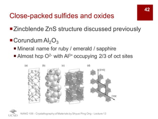
![Interaction of electrons with crystal
lattices
¡ Strong interactions with both electron clouds and positively charged
nuclei
¡ Probability of scattering of electron beam is ~ four times higher than
for X-rays
¡ Electron scattering factor can be related to the X-ray scattering factor
by the Moth-Bethe formula:
¡ High probability of scattering leads to multiple scattering events
(dynamic scattering) è electron scattering must be treated with
dynamic scattering theory
NANO 106 - Crystallography ofMaterials by Shyue Ping Ong - Lecture 13
f el
(s) =
e
16π 2
ε0 s
2
[Z − f X
(s)] where s =
sinθ
λ
9](https://image.slidesharecdn.com/13-otherdiffractiontechniques-160518164001/85/UCSD-NANO106-13-Other-Diffraction-Techniques-and-Common-Crystal-Structures-9-320.jpg)
![Atomic sizes
¡ Some metals have more than one allotrope
¡ Fe exists in bcc and fcc structures
¡ Bcc lattice constant = 2.8664 Angstroms
¡ Fcc lattice constant = 3.6468 Angstroms
¡ If we treat Fe atoms as touching spheres, we can
derive associated atomic radii for the two
structures
¡ Bcc spheres are touching along [111]
¡ Fcc spheres are touching along [110]
¡ ~4% larger radius for fcc
NANO 106 - Crystallography ofMaterials by Shyue Ping Ong - Lecture 13
4rbcc = a2
+ a2
+ a2
→ rbcc =
3a
4
=1.242nm
4rfcc = a2
+ a2
→ rfcc =
2a
4
=1.289nm
28](https://image.slidesharecdn.com/13-otherdiffractiontechniques-160518164001/85/UCSD-NANO106-13-Other-Diffraction-Techniques-and-Common-Crystal-Structures-28-320.jpg)

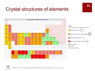
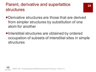
The document discusses various diffraction techniques used to determine crystal structures, including X-ray diffraction (XRD), electron diffraction, and neutron diffraction. It provides details on each technique, such as the wavelength used, how the beams interact with materials, and common applications. Neutron diffraction is described as penetrating deeply into materials and providing information on magnetic structures. Examples of common crystal structures are also presented, such as face-centered cubic and hexagonal close-packed structures. Interstitial sites and packing fractions are discussed for relating structure to properties of materials.