Downloaded 16 times
![Hall Effect in Semiconductors ( S.O. Kasap, 1990 - 2001)
An e-Booklet
3
so that Equation (4) becomes,
ev
e ev Bhy
h
y hx z
µ
= −E
ev
e ev Bey
e
y ex z
µ
= +E
where vhy and vey are the hole and electron drift velocities along y. Substituting vhx = µhEx and vex = µeEx,
these become
v
Bhy
h
y h x z
µ
µ= −E E
v
Bey
e
y e x z
µ
µ= +E E (5)
From Equation (5) we can substitute for vhy and vey in Equation (3) to obtain
pµhEy − pµh
2
Ex Bz = −nµeEy − nµe
2
ExBz
or Ey(pµh + nµe) = BzEx(pµh
2
− nµe
2
) (6)
We now consider what happens along the x-direction. The total current density is finite and is given
by the usual expression,
Jx = epvhx + envex = (pµh + nµe)eEx (7)
We can use Equation (7) to substitute for Ex in Equation (6), to obtain
eEy(nµe + pµh)2
= BzJx(pµh
2
− nµe
2
)
The Hall coefficient, by definition, is RH = Ey/JxBz so that
R
p n
e p n
H
h e
h e
=
−
+( )
µ µ
µ µ
2 2
2 Hall Effect for ambipolar conduction (8)
or R
p nb
e p nb
H =
−
+( )
2
2 Hall Effect for ambipolar conduction (9)
where b = µe/µh. It is clear that the Hall coefficient depends on both the drift mobility ratio and the
concentrations of holes and electrons. For p > nb2
, RH will be positive and for p < nb2
, it will be negative.
We should note that when only one type of carrier is involved, e.g. electrons only, Jy = 0 requirement means
that Jy = envey = 0, or vey = 0. The drift velocity along y can only be zero, if the net driving force, Fey, along y
is zero. This occurs when the Lorentz force just balances the force due to the built-in field.
1. Example: Hall coefficient of intrinsic silicon
Intrinsic silicon has electron and hole concentrations, n = p = ni =1.5 × 10¹⁰
cm-3
, and electron and hole
drift mobilities, µe = 1350 cm2
V-1
s-1
, µh = 450 cm2
V-1
s-1
. Calculate the Hall coefficient and compare it
with a typical metal.
Solution
Given n = p = ni = 1.5 × 10¹⁰
cm-3
, µe = 1350 cm2
V-1
s-1
and µh = 450 cm2
V-1
s-1
we have
b = µe/µh = 1350/450 = 3
then, RH =
× − ×
× × + ×[ ]−
( ) ( )( )
( . ) ( ) ( )( )
1 10 1 10 3
1 6 10 1 10 1 10 3
16 16 2
19 16 16 2
m m
C m m
-3 -3
-3 -3
or RH = −208 m3
A-1
s-1](https://image.slidesharecdn.com/halleffectsemicon-140517042626-phpapp02/85/The-Hall-Effect-3-320.jpg)
![Hall Effect in Semiconductors ( S.O. Kasap, 1990 - 2001)
An e-Booklet
4
which is orders of magnitude larger than that for a typical metal. All Hall effect devices use a
semiconductor rather than a metal sample.
2. Example: Zero Hall coefficient in a semiconductor
Given the mass action law, np = ni
2
, find the electron concentration when the Hall coefficient is zero for a
semiconductor. Using ni =1.5 × 10¹⁰
cm-3
, and electron and hole drift mobilities, µe = 1350 cm2
V-1
s-1
and
µh = 450 cm2
V-1
s-1
, what are n and p in Si for zero RH?
Solution
Substituting the mass action law p = ni
2
/n into Equation (9) we get
R
p nb
e p nb
n
n
nb
e
n
n
nb
H
i
i
=
−
+( )
=
−
+
=
2
2
2
2
2 2 0
that is
n
n
nbi
2
2
0− =
solving, n = ni/b = 0.33ni = 5 × 10⁹
cm-3
Obviously the corresponding hole concentration, p = bni or 4.5 × 10¹⁰
cm-3
.
3. Example: Maximum Hall coefficient in a semiconductor
Given the mass action law, np = ni
2
, find n for maximum RH (negative and positive). Assume that the drift
mobilities remain relatively unaffected as n changes (due to doping). Given the electron and hole drift
mobilities, µe = 1350 cm2
V-1
s-1
, µh = 450 cm2
V-1
s-1
for silicon, determine n for maximum RH in terms of
ni.
Solution
Substituting the mass action law p = ni
2
/n into Equation (9) we get
R
p nb
e p nb
n
n
nb
e
n
n
nb
u
v
H
i
i
=
−
+( )
=
−
+
=
2
2
2
2
2 2
where u and v represent the numerator and denominator as a function of n.
Then
dR
dn
u v uv
v
H
=
′ − ′
=2
0
where primes are derivatives with respect to n. This means that u′v − u v′ = 0, so that,
′ − ′ = − −
+
− −
+
− +
=u v uv
n
n
b e
n
n
nb
n
n
nb e
n
n
nb
n
n
bi i i i i
2
2
2
2 2 2
2
2 2
2
2 0
We can multiply through by n3
and then combine terms and factor to obtain,
b n n b b n ni i
3 4 2 2 4
3 1 0− + + =[ ( )]](https://image.slidesharecdn.com/halleffectsemicon-140517042626-phpapp02/85/The-Hall-Effect-4-320.jpg)
![Hall Effect in Semiconductors ( S.O. Kasap, 1990 - 2001)
An e-Booklet
5
or, b3
x2
+ [−3b(1−b)]x + 1 = 0
where x = (n/ni)2
. This is a quadratic equation in x. Its solution is,
x
n
n
b b b b b
bi
= =
+( ) ± +( ) −2
2
2 2 3
3
3 1 9 1 4
2
For Si, b = 3, and we have two solutions corresponding to n/ni = 1.14 and n/ni = 0.169, or p/ni =
1/0.169 = 5.92.
4. Example: Hall coefficient of a semiconductor
Given the mass action law, np = ni
2
, and the electron and hole drift mobilities, µe = 1350 cm2
V-1
s-1
, µh =
450 cm2
V-1
s-1
for silicon, that is b = 3, sketch schematically how RH changes with electron concentration n,
given those values of n resulting in RH = 0 and maximum RH values in the above examples.
Solution
Substituting the mass action law p = ni
2
/n into Equation (9) and using a normalized electron
concentration x = n/ni, we get,
R
p nb
e p nb
n
n
nb
e
n
n
nb
x
xb
en
x
xb
H
i
i
i
=
−
+( )
=
−
+
=
−
+
2
2
2
2
2 2
2
2
1
1
or y
R
en
x
xb
x
xb
H
i
=
=
−
+
1
1
1
2
2
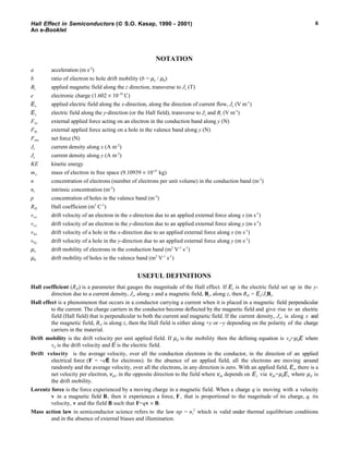
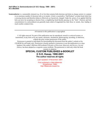
RH vs. n obviously follows y vs. x, which is shown in Figure 2 for b = 3. It is left as an exercise to
show that, when n >> ni, RH = −1/en and when n << ni, RH = +1/ep.
Normalized Hall coefficient vs. normalized electron concentration. Values
0.17, 1.14 and 0.33 shown are n/n
i
values when the magnitude of RH
reaches
maxima and zero respectively.
-0.6
-0.5
-0.4
-0.3
-0.2
-0.1
0
0.1
0.2
0.01 0.1 1 10n/ni
(eni)RH
1.14
0.17
1/3
Figure 2](https://image.slidesharecdn.com/halleffectsemicon-140517042626-phpapp02/85/The-Hall-Effect-5-320.jpg)

1. The document discusses the Hall effect in semiconductors where both electrons and holes are present as charge carriers. It describes how the Hall coefficient depends on the concentrations and mobilities of both types of carriers. 2. An example calculates the Hall coefficient of intrinsic silicon to be -208 m3/A-s, which is much larger than typical metals. 3. Another example finds that the electron concentration where the Hall coefficient is zero is 5×109 cm-3, with a corresponding hole concentration of 4.5×1010 cm-3.