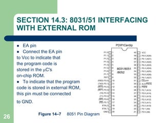
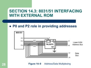
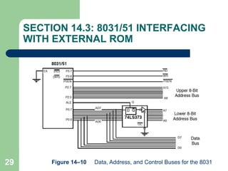
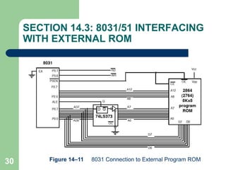
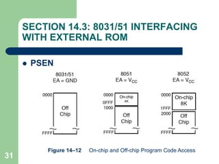
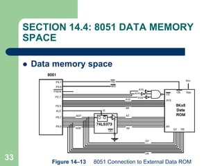
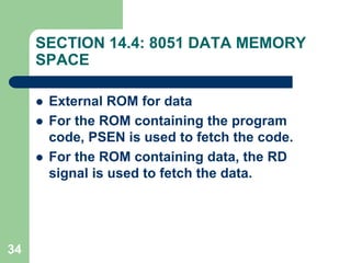
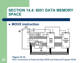
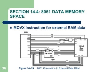
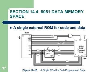
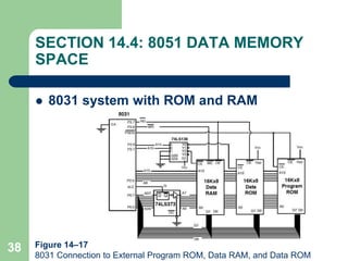
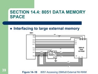
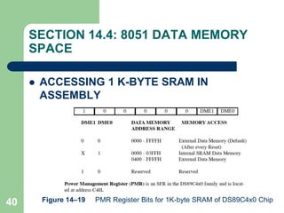
1
The 8051 Microcontroller and
Embedded Systems
CHAPTER 14
8051 INTERFACING
TO EXTERNAL
MEMORY
2
OBJECTIVES
 Contrast and compare various types of semiconductor memories in
terms of their capacity, organization, and access time
 Describe the relationship between the number of memory locations on
a chip, the number of data pins, and the chip capacity
 Define ROM memory and describe its use in 8051-based systems
 Contrast and compare PROM, EPROM, UV EPROM, EEPROM, flash
memory EPROM, and mask ROM memories
 Define RAM memory and describe its use in 8051-based systems
 Contrast and compare SRAM, NV-RAM, checksum byte, and DRAM
memories
 List the steps a CPU follows in memory address decoding
 Explain how to interface ROM with the 8031/51
 Explain how to use both on-chip and off-chip memory with the 8051
 Code 8051 Assembly programs accessing the 64K-byte data memory
space
3
SECTION 14.1: SEMICONDUCTOR
MEMORY
 Memory capacity
 The number of bits that a semiconductor
memory chip can store is called chip
capacity.
 It can be in units of Kbits (kilobits), Mbits
(megabits), and so on.
4
SECTION 14.1: SEMICONDUCTOR
MEMORY
 Memory organization
 Memory chips are organized into a
number of locations within the IC.
 Each location can hold 1 bit, 4 bits, 8 bits,
or even 16 bits, depending on how it is
designed internally.
5
SECTION 14.1: SEMICONDUCTOR
MEMORY
 Speed
 The speed of the memory chip
is commonly referred to as
its access time.
 The access time of memory chips
varies from a few nanoseconds to
hundreds of nanoseconds,
depending on the IC technology
used in the design and
abrication process.
Table 14–1 Powers of 2
6
SECTION 14.1: SEMICONDUCTOR
MEMORY
 ROM (read-only memory)
 ROM is a type of memory that does not
lose its contents when the power is
turned off.
 For this reason, ROM is also called
nonvolatile memory.
7
SECTION 14.1: SEMICONDUCTOR
MEMORY
 PROM (programmable ROM) and OTP
 PROM is programmed by blowing the
fuses.
 If the information burned into PROM is
wrong, that PROM must be discarded
since its internal fuses are blown
permanently.
8
SECTION 14.1: SEMICONDUCTOR
MEMORY
 EPROM (erasable programmable ROM)
and UV-EPROM
Figure 14–1 Pin Configurations for 27xx ROM Family
9
SECTION 14.1: SEMICONDUCTOR
MEMORY
Table 14–2 Some UV-EPROM Chips
10
SECTION 14.1: SEMICONDUCTOR
MEMORY
 EEPROM (electrically erasable
programmable ROM)
Table 14–3 Some EEPROM and Flash Chips
11
SECTION 14.1: SEMICONDUCTOR
MEMORY
 Flash memory EPROM
 flash memory can be programmed while it
is in its socket on the system board, it is
widely used to upgrade the BIOS ROM of
the PC.
 flash memory is semiconductor memory
with access time in the range of 100 ns
compared with disk access time in the
range of tens of milliseconds.
12
SECTION 14.1: SEMICONDUCTOR
MEMORY
 Mask ROM
 Mask ROM refers to a kind of ROM in
which the contents are programmed by
the IC manufacturer.
 Mask ROM is used when the needed
volume is high (hundreds of thousands)
and it is absolutely certain that the
contents will not change.
13
SECTION 14.1: SEMICONDUCTOR
MEMORY
 RAM (random access memory)
 RAM memory is called volatile memory
since cutting off the power to the IC
results in the loss of data.
14
SECTION 14.1: SEMICONDUCTOR
MEMORY
 SRAM (static RAM)
 Storage cells in static
RAM memory are
made of flip-flops
and therefore do
not require refreshing
in order to keep
their data.
 This is in contrast
to DRAM.
Figure 14–2
2Kx8 SRAM Pins
15
SECTION 14.1: SEMICONDUCTOR
MEMORY
Table 14–4 Some SRAM and NV-RAM Chips
16
SECTION 14.1: SEMICONDUCTOR
MEMORY
 NV-RAM (nonvolatile RAM)
 New type of nonvolatile RAM called NV-
RAM.
 Like other RAMS, it allows the CPU to
read and write to it, but when the power is
turned off the contents are not lost.
17
SECTION 14.1: SEMICONDUCTOR
MEMORY
 Checksum byte ROM
 checksum will detect any corruption of
the contents of ROM
18
SECTION 14.1: SEMICONDUCTOR
MEMORY
 DRAM (dynamic RAM)
uses a capacitor to
store each bit
 requires constant
refreshing due to
leakage
Figure 14–3 256Kx1 DRAM
19
SECTION 14.1: SEMICONDUCTOR
MEMORY
20
SECTION 14.1: SEMICONDUCTOR
MEMORY
 Packaging issue in DRAM
 In DRAM there is a problem of packing a
large number of cells into a single chip
with the normal number of pins assigned
to addresses
21
SECTION 14.1: SEMICONDUCTOR
MEMORY
 DRAM organization
22
SECTION 14.2: MEMORY ADDRESS
DECODING
 Simple logic gate address decoder
Figure 14–4 Logic Gate as Decoder
23
SECTION 14.2: MEMORY ADDRESS
DECODING
 Using the 74LS138 3-8 decoder
Figure 14–5
74LS138 Decoder
(Reprinted by permission of Texas Instruments,
Copyright Texas Instruments, 1988)
24
SECTION 14.2: MEMORY ADDRESS
DECODING
Figure 14–6 74LS138 as Decoder
25
SECTION 14.2: MEMORY ADDRESS
DECODING
 Using programmable logic as an address
decoder
 The advantage of these chips is that they can be
programmed for any combination of address
ranges, and so are much more versatile.
 PALs and GALS have 10 or more inputs (in
contrast to 6 in the 74138) means that they can
accommodate more address inputs.
26
SECTION 14.3: 8031/51 INTERFACING
WITH EXTERNAL ROM
 EA pin
 Connect the EA pin
to Vcc to indicate that
the program code is
stored in the mC's
on-chip ROM.
 To indicate that the program
code is stored in external ROM,
this pin must be connected
to GND.
Figure 14–7 8051 Pin Diagram
27
SECTION 14.3: 8031/51 INTERFACING
WITH EXTERNAL ROM
Figure 14–8
74LS373 D Latch
(Reprinted by permission of Texas Instruments,
Copyright Texas Instruments, 1988)
28
SECTION 14.3: 8031/51 INTERFACING
WITH EXTERNAL ROM
 P0 and P2 role in providing addresses
Figure 14–9 Address/Data Multiplexing
29
SECTION 14.3: 8031/51 INTERFACING
WITH EXTERNAL ROM
Figure 14–10 Data, Address, and Control Buses for the 8031
30
SECTION 14.3: 8031/51 INTERFACING
WITH EXTERNAL ROM
Figure 14–11 8031 Connection to External Program ROM
31
SECTION 14.3: 8031/51 INTERFACING
WITH EXTERNAL ROM
 PSEN
Figure 14–12 On-chip and Off-chip Program Code Access
32
SECTION 14.3: 8031/51 INTERFACING
WITH EXTERNAL ROM
 On-chip and off-chip code ROM
 In such a system we still have EA = Vcc,
meaning that upon reset the 8051
executes the on-chip program first; then,
when it reaches the end of the on-chip
ROM it switches to external ROM for the
rest of the program code.
33
SECTION 14.4: 8051 DATA MEMORY
SPACE
 Data memory space
Figure 14–13 8051 Connection to External Data ROM
34
SECTION 14.4: 8051 DATA MEMORY
SPACE
 External ROM for data
 For the ROM containing the program
code, PSEN is used to fetch the code.
 For the ROM containing data, the RD
signal is used to fetch the data.
35
SECTION 14.4: 8051 DATA MEMORY
SPACE
 MOVX instruction
Figure 14–14
8031 Connection to External Data ROM and External Program ROM
36
SECTION 14.4: 8051 DATA MEMORY
SPACE
 MOVX instruction for external RAM data
Figure 14–15 8051 Connection to External Data RAM
37
SECTION 14.4: 8051 DATA MEMORY
SPACE
 A single external ROM for code and data
Figure 14–16 A Single ROM for Both Program and Data
38
SECTION 14.4: 8051 DATA MEMORY
SPACE
 8031 system with ROM and RAM
Figure 14–17
8031 Connection to External Program ROM, Data RAM, and Data ROM
39
SECTION 14.4: 8051 DATA MEMORY
SPACE
 Interfacing to large external memory
Figure 14–18 8051 Accessing 256Kx8 External NV-RAM
40
SECTION 14.4: 8051 DATA MEMORY
SPACE
 ACCESSING 1 K-BYTE SRAM IN
ASSEMBLY
Figure 14–19 PMR Register Bits for 1K-byte SRAM of DS89C4x0 Chip
41
Next …
 Lecture Problems Textbook Chapter 11
– Answer as many questions as you can and
submit via MeL before the end of the lecture.

The 8051 Microcontroller and Embedded Systems

  • 1.
    1 The 8051 Microcontrollerand Embedded Systems CHAPTER 14 8051 INTERFACING TO EXTERNAL MEMORY
  • 2.
    2 OBJECTIVES  Contrast andcompare various types of semiconductor memories in terms of their capacity, organization, and access time  Describe the relationship between the number of memory locations on a chip, the number of data pins, and the chip capacity  Define ROM memory and describe its use in 8051-based systems  Contrast and compare PROM, EPROM, UV EPROM, EEPROM, flash memory EPROM, and mask ROM memories  Define RAM memory and describe its use in 8051-based systems  Contrast and compare SRAM, NV-RAM, checksum byte, and DRAM memories  List the steps a CPU follows in memory address decoding  Explain how to interface ROM with the 8031/51  Explain how to use both on-chip and off-chip memory with the 8051  Code 8051 Assembly programs accessing the 64K-byte data memory space
  • 3.
    3 SECTION 14.1: SEMICONDUCTOR MEMORY Memory capacity  The number of bits that a semiconductor memory chip can store is called chip capacity.  It can be in units of Kbits (kilobits), Mbits (megabits), and so on.
  • 4.
    4 SECTION 14.1: SEMICONDUCTOR MEMORY Memory organization  Memory chips are organized into a number of locations within the IC.  Each location can hold 1 bit, 4 bits, 8 bits, or even 16 bits, depending on how it is designed internally.
  • 5.
    5 SECTION 14.1: SEMICONDUCTOR MEMORY Speed  The speed of the memory chip is commonly referred to as its access time.  The access time of memory chips varies from a few nanoseconds to hundreds of nanoseconds, depending on the IC technology used in the design and abrication process. Table 14–1 Powers of 2
  • 6.
    6 SECTION 14.1: SEMICONDUCTOR MEMORY ROM (read-only memory)  ROM is a type of memory that does not lose its contents when the power is turned off.  For this reason, ROM is also called nonvolatile memory.
  • 7.
    7 SECTION 14.1: SEMICONDUCTOR MEMORY PROM (programmable ROM) and OTP  PROM is programmed by blowing the fuses.  If the information burned into PROM is wrong, that PROM must be discarded since its internal fuses are blown permanently.
  • 8.
    8 SECTION 14.1: SEMICONDUCTOR MEMORY EPROM (erasable programmable ROM) and UV-EPROM Figure 14–1 Pin Configurations for 27xx ROM Family
  • 9.
  • 10.
    10 SECTION 14.1: SEMICONDUCTOR MEMORY EEPROM (electrically erasable programmable ROM) Table 14–3 Some EEPROM and Flash Chips
  • 11.
    11 SECTION 14.1: SEMICONDUCTOR MEMORY Flash memory EPROM  flash memory can be programmed while it is in its socket on the system board, it is widely used to upgrade the BIOS ROM of the PC.  flash memory is semiconductor memory with access time in the range of 100 ns compared with disk access time in the range of tens of milliseconds.
  • 12.
    12 SECTION 14.1: SEMICONDUCTOR MEMORY Mask ROM  Mask ROM refers to a kind of ROM in which the contents are programmed by the IC manufacturer.  Mask ROM is used when the needed volume is high (hundreds of thousands) and it is absolutely certain that the contents will not change.
  • 13.
    13 SECTION 14.1: SEMICONDUCTOR MEMORY RAM (random access memory)  RAM memory is called volatile memory since cutting off the power to the IC results in the loss of data.
  • 14.
    14 SECTION 14.1: SEMICONDUCTOR MEMORY SRAM (static RAM)  Storage cells in static RAM memory are made of flip-flops and therefore do not require refreshing in order to keep their data.  This is in contrast to DRAM. Figure 14–2 2Kx8 SRAM Pins
  • 15.
    15 SECTION 14.1: SEMICONDUCTOR MEMORY Table14–4 Some SRAM and NV-RAM Chips
  • 16.
    16 SECTION 14.1: SEMICONDUCTOR MEMORY NV-RAM (nonvolatile RAM)  New type of nonvolatile RAM called NV- RAM.  Like other RAMS, it allows the CPU to read and write to it, but when the power is turned off the contents are not lost.
  • 17.
    17 SECTION 14.1: SEMICONDUCTOR MEMORY Checksum byte ROM  checksum will detect any corruption of the contents of ROM
  • 18.
    18 SECTION 14.1: SEMICONDUCTOR MEMORY DRAM (dynamic RAM) uses a capacitor to store each bit  requires constant refreshing due to leakage Figure 14–3 256Kx1 DRAM
  • 19.
  • 20.
    20 SECTION 14.1: SEMICONDUCTOR MEMORY Packaging issue in DRAM  In DRAM there is a problem of packing a large number of cells into a single chip with the normal number of pins assigned to addresses
  • 21.
  • 22.
    22 SECTION 14.2: MEMORYADDRESS DECODING  Simple logic gate address decoder Figure 14–4 Logic Gate as Decoder
  • 23.
    23 SECTION 14.2: MEMORYADDRESS DECODING  Using the 74LS138 3-8 decoder Figure 14–5 74LS138 Decoder (Reprinted by permission of Texas Instruments, Copyright Texas Instruments, 1988)
  • 24.
    24 SECTION 14.2: MEMORYADDRESS DECODING Figure 14–6 74LS138 as Decoder
  • 25.
    25 SECTION 14.2: MEMORYADDRESS DECODING  Using programmable logic as an address decoder  The advantage of these chips is that they can be programmed for any combination of address ranges, and so are much more versatile.  PALs and GALS have 10 or more inputs (in contrast to 6 in the 74138) means that they can accommodate more address inputs.
  • 26.
    26 SECTION 14.3: 8031/51INTERFACING WITH EXTERNAL ROM  EA pin  Connect the EA pin to Vcc to indicate that the program code is stored in the mC's on-chip ROM.  To indicate that the program code is stored in external ROM, this pin must be connected to GND. Figure 14–7 8051 Pin Diagram
  • 27.
    27 SECTION 14.3: 8031/51INTERFACING WITH EXTERNAL ROM Figure 14–8 74LS373 D Latch (Reprinted by permission of Texas Instruments, Copyright Texas Instruments, 1988)
  • 28.
    28 SECTION 14.3: 8031/51INTERFACING WITH EXTERNAL ROM  P0 and P2 role in providing addresses Figure 14–9 Address/Data Multiplexing
  • 29.
    29 SECTION 14.3: 8031/51INTERFACING WITH EXTERNAL ROM Figure 14–10 Data, Address, and Control Buses for the 8031
  • 30.
    30 SECTION 14.3: 8031/51INTERFACING WITH EXTERNAL ROM Figure 14–11 8031 Connection to External Program ROM
  • 31.
    31 SECTION 14.3: 8031/51INTERFACING WITH EXTERNAL ROM  PSEN Figure 14–12 On-chip and Off-chip Program Code Access
  • 32.
    32 SECTION 14.3: 8031/51INTERFACING WITH EXTERNAL ROM  On-chip and off-chip code ROM  In such a system we still have EA = Vcc, meaning that upon reset the 8051 executes the on-chip program first; then, when it reaches the end of the on-chip ROM it switches to external ROM for the rest of the program code.
  • 33.
    33 SECTION 14.4: 8051DATA MEMORY SPACE  Data memory space Figure 14–13 8051 Connection to External Data ROM
  • 34.
    34 SECTION 14.4: 8051DATA MEMORY SPACE  External ROM for data  For the ROM containing the program code, PSEN is used to fetch the code.  For the ROM containing data, the RD signal is used to fetch the data.
  • 35.
    35 SECTION 14.4: 8051DATA MEMORY SPACE  MOVX instruction Figure 14–14 8031 Connection to External Data ROM and External Program ROM
  • 36.
    36 SECTION 14.4: 8051DATA MEMORY SPACE  MOVX instruction for external RAM data Figure 14–15 8051 Connection to External Data RAM
  • 37.
    37 SECTION 14.4: 8051DATA MEMORY SPACE  A single external ROM for code and data Figure 14–16 A Single ROM for Both Program and Data
  • 38.
    38 SECTION 14.4: 8051DATA MEMORY SPACE  8031 system with ROM and RAM Figure 14–17 8031 Connection to External Program ROM, Data RAM, and Data ROM
  • 39.
    39 SECTION 14.4: 8051DATA MEMORY SPACE  Interfacing to large external memory Figure 14–18 8051 Accessing 256Kx8 External NV-RAM
  • 40.
    40 SECTION 14.4: 8051DATA MEMORY SPACE  ACCESSING 1 K-BYTE SRAM IN ASSEMBLY Figure 14–19 PMR Register Bits for 1K-byte SRAM of DS89C4x0 Chip
  • 41.
    41 Next …  LectureProblems Textbook Chapter 11 – Answer as many questions as you can and submit via MeL before the end of the lecture.