Downloaded 39 times
![AT89S52
Baud Rate Generator
Timer 2 is selected as the baud rate generator by setting
TCLK and/or RCLK in T2CON (Table 2). Note that the
baud rates for transmit and receive can be different if Timer
2 is used for the receiver or transmitter and Timer 1 is used
for the other function. Setting RCLK and/or TCLK puts
Timer 2 into its baud rate generator mode, as shown in Figure 8.
The baud rate generator mode is similar to the auto-reload
mode, in that a rollover in TH2 causes the Timer 2 registers
to be reloaded with the 16-bit value in registers RCAP2H
and RCAP2L, which are preset by software.
The baud rates in Modes 1 and 3 are determined by Timer
2’s overflow rate according to the following equation.
Timer 2 Overflow Rate
Modes 1 and 3 Baud Rates = ----------------------------------------------------------16
The Timer can be configured for either timer or counter
operation. In most applications, it is configured for timer
operation (CP/T2 = 0). The timer operation is different for
Timer 2 when it is used as a baud rate generator. Normally,
as a timer, it increments every machine cycle (at 1/12 the
oscillator frequency). As a baud rate generator, however, it
increments every state time (at 1/2 the oscillator frequency). The baud rate formula is given below.
Modes 1 and 3
Oscillator Frequency
-------------------------------------- = ------------------------------------------------------------------------------------Baud Rate
32 x [65536-RCAP2H,RCAP2L)]
where (RCAP2H, RCAP2L) is the content of RCAP2H and
RCAP2L taken as a 16-bit unsigned integer.
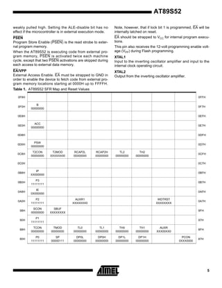
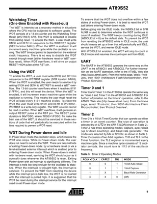
Timer 2 as a baud rate generator is shown in Figure 8. This
figure is valid only if RCLK or TCLK = 1 in T2CON. Note
that a rollover in TH2 does not set TF2 and will not generate an interrupt. Note too, that if EXEN2 is set, a 1-to-0
transition in T2EX will set EXF2 but will not cause a reload
from (RCAP2H, RCAP2L) to (TH2, TL2). Thus, when Timer
2 is in use as a baud rate generator, T2EX can be used as
an extra external interrupt.
Note that when Timer 2 is running (TR2 = 1) as a timer in
the baud rate generator mode, TH2 or TL2 should not be
read from or written to. Under these conditions, the Timer is
incremented every state time, and the results of a read or
write may not be accurate. The RCAP2 registers may be
read but should not be written to, because a write might
overlap a reload and cause write and/or reload errors. The
timer should be turned off (clear TR2) before accessing the
Timer 2 or RCAP2 registers.
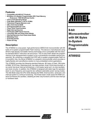
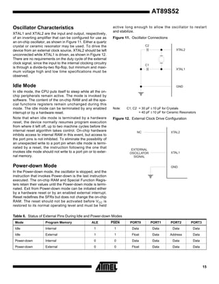
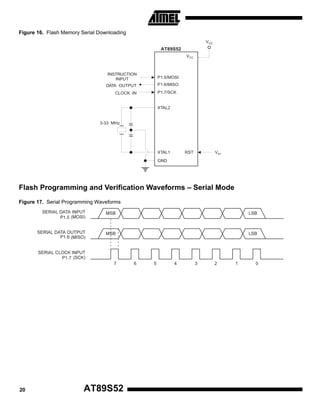
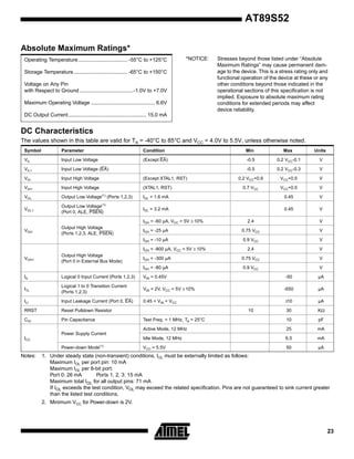
Figure 9. Timer 2 in Clock-Out Mode
OSC
TL2
(8-BITS)
÷2
TH2
(8-BITS)
TR2
RCAP2L RCAP2H
C/T2 BIT
P1.0
(T2)
÷2
T2OE (T2MOD.1)
TRANSITION
DETECTOR
P1.1
(T2EX)
EXF2
TIMER 2
INTERRUPT
EXEN2
13](https://image.slidesharecdn.com/at89s52-140118083458-phpapp01/85/At89s52-13-320.jpg)
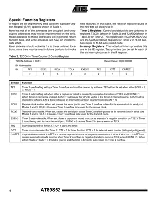
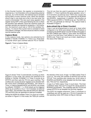
![Programmable Clock Out
A 50% duty cycle clock can be programmed to come out on
P1.0, as shown in Figure 9. This pin, besides being a regular I/O pin, has two alternate functions. It can be programmed to input the external clock for Timer/Counter 2 or
to output a 50% duty cycle clock ranging from 61 Hz to 4
MHz at a 16 MHz operating frequency.
To configure the Timer/Counter 2 as a clock generator, bit
C/T2 (T2CON.1) must be cleared and bit T2OE (T2MOD.1)
must be set. Bit TR2 (T2CON.2) starts and stops the timer.
The clock-out frequency depends on the oscillator frequency and the reload value of Timer 2 capture registers
(RCAP2H, RCAP2L), as shown in the following equation.
Table 5. Interrupt Enable (IE) Register
(MSB)
EA
(LSB)
–
ET2
ES
ET1
EX1
ET0
EX0
Enable Bit = 1 enables the interrupt.
Enable Bit = 0 disables the interrupt.
In the clock-out mode, Timer 2 roll-overs will not generate
an interrupt. This behavior is similar to when Timer 2 is
used as a baud-rate generator. It is possible to use Timer 2
as a baud-rate generator and a clock generator simultaneously. Note, however, that the baud-rate and clock-out
frequencies cannot be determined independently from one
another since they both use RCAP2H and RCAP2L.
Function
EA
IE.7
Disables all interrupts. If EA = 0,
no interrupt is acknowledged. If
EA = 1, each interrupt source is
individually enabled or disabled
by setting or clearing its enable
bit.
–
IE.6
Reserved.
IE.5
Timer 2 interrupt enable bit.
ES
IE.4
Serial Port interrupt enable bit.
ET1
IE.3
Timer 1 interrupt enable bit.
EX1
IE.2
External interrupt 1 enable bit.
ET0
IE.1
Timer 0 interrupt enable bit.
EX0
IE.0
External interrupt 0 enable bit.
User software should never write 1s to unimplemented bits,
because they may be used in future AT89 products.
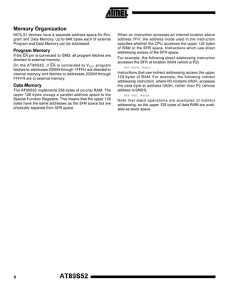
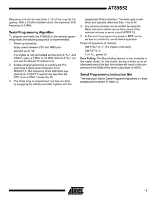
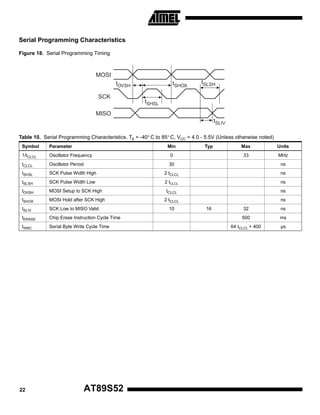
Interrupts
The AT89S52 has a total of six interrupt vectors: two external interrupts (INT0 and INT1), three timer interrupts (Timers 0, 1, and 2), and the serial port interrupt. These
interrupts are all shown in Figure 10.
Each of these interrupt sources can be individually enabled
or disabled by setting or clearing a bit in Special Function
Register IE. IE also contains a global disable bit, EA, which
disables all interrupts at once.
Note that Table 5 shows that bit position IE.6 is unimplemented. In the AT89S52, bit position IE.5 is also unimplemented. User software should not write 1s to these bit
positions, since they may be used in future AT89 products.
Timer 2 interrupt is generated by the logical OR of bits TF2
and EXF2 in register T2CON. Neither of these flags is
cleared by hardware when the service routine is vectored
to. In fact, the service routine may have to determine
whether it was TF2 or EXF2 that generated the interrupt,
and that bit will have to be cleared in software.
The Timer 0 and Timer 1 flags, TF0 and TF1, are set at
S5P2 of the cycle in which the timers overflow. The values
are then polled by the circuitry in the next cycle. However,
the Timer 2 flag, TF2, is set at S2P2 and is polled in the
same cycle in which the timer overflows.
14
Position
ET2
Oscillator Frequency
Clock-Out Frequency = -----------------------------------------------------------------------------------4 x [65536-(RCAP2H,RCAP2L)]
Symbol
AT89S52
Figure 10. Interrupt Sources
0
INT0
IE0
1
TF0
0
INT1
IE1
1
TF1
TI
RI
TF2
EXF2](https://image.slidesharecdn.com/at89s52-140118083458-phpapp01/85/At89s52-14-320.jpg)

The AT89S52 is a low-power, high-performance CMOS 8-bit microcontroller with 8KB of in-system programmable (ISP) flash memory, compatible with MCS-51 products. It features a wide range of functionalities including 32 I/O lines, two data pointers, three 16-bit timers, and various power-saving modes, making it suitable for embedded control applications. The device uses Atmel's high-density non-volatile memory technology and allows for reprogramming in-system or through conventional programmers.


