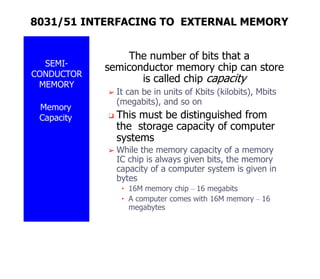
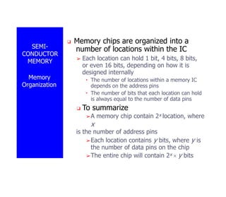
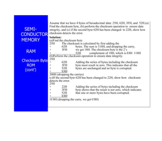
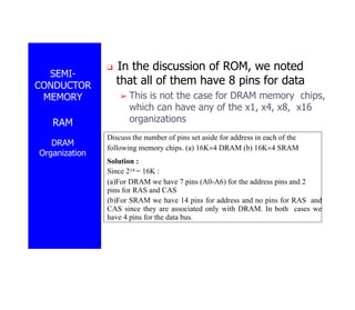
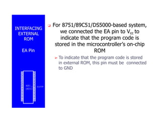
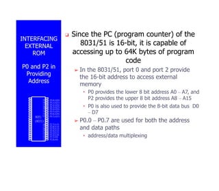
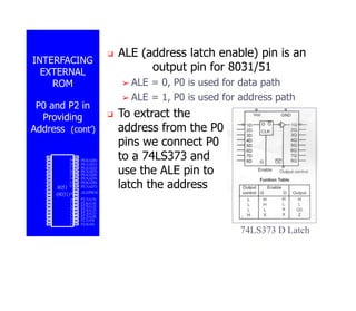
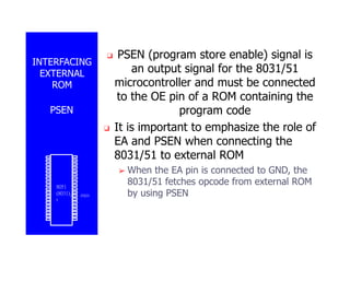
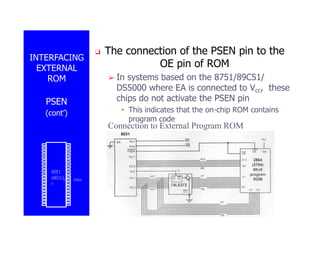
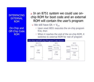
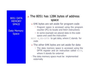
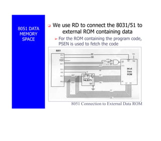
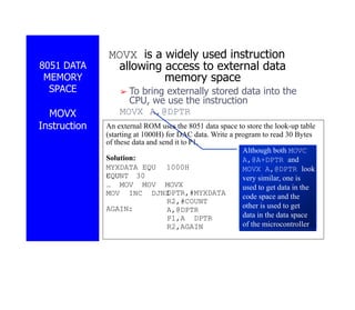
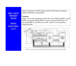
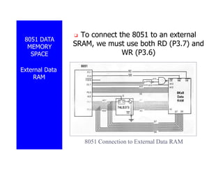
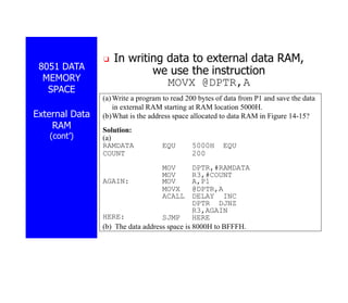
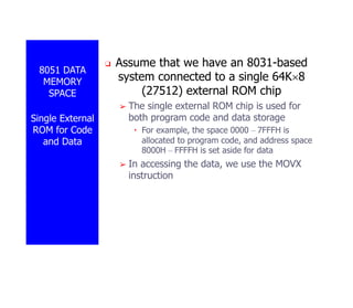
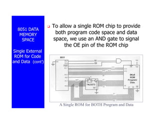
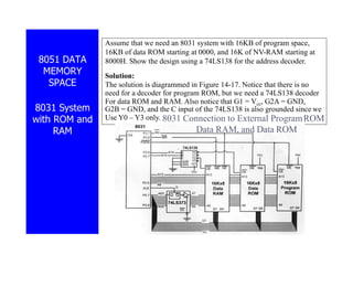
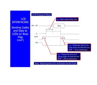
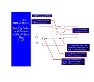
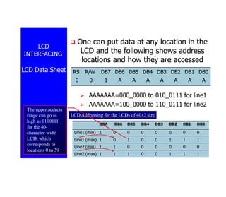
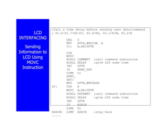
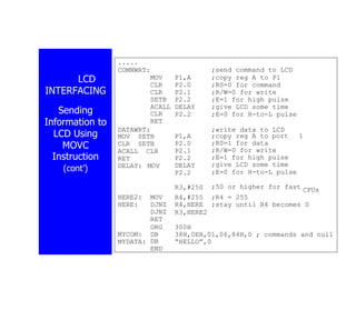
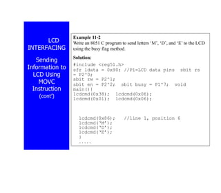
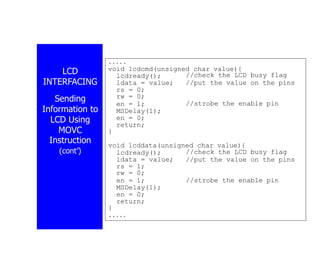
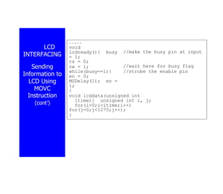
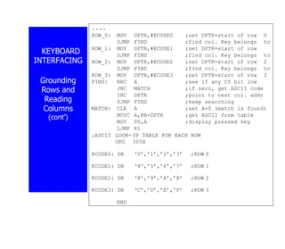
2. Teacher: Liu Zhongguo
Teaching material: Chen Guiyou. Single Microcomputer
Principles and Interface Technology (2nd Edition), Higher
Education Press, 2017
Website of Shanda Curriculum Center "Microcomputer
Principles and Microcontroller Interface Technology" :
http://course.sdu.edu.cn/G2S/Template/View.aspx?action
=view&courseType=0&courseId=5819
Hongjing Technology http://www.gxwmcu.com/
Reference Books:
STC15series MCU Data Sheet.2015.10
STC15W4K32S4 series MCU Data Sheet.2015.2
2
3. SEMI-
CONDUCTOR
MEMORY
Memory
Capacity
The number of bits that a
semiconductor memory chip can store
is called chip capacity
➢ It can be in units of Kbits (kilobits), Mbits
(megabits), and so on
❑ This must be distinguished from
the storage capacity of computer
systems
➢ While the memory capacity of a memory
IC chip is always given bits, the memory
capacity of a computer system is given in
bytes
▪ 16M memory chip – 16 megabits
▪ A computer comes with 16M memory – 16
megabytes
8031/51 INTERFACING TO EXTERNAL MEMORY
4. SEMI-
CONDUCTOR
MEMORY
Memory
Organization
❑ Memory chips are organized into a
number of locations within the IC
➢ Each location can hold 1 bit, 4 bits, 8 bits,
or even 16 bits, depending on how it is
designed internally
▪ The number of locations within a memory IC
depends on the address pins
▪ The number of bits that each location can hold
is always equal to the number of data pins
❑ To summarize
➢A memory chip contain 2x location, where
x
is the number of address pins
➢Each location contains y bits, where y is
the number of data pins on the chip
➢The entire chip will contain 2x y bits
5. SEMI-
CONDUCTOR
MEMORY
Speed
❑ One of the most important
characteristics of a memory chip is the
speed at which its data can be
accessed
➢ To access the data, the address is
presented to the address pins, the READ pin
is activated, and after a certain amount
of time has elapsed, the data shows up at the
data pins
➢ The shorter this elapsed time, the better,
and consequently, the more expensive the
memory chip
➢ The speed of the memory chip is commonly
referred to as its access time
6. SEMI-
CONDUCTOR
MEMORY
Speed
(cont’)
Example
A given memory chip has 12 address pins and 4 data pins. Find:
(a) The organization, and (b) the capacity.
Solution:
(a)This memory chip has 4096 locations (212 = 4096), and each
location can hold 4 bits of data. This gives an
organization of 4096 4, often represented as 4K 4.
(b)The capacity is equal to 16K bits since there is a total of 4K
locations and each location can hold 4 bits of data.
Example
A 512K memory chip has 8 pins for data. Find:
(a) The organization, and (b) the number of
address pins for this memory chip.
Solution:
(a)A memory chip with 8 data pins means that each location
within the chip can hold 8 bits of data. To find the number of
locations within this memory chip, divide the capacity by the
number of data pins. 512K/8 = 64K; therefore, the organization
for this memory chip is 64K 8
(b)The chip has 16 address lines since 216 = 64K
7. SEMI-
CONDUCTOR
MEMORY
ROM
(Read-only
Memory)
❑ ROM is a type of memory that does not
lose its contents when the power is
turned off
➢ ROM is also called nonvolatile memory
❑ There are different types of read-
only memory
➢ PROM
➢ EPROM
➢ EEPROM
➢ Flash EPROM
➢ Mask ROM
8. SEMI-
CONDUCTOR
MEMORY
ROM
PROM
(Programmable
ROM)
❑ PROM refers to the kind of ROM that
the user can burn information into
➢ PROM is a user-programmable memory
➢ For every bit of the PROM, there exists a
fuse
❑ If the information burned into PROM
is wrong, that PROM must be
discarded since its internal fuses
are blown permanently
➢ PROM is also referred to as OTP (one-time
programmable)
➢ Programming ROM, also called burning
ROM, requires special equipment called a
ROM burner or ROM programmer
9. SEMI-
CONDUCTOR
MEMORY
ROM
EPROM (Erasable
Programmable
ROM)
❑ EPROM was invented to allow making
changes in the contents of PROM after
it is burned
➢ In EPROM, one can program the memory
chip and erase it thousands of times
❑ A widely used EPROM is called UV-
EPROM
➢ UV stands for ultra-violet
➢ The only problem with UV-EPROM is that
erasing its contents can take up to 20
minutes
➢ All UV-EPROM chips have a window that is
used to shine ultraviolet (UV) radiation to
erase its contents
10. SEMI-
CONDUCTOR
MEMORY
ROM
EPROM (Erasable
Programmable
ROM)
(cont’)
❑ To program a UV-EPROM chip, the
following steps must be taken:
➢ Its contents must be erased
▪ To erase a chip, it is removed from its socket on
the system board and placed in EPROM erasure
equipment to expose it to UV radiation for 15-20
minutes
➢ Program the chip
▪ To program a UV-EPROM chip, place it in the
ROM burner
▪ To burn code or data into EPROM, the ROM
burner uses 12.5 volts, Vpp in the UV-EPROM
data sheet or higher, depending on the EPROM
type
▪ Place the chip back into its system board socket
11. SEMI-
CONDUCTOR
MEMORY
ROM
EPROM (Erasable
Programmable
ROM)
(cont’)
❑ There is an EPROM programmer
(burner), and there is also separate
EPROM erasure equipment
❑ The major disadvantage of UV-EPROM,
is that it cannot be programmed while
in the system board
❑ Notice the pattern of the IC numbers
Ex. 27128-25 refers to UV-EPROM that has a capacity of
128K bits and access time of 250 nanoseconds
➢ 27xx always refers to UV-EPROM chips
For ROM chip 27128, find the number of data and address pins.
Solution:
The 27128 has a capacity of 128K bits. It has 16K 8
organization (all ROMs have 8 data pins), which indicates that
there are 8 pins for data, and 14 pins for address (214 = 16K)
12. SEMI-
CONDUCTOR
MEMORY
ROM
EEPROM
(Electrically
Erasable
Programmable
ROM)
❑ EEPROM has several advantage over
EPROM
➢ Its method of erasure is electrical and
therefore instant, as opposed to the 20-
minute erasure time required for UV-
EPROM
➢ One can select which byte to be erased, in
contrast to UV-EPROM, in which the entire
contents of ROM are erased
➢ One can program and erase its contents
while it is still in the system board
▪ EEPROM does not require an external erasure
and programming device
▪ The designer incorporate into the system board
the circuitry to program the EEPROM
13. SEMI-
CONDUCTOR
MEMORY
ROM
Flash Memory
EPROM
❑ Flash EPROM has become a popular
user-programmable memory chip since
the early 1990s
➢ The process of erasure of the entire
contents takes less than a second, or might
say in a flash
▪ The erasure method is electrical
▪ It is commonly called flash memory
➢ The major difference between EEPROM and
flash memory is
▪ Flash memory’s contents are erased, then the
entire device is erased
– There are some flash memories are recently made
so that the erasure can be done block by block
▪ One can erase a desired section or byte on
EEPROM
14. SEMI-
CONDUCTOR
MEMORY
ROM
Flash Memory
EPROM
(cont’)
❑ It is believed that flash memory will
replace part of the hard disk as a mass
storage medium
➢ The flash memory can be programmed
while it is in its socket on the system board
▪ Widely used as a way to upgrade PC BIOS ROM
➢ Flash memory is semiconductor memory
with access time in the range of 100 ns
compared with disk access time in the
range of tens of milliseconds
➢ Flash memory’s program/erase cycles must
become infinite, like hard disks
▪ Program/erase cycle refers to the number of
times that a chip can be erased and
programmed before it becomes unusable
▪ The program/erase cycle is 100,000 for flash
and EEPROM, 1000 for UV-EPROM
15. SEMI-
CONDUCTOR
MEMORY
ROM
Mask ROM
❑ Mask ROM refers to a kind of ROM in
which the contents are programmed by
the IC manufacturer, not user-
programmable
➢ The terminology mask is used in IC
fabrication
➢ Since the process is costly, mask ROM is
used when the needed volume is high and it
is absolutely certain that the contents will
not change
➢ The main advantage of mask ROM is its cost,
since it is significantly cheaper than other
kinds of ROM, but if an error in the
data/code is found, the entire batch must be
thrown away
16. SEMI-
CONDUCTOR
MEMORY
RAM (Random
Access
Memory)
❑ RAM memory is called volatile
memory since cutting off the power
to the IC will result in the loss of data
➢ Sometimes RAM is also referred to as
RAWM (read and write memory), in
contrast to ROM, which cannot be written
to
❑ There are three types of RAM
➢ Static RAM (SRAM)
➢ NV-RAM (nonvolatile RAM)
➢ Dynamic RAM (DRAM)
17. SEMI-
CONDUCTOR
MEMORY
RAM
SRAM (Static
RAM)
❑ Storage cells in static RAM memory are
made of flip-flops and therefore do not
require refreshing in order to keep their
data
❑ The problem with the use of flip-flops
for storage cells is that each cell require
at least 6 transistors to build, and the
cell holds only 1 bit of data
➢ In recent years, the cells have been made of
4 transistors, which still is too many
➢ The use of 4-transistor cells plus the use of
CMOS technology has given birth to a high-
capacity SRAM, but its capacity is far below
DRAM
18. SEMI-
CONDUCTOR
MEMORY
RAM
NV-RAM
(Nonvolatile RAM)
❑ NV-RAM combines the best of RAM and
ROM
➢ The read and write ability of RAM, plus the
nonvolatility of ROM
❑ NV-RAM chip internally is made of
the following components
➢ It uses extremely power-efficient SRAM
cells built out of CMOS
➢ It uses an internal lithium battery as a
backup energy source
➢ It uses an intelligent control circuitry
▪ The main job of this control circuitry is to
monitor the Vcc pin constantly to detect loss of
the external power supply
19. SEMI-
CONDUCTOR
MEMORY
RAM
Checksum Byte
ROM
❑ To ensure the integrity of the ROM
contents, every system must perform
the checksum calculation
➢ The process of checksum will detect any
corruption of the contents of ROM
➢ The checksum process uses what is called
a checksum byte
▪ The checksum byte is an extra byte that is
tagged to the end of series of bytes of data
20. SEMI-
CONDUCTOR
MEMORY
RAM
Checksum Byte
ROM
(cont’)
❑ To calculate the checksum byte of a
series of bytes of data
➢ Add the bytes together and drop the carries
➢ Take the 2’s complement of the total sum,
and that is the checksum byte, which
becomes the last byte of the series
❑ To perform the checksum operation,
add all the bytes, including the
checksum byte
➢ The result must be zero
➢ If it is not zero, one or more bytes of data
have been changed
21. SEMI-
Assume that we have 4 bytes of hexadecimal data: 25H, 62H, 3FH, and 52H.(a)
Find the checksum byte, (b) perform the checksum operation to ensure data
integrity, and (c) if the second byte 62H has been changed to 22H, show how
checksum detects the error.
Solution:
(a)Find the checksum byte.
25H The checksum is calculated by first adding the
+ 62H bytes. The sum is 118H, and dropping the carry,
+ 3FH we get 18H. The checksum byte is the 2’s
+ 52H complement of 18H, which is E8H 118H
(b)Perform the checksum operation to ensure data integrity.
25H
+ 62H Adding the series of bytes including the checksum
+ 3FH byte must result in zero. This indicates that all the
+ 52H bytes are unchanged and no byte is corrupted.
+ E8H
200H (dropping the carries)
(c)If the second byte 62H has been changed to 22H, show how checksum
detects the error.
25H
+ 22H Adding the series of bytes including the checksum
+ 3FH byte shows that the result is not zero, which indicates
+ 52H that one or more bytes have been corrupted.
+ E8H
1C0H (dropping the carry, we get C0H)
CONDUCTOR
MEMORY
RAM
Checksum Byte
ROM
(cont’)
22. SEMI-
CONDUCTOR
MEMORY
RAM
DRAM (Dynamic
RAM)
❑ Dynamic RAM uses a capacitor to store
each bit
➢ It cuts down the number of transistors
needed to build the cell
➢ It requires constant refreshing due to
leakage
❑ The advantages and disadvantages
of DRAM memory
➢ The major advantages are high density
(capacity), cheaper cost per bit, and lower
power consumption per bit
➢ The disadvantages is that
▪ it must be refreshed periodically, due to the fact
that the capacitor cell loses its charge;
▪ While it is being refreshed, the data cannot be
accessed
23. SEMI-
CONDUCTOR
MEMORY
RAM
Packing Issue in
DRAM
❑ In DRAM there is a problem of packing
a large number of cells into a single
chip with the normal number of pins
assigned to addresses
➢ Using conventional method of data access,
large number of pins defeats the purpose
of high density and small packaging
▪ For example, a 64K-bit chip (64K1) must have
16 address lines and 1 data line, requiring 16 pins to
send in the address
➢ The method used is to split the address in
half and send in each half of the address
through the same pins, thereby requiring
fewer address pins
24. SEMI-
CONDUCTOR
MEMORY
RAM
Packing Issue in
DRAM
(cont’)
❑ Internally, the DRAM structure is
divided into a square of rows and
columns
❑ The first half of the address is called
the row and the second half is called
column
➢ The first half of the address is sent in
through the address pins, and by activating RAS
(row address strobe), the internal latches
inside DRAM grab the first half of the address
➢ After that, the second half of the address is
sent in through the same pins, and by
activating CAS (column address strobe), the
internal latches inside DRAM latch the
second half of the address
25. SEMI-
CONDUCTOR
MEMORY
RAM
DRAM
Organization
❑ In the discussion of ROM, we noted
that all of them have 8 pins for data
➢ This is not the case for DRAM memory chips,
which can have any of the x1, x4, x8, x16
organizations
Discuss the number of pins set aside for address in each of the
following memory chips. (a) 16K4 DRAM (b) 16K4 SRAM
Solution :
Since 214 = 16K :
(a)For DRAM we have 7 pins (A0-A6) for the address pins and 2
pins for RAS and CAS
(b)For SRAM we have 14 pins for address and no pins for RAS and
CAS since they are associated only with DRAM. In both cases we
have 4 pins for the data bus.
26. MEMORY
ADDRESS
DECODING
❑ The CPU provides the address of the
data desired, but it is the job of the
decoding circuitry to locate the selected
memory block
➢ Memory chips have one or more pins called
CS (chip select), which must be activated
for the memory’s contents to be accessed
➢ Sometimes the chip select is also referred to
as chip enable (CE)
27. MEMORY
ADDRESS
DECODING
(cont’)
❑ In connecting a memory chip to the
CPU, note the following points
➢ The data bus of the CPU is connected
directly to the data pins of the memory chip
➢ Control signals RD (read) and WR (memory
write) from the CPU are connected to the OE
(output enable) and WE (write enable) pins
of the memory chip
➢ In the case of the address buses, while the
lower bits of the address from the CPU go
directly to the memory chip address pins,
the upper ones are used to activate the CS
pin of the memory chip
28. MEMORY
ADDRESS
DECODING
(cont’)
❑ Normally memories are divided into
blocks and the output of the decoder
selects a given memory block
➢ Using simple logic gates
➢ Using the 74LS138
➢ Using programmable logics
29. MEMORY
ADDRESS
DECODING
Simple Logic
Gate Address
Decoder
❑ The simplest way of decoding circuitry
is the use of NAND or other gates
➢ The fact that the output of a NAND gate is
active low, and that the CS pin is also
active low makes them a perfect match
A15-A12 must be 0011 in
order to select the chip
This result in the assignment
of address 3000H to 3FFFH to
this memory chip
CS
RD WR
MEMR
MEMW
A0
A11
4K*8
D7 D0
D0
D7
A12
A13
A14
A15
A0
A11
30. MEMORY
ADDRESS
DECODING
Using 74LS138
3-8 Decoder
❑ This is one of the most widely used
address decoders
➢ The 3 inputs A, B, and C generate 8 active-
low outputs Y0 – Y7
▪ Each Y output is connected to CS of a memory
chip, allowing control of 8 memory blocks by a
single 74LS138
➢ In the 74LS138, where A, B, and C select
which output is activated, there are three
additional inputs, G2A, G2B, and G1
▪ G2A and G2B are both active low, and G1 is
active high
▪ If any one of the inputs G1, G2A, or G2B is not
connected to an address signal, they must be
activated permanently either by Vcc or ground,
depending on the activation level
31. MEMORY
ADDRESS
DECODING
Using 74LS138
3-8 Decoder
(cont’)
74LS138 Decoder
A
B
C
Enable
G2A G2B G1
Y0 Y1 Y2
Y4
Y3
Y5
Y6
Y7
FunctionTable
Inputs
Enable Select
G1 G2 C BA
X H X XX
Outputs
Y0 Y1 Y2 Y3 Y4 Y5 Y6 Y7
H H H H H H H H L X
X X X H H H H H H H H
H L L
L L L H H H H H H H H L L
L H
H L L
H L
H L L
H H
H L H
L L
H L H
L H
H L H
H L
H L H
H H
H L H H H H H H H H L
H H H H H H H H L H H
H H H H H H L H H H H
H H H H L H H H H H H
H H L H H H H H H
H H L
OE Vpp
A0
A11
4K*8
D7 D0
D0
D7
A0
A11
CE
MEMR
Vcc
A.Y0
Y1
B.Y2
C.Y4
G2A
Y3
G2B
Y5
Y6
G1
Y7
A12
A13
A14
A15
GND
Vcc
32. MEMORY
Looking at the design in Figure 14-6, find the address range for the
Following. (a) Y4, (b) Y2, and (c) Y7.
Solution :
(a)The address range for Y4 is calculated as follows.
A15 A14 A13 A12 A11 A10 A9 A8 A7 A6 A5 A4 A3 A2 A1 A0 0 1
0 0 0 0 0 0 0
0 0 0 0 0 0 0
0 1 0 0 1 1 1 1
1 1 1 1 1 1 1
1
The above shows that the range for Y4 is 4000H to 4FFFH. In Figure
14-6, notice that A15 must be 0 for the decoder to be activated. Y4 will
be selected when A14 A13 A12 = 100 (4 in binary). The remaining A11-
A0 will be 0 for the lowest address and 1 for the highest address.
(b)The address range for Y2 is 2000H to 2FFFH.
A15 A14 A13 A12 A11 A10 A9 A8 A7 A6 A5 A4 A3 A2 A1 A0 0 0
1 0 0 0 0 0 0
0 0 0 0 0 0 0
0 0 1 0 1 1 1 1
1 1 1 1 1 1 1
1
(c)The address range for Y7 is 7000H to 7FFFH.
A15 A14 A13 A12 A11 A10 A9 A8 A7 A6 A5 A4 A3 A2 A1 A0 0 1
1 1 0 0 0 0 0
0 0 0 0 0 0 0
0 1 1 1 1 1 1 1
1 1 1 1 1 1 1
1
ADDRESS
DECODING
Using 74LS138
3-8 Decoder
(cont’)
33. MEMORY
ADDRESS
DECODING
Using
Programmable
Logic
❑ Other widely used decoders are
programmable logic chips such as PAL
and GAL chips
➢ One disadvantage of these chips is that one
must have access to a PAL/GAL software
and burner, whereas the 74LS138 needs
neither of these
➢ The advantage of these chips is that they
are much more versatile since they can be
programmed for any combination of address
ranges
34. INTERFACING
EXTERNAL
ROM
❑ The 8031 chip is a ROMless version of
the 8051
➢ It is exactly like any member of the 8051
family as far as executing the instructions
and features are concerned, but it has no
on-chip ROM
➢ To make the 8031 execute 8051 code, it
must be connected to external ROM
memory containing the program code
❑ 8031 is ideal for many systems
where the on-chip ROM of 8051 is
not sufficient, since it allows the
program size to be as large as 64K
bytes
35. INTERFACING
EXTERNAL
ROM
EA Pin
❑ For 8751/89C51/DS5000-based system,
we connected the EA pin to Vcc to
indicate that the program code is
stored in the microcontroller’s on-chip
ROM
➢ To indicate that the program code is stored
in external ROM, this pin must be connected
to GND
-EA/VPP
8051 31
(8031)
36. INTERFACING
EXTERNAL
ROM
P0 and P2 in
Providing
Address
❑ Since the PC (program counter) of the
8031/51 is 16-bit, it is capable of
accessing up to 64K bytes of program
code
➢ In the 8031/51, port 0 and port 2 provide
the 16-bit address to access external
memory
▪ P0 provides the lower 8 bit address A0 – A7, and
P2 provides the upper 8 bit address A8 – A15
▪ P0 is also used to provide the 8-bit data bus D0
– D7
➢ P0.0 – P0.7 are used for both the address
and data paths
▪ address/data multiplexing
P0.0(AD0)
P0.1(AD1)
P0.2(AD2)
P0.3(AD3)
P0.4(AD4)
P0.5(AD5)
P0.6(AD6)
P0.7(AD7)
P2.7(A15)
P2.6(A14)
P2.5(A13)
P2.4(A12)
P2.3(A11)
P2.2(A10)
P2.1(A9)
P2.0(A8)
39
38
37
36
35
34
33
28
27
26
25
24
23
22
21
8051 32
(8031)
37. INTERFACING
EXTERNAL
ROM
P0 and P2 in
Providing
Address (cont’)
❑ ALE (address latch enable) pin is an
output pin for 8031/51
➢ ALE = 0, P0 is used for data path
➢ ALE = 1, P0 is used for address path
74LS373 D Latch
❑ To extract the
address from the P0
pins we connect P0
to a 74LS373 and
use the ALE pin to
latch the address
P0.0(AD0)
P0.1(AD1)
P0.2(AD2)
P0.3(AD3)
P0.4(AD4)
P0.5(AD5)
P0.6(AD6)
P0.7(AD7)
ALE/PROG
P2.7(A15)
P2.6(A14)
P2.5(A13)
P2.4(A12)
P2.3(A11)
P2.2(A10)
P2.1(A9)
P2.0(A8)
39
38
37
36
35
34
33
8051 32
(8031)30
28
27
26
25
24
23
22
21
38. INTERFACING
EXTERNAL
ROM
P0 and P2 in
Providing
Address (cont’)
❑ Normally ALE = 0, and P0 is used as a
data bus, sending data out or bringing
data in
❑ Whenever the 8031/51 wants to use P0
as an address bus, it puts the
addresses A0 – A7 on the P0 pins and
activates ALE = 1 Address/Data Multiplexing
P0.0(AD0)
P0.1(AD1)
P0.2(AD2)
P0.3(AD3)
P0.4(AD4)
P0.5(AD5)
P0.6(AD6)
P0.7(AD7)
ALE/PROG
P2.7(A15)
P2.6(A14)
P2.5(A13)
P2.4(A12)
P2.3(A11)
P2.2(A10)
P2.1(A9)
P2.0(A8)
39
38
37
36
35
34
33
8051 32
(8031)30
28
27
26
25
24
23
22
21
39. INTERFACING
EXTERNAL
ROM
PSEN
❑ PSEN (program store enable) signal is
an output signal for the 8031/51
microcontroller and must be connected
to the OE pin of a ROM containing the
program code
❑ It is important to emphasize the role of
EA and PSEN when connecting the
8031/51 to external ROM
➢ When the EA pin is connected to GND, the
8031/51 fetches opcode from external ROM
by using PSEN
-PSEN
8051
(8031)2
9
40. INTERFACING
EXTERNAL
ROM
PSEN
(cont’)
❑ The connection of the PSEN pin to the
OE pin of ROM
➢ In systems based on the 8751/89C51/
DS5000 where EA is connected to Vcc, these
chips do not activate the PSEN pin
▪ This indicates that the on-chip ROM contains
program code
Connection to External Program ROM
-PSEN
8051
(8031)2
9
41. INTERFACING
EXTERNAL
ROM
On-Chip and
Off-Chip Code
ROM
❑ In an 8751 system we could use on-
chip ROM for boot code and an external
ROM will contain the user’s program
➢ We still have EA = Vcc,
▪ Upon reset 8051 executes the on-chip program
first, then
▪ When it reaches the end of the on-chip ROM, it
switches to external ROM for rest of program
8031/51
EA = GND
Off
Chip
0000
FFFF
~ ~
8051
EA = Vcc
FFFF
Off
Chip
~ ~
On-chip
0000
0FFF
1000
FFFF
8052
EA = Vcc
0000
Off
Chip
~ ~
On-chip
1FFF
2000
On-chip and Off-chip Program Code Access
42. INTERFACING
Discuss the program ROM space allocation for each of the following
cases.
(a)EA = 0 for the 8751 (89C51) chip.
(b)EA = Vcc with both on-chip and off-chip ROM for the 8751.
(c)EA = Vcc with both on-chip and off-chip ROM for the 8752.
Solution:
(a)When EA = 0, the EA pin is strapped to GND, and all program
fetches are directed to external memory regardless of whether or not the
8751 has some on-chip ROM for program code. This external ROM can
be as high as 64K bytes with address space of 0000 – FFFFH. In this
case an 8751(89C51) is the same as the 8031 system.
(b)With the 8751 (89C51) system where EA=Vcc, it fetches the program
code of address 0000 – 0FFFH from on-chip ROM since it has 4K bytes
of on-chip program ROM and any fetches from addresses 1000H –
FFFFH are directed to external ROM.
(c)With the 8752 (89C52) system where EA=Vcc, it fetches the program
code of addresses 0000 – 1FFFH from on-chip ROM since it has 8K
bytes of on-chip program ROM and any fetches from addresses 2000H –
FFFFH are directed to external ROM
EXTERNAL
ROM
On-Chip and
Off-Chip Code
ROM
(cont’)
43. 8051 DATA
MEMORY
SPACE
Data Memory
Space
❑ The 8051 has 128K bytes of address
space
➢ 64K bytes are set aside for program code
▪ Program space is accessed using the program
counter (PC) to locate and fetch instructions
▪ In some example we placed data in the code
space and used the instruction
MOVC A,@A+DPTR to get data, where C stands for
code
➢ The other 64K bytes are set aside for data
▪ The data memory space is accessed using the
DPTR register and an instruction called MOVX,
where X stands for external
– The data memory space must be implemented
externally
44. 8051 DATA
MEMORY
SPACE
❑ We use RD to connect the 8031/51 to
external ROM containing data
➢ For the ROM containing the program code,
PSEN is used to fetch the code
External ROM for Data
8051 Connection to External Data ROM
45. 8051 DATA
MEMORY
SPACE
MOVX
Instruction
MOVX is a widely used instruction
allowing access to external data
memory space
➢ To bring externally stored data into the
CPU, we use the instruction
MOVX A,@DPTR
An external ROM uses the 8051 data space to store the look-up table
(starting at 1000H) for DAC data. Write a program to read 30 Bytes
of these data and send it to P1.
COUNT
AGAIN:
Solution:
MYXDATA EQU 1000H
EQU 30
… MOV MOV MOVX
MOV INC DJNZ
DPTR,#MYXDATA
R2,#COUNT
A,@DPTR
P1,A DPTR
R2,AGAIN
Although both MOVC
A,@A+DPTR and
MOVX A,@DPTR look
very similar, one is
used to get data in the
code space and the
other is used to get
data in the data space
of the microcontroller
46. 8051 DATA
MEMORY
SPACE
MOVX
Instruction
(cont’)
Show the design of an 8031-based system with 8K bytes of program
ROM and 8K bytes of data ROM.
Solution:
Figure 14-14 shows the design. Notice the role of PSEN and RD in each
ROM. For program ROM, PSEN is used to activate both OE and CE.
For data ROM, we use RD to active OE, while CE is activated by a
Simple decoder.
8031 Connection to External Data ROM and External Program ROM
48. 8051 DATA
MEMORY
SPACE
External Data
RAM
(cont’)
❑ In writing data to external data RAM,
we use the instruction
MOVX @DPTR,A
(a)Write a program to read 200 bytes of data from P1 and save the data
in external RAM starting at RAM location 5000H.
(b)What is the address space allocated to data RAM in Figure 14-15?
Solution:
(a)
RAMDATA
COUNT
AGAIN:
HERE:
EQU 5000H EQU
200
MOV DPTR,#RAMDATA
MOV R3,#COUNT
MOV A,P1
MOVX @DPTR,A
ACALL DELAY INC
DPTR DJNZ
R3,AGAIN
SJMP HERE
(b) The data address space is 8000H to BFFFH.
49. 8051 DATA
MEMORY
SPACE
Single External
ROM for Code
and Data
❑ Assume that we have an 8031-based
system connected to a single 64K8
(27512) external ROM chip
➢ The single external ROM chip is used for
both program code and data storage
▪ For example, the space 0000 – 7FFFH is
allocated to program code, and address space
8000H – FFFFH is set aside for data
➢ In accessing the data, we use the MOVX
instruction
50. 8051 DATA
MEMORY
SPACE
Single External
ROM for Code
and Data (cont’)
❑ To allow a single ROM chip to provide
both program code space and data
space, we use an AND gate to signal
the OE pin of the ROM chip
A Single ROM for BOTH Program and Data
51. 8051 DATA
MEMORY
SPACE
8031 System
with ROM and
RAM
Assume that we need an 8031 system with 16KB of program space,
16KB of data ROM starting at 0000, and 16K of NV-RAM starting at
8000H. Show the design using a 74LS138 for the address decoder.
Solution:
The solution is diagrammed in Figure 14-17. Notice that there is no
need for a decoder for program ROM, but we need a 74LS138 decoder
For data ROM and RAM. Also notice that G1 = Vcc, G2A = GND,
G2B = GND, and the C input of the 74LS138 is also grounded since we
Use Y0 – Y3 only. 8031 Connection to External ProgramROM
Data RAM, and Data ROM
52. 8051 DATA
MEMORY
SPACE
Interfacing to
Large External
Memory
❑ In some applications we need a large
amount of memory to store data
➢ The 8051 can support only 64K bytes of
external data memory since DPTR is 16-bit
❑ To solve this problem, we connect
A0 – A15 of the 8051 directly to the
external memory’s A0 – A15 pins,
and use some of the P1 pins to
access the 64K bytes blocks inside
the single 256K8 memory chip
54. 8051 DATA
MEMORY
SPACE
Interfacing to
Large External
Memory
(cont’)
In a certain application, we need 256K bytes of NV-RAM to store data
collected by an 8051 microcontroller. (a) Show the connection of an
8051 to a single 256K8 NV-RAM chip. (b) Show how various blocks
of this single chip are accessed
Solution:
(a)The 256K8 NV-RAM has 18 address pins (A0 – A17) and 8 data
lines. As shown in Figure 14-18, A0 – A15 go directly to the
memory chip while A16 and A17 are controlled by P1.0 and P1.1,
respectively. Also notice that chip select of external RAM is
connected to P1.2 of the 8051.
(b)The 256K bytes of memory are divided into four blocks, and each
block is accessed as follows :
Chip select A17 A16
P1.2 P1.1 P1.0 Block address space
0 0 0 00000H - 0FFFFH
0 0 1 10000H -1FFFFH
0 1 0 20000H -2FFFFH
0 1 1 30000H - 3FFFFH
1 x x External RAM disabled
….
55. 8051 DATA
MEMORY
SPACE
Interfacing to
Large External
Memory
(cont’)
….
For example, to access the 20000H – 2FFFFH address space we need
the following :
CLR
MOV
CLR
P1.2
DPTR,#0
P1.0
;enable external RAM
;start of 64K memory block
;A16 = 0
SETB P1.1 ;A17 = 1 for 20000H block
MOV A,SBUF ;get data from serial port
MOVX @DPTR,A
INC DPTR ;next location
...
56. INTERFACING
LCD TO 8051
LCD Operation
❑LCD is finding widespread use replacing LEDs
➢The declining prices of LCD
➢The ability to display numbers, characters, and
graphics
➢Incorporation of a refreshing controller into the
LCD, thereby relieving the CPU of the task of
refreshing the LCD
➢Ease of programming for characters and graphics
1
REAL-WORLD INTERFACING I LCD, ADC, AND SENSORS
59. LCD
INTERFACING
LCD Operation
❑ LCD is finding widespread use
replacing LEDs
➢ The declining prices of LCD
➢ The ability to display numbers, characters,
and graphics
➢ Incorporation of a refreshing controller into
the LCD, thereby relieving the CPU of the
task of refreshing the LCD
➢ Ease of programming for characters and
graphics
LCD AND KEYBOARD INTERFACING
60. LCD
INTERFACING
LCD Pin
Descriptions
Pin Descriptions for LCD
Descriptions
Ground
+5V power supply
Power supply to control contrast
RS=0 to select command register,
RS=1 to select data register
R/W=0 for write,
R/W=1 for read
Enable
The 8-bit data bus
The 8-bit data bus
The 8-bit data bus
The 8-bit data bus
The 8-bit data bus
The 8-bit data bus
The 8-bit data bus
The 8-bit data bus
Pin Symbol I/O
1 VSS --
2 VCC --
3 VEE --
4 RS I
5 R/W I
6 E I/O
7 DB0 I/O
8 DB1 I/O
9 DB2 I/O
10 DB3 I/O
11 DB4 I/O
12 DB5 I/O
13 DB6 I/O
14 DB7 I/O
used by the
LCD to latch
information
presented to
its data bus
-Send displayed
information or
instruction
command codes to
the LCD
-Read the contents
of the LCD’s
internal registers
61. LCD
INTERFACING
LCD Command
Codes
LCD Command Codes
Code (Hex) Command to LCD Instruction Register
1 Clear display screen
2 Return home
4 Decrement cursor (shift cursor to left)
6 Increment cursor (shift cursor to right)
5 Shift display right
7 Shift display left
8 Display off, cursor off
A Display off, cursor on
C Display on, cursor off
E Display on, cursor blinking
F Display on, cursor blinking
10 Shift cursor position to left
14 Shift cursor position to right
18 Shift the entire display to the left
1C Shift the entire display to the right
80 Force cursor to beginning to 1st line
C0 Force cursor to beginning to 2nd line
38 2 lines and 5x7 matrix
62. LCD
INTERFACING
Sending Data/
Commands to
LCDs w/ Time
Delay
To send any of the commands to the LCD, make pin RS=0. For data,
make RS=1. Then send a high-to-low pulse to the E pin to enable the
internal latch of the LCD. This is shown in the code below.
;calls a time delay before sending next data/command
;P1.0-P1.7 are connected to LCD data pins D0-D7
;P2.0 is connected to RS pin of LCD
;P2.1 is connected to R/W pin of LCD
;P2.2 is connected to E pin of LCD
ORG 0H
MOV A,#38H ;INIT. LCD 2 LINES, 5X7 MATRIX
ACALL COMNWRT ;call command subroutine
ACALL DELAY
MOV A,#0EH
;give LCD some time
;display on, cursor on
ACALL COMNWRT ;call command subroutine
ACALL DELAY
MOV A,#01
;give LCD some time
;clear LCD
ACALL COMNWRT ;call command subroutine
ACALL DELAY
MOV A,#06H
;give LCD some time
;shift cursor right
ACALL COMNWRT ;call command subroutine
ACALL DELAY
MOV A,#84H
;give LCD some time
;cursor at line 1, pos. 4
ACALL COMNWRT ;call command subroutine
ACALL DELAY ;give LCD some time
.....
P2.0
P2.1
P2.2
RS R/W E
8051
P1.0 D0
P1.7 D7
VCC
VEE
VSS
10k
POT
LCD
+5V
63. LCD
INTERFACING
Sending Data/
Commands to
LCDs w/ Time
Delay
(cont’)
.....
MOV A,#’N’
ACALL DATAWRT
ACALL DELAY
MOV A,#’O’
ACALL DATAWRT
AGAIN: SJMP AGAIN
COMNWRT:
MOV P1,A
CLR P2.0
CLR P2.1
SETB P2.2
ACALL DELAY
P2.2
CLR
RET
DATA
WRT:
MOV
SETB
CLR
P1,A
P2.0
P2.1
SETB P2.2
ACALL DELAY
DELAY:
HERE2:
HERE:
;display letter N
;call display subroutine
;give LCD some time
;display letter O
;call display subroutine
;stay here
;send command to LCD
;copy reg A to port 1
;RS=0 for command
;R/W=0 for write
;E=1 for high pulse
;give LCD some time
;E=0 for H-to-L pulse
;write data to LCD
;copy reg A to port 1
;RS=1 for data
;R/W=0 for write
;E=1 for high pulse
;give LCD some time
;E=0 for H-to-L pulse
;50 or higher for fast CPUs
;R4 = 255
;stay until R4 becomes 0
CLR P2.2
RET
MOV R3,#50
MOV R4,#255
DJNZ R4,HERE
DJNZ R3,HERE2
RET
P2.0
P2.1
RS R/W E
8051
P1.0 D0
P1.7 D7
VCC
VEE
VSS
10k
POT
LCD
+5V
END
P2.2
64. LCD
INTERFACING
Sending Data/
Commands to
LCDs w/ Time
Delay
(cont’)
;Check busy flag before sending data, command to LCD
;p1=data pin
;P2.0 connected to RS pin
;P2.1 connected to R/W pin
;P2.2 connected to E pin
ORG 0H
MOV A,#38H
ACALL COMMAND
MOV A,#0EH
ACALL COMMAND
MOV A,#01H
ACALL COMMAND
MOV A,#06H
ACALL COMMAND
MOV A,#86H
ACALL COMMAND
MOV A,#’N’
;init. LCD 2 lines ,5x7 matrix
;issue command
;LCD on, cursor on
;issue command
;clear LCD command
;issue command
;shift cursor right
;issue command
;cursor: line 1, pos. 6
;command subroutine
;display letter N
ACALL DATA_DISPLAY
MOV A,#’O’ ;display letter O
ACALL DATA_DISPLAY
HERE ;STAY HERE
HERE:SJMP
.....
P2.0
P2.1
P2.2
RS R/W E
8051
P1.0 D0
P1.7 D7
VCC
VEE
VSS
10k
POT
LCD
+5V
65. LCD
INTERFACING
Sending Codes
and Data to
LCDs w/ Busy
Flag
(cont’)
..... COMMAND:
ACALL READY
MOV P1,A
CLR P2.0
CLR P2.1
SETB P2.2
CLR P2.2
;is LCD ready?
;issue command code
;RS=0 for command
;R/W=0 to write to LCD
;E=1 for H-to-L pulse
;E=0,latch in
RET
DATA_DISPLAY:
ACALL READY ;is LCD ready?
;issue data
;RS=1 for data
;R/W =0 to write to LCD
;E=1 for H-to-L pulse
MOV P1,A
SETB P2.0
CLR P2.1
SETB P2.2
CLR P2.2 ;E=0,latch in
RET
READY:
SETB P1.7 ;make P1.7 input port
CLR P2.0 ;RS=0 access command reg
SETB P2.1 ;R/W=1 read command reg
;read command reg and check busy flag
BACK:SETB P2.2
CLR P2.2
JB P1.7,BACK
;E=1 for H-to-L pulse
;E=0 H-to-L pulse
;stay until busy flag=0
RET
END
To read the command register, we make R/W=1,
RS=0, and a H-to-L pulse for the E pin.
P2.0
P2.1
P2.2
RS R/W E
8051
P1.0 D0
P1.7 D7
VCC
VEE
VSS
10k
POT
LCD
+5V
If bit 7 (busy flag) is high, the LCD is busy
and no information should be issued to it.
66. LCD
INTERFACING
Sending Codes
and Data to
LCDs w/ Busy
Flag
(cont’)
LCD Timing for Read
E
R/W
RS
Data
tAS tAH
tD
tD = Data output delay time
tAS = Setup time prior to E
(going high) for both RS and
R/W = 140 ns (minimum)
tAH = Hold time after E has
come down for both RS and
R/W = 10 ns (minimum)
Note : Read requires an L-to-H pulse for the E pin
D0 – D7
67. LCD
INTERFACING
Sending Codes
and Data to
LCDs w/ Busy
Flag
(cont’)
LCD Timing for Write
E
R/W
RS
Data
tAS
tDSW
tPWH
tH
tAH
tPWH = Enable pulse width
= 450 ns (minimum)
tDSW = Data set up time
= 195 ns (minimum)
tH = Data hold time
= 10 ns (minimum)
tAS = Setup time prior to E
(going high) for both RS and
R/W = 140 ns (minimum)
tAH = Hold time after E has
come down for both RS and
R/W = 10 ns (minimum)
68. LCD
INTERFACING
LCD Data Sheet
❑ One can put data at any location in the
LCD and the following shows address
locations and how they are accessed
➢ AAAAAAA=000_0000 to 010_0111 for line1
➢ AAAAAAA=100_0000 to 110_0111 for line2
DB7 DB6 DB5 DB4 DB3 DB2 DB1 DB0
Line1 (min) 1 0 0 0 0 0 0 0
Line1 (max) 1 0 1 0 0 1 1 1
Line2 (min) 1 1 0 0 0 0 0 0
Line2 (max) 1 1 1 0 0 1 1 1
LCD Addressing for the LCDs of 402 size
RS R/W DB7 DB6 DB5 DB4 DB3 DB2 DB1 DB0
0 0 1 A A A A A A A
The upper address
range can go as
high as 0100111
for the 40-
character-wide
LCD, which
corresponds to
locations 0 to 39
69. LCD
INTERFACING
Sending
Information to
LCD Using
MOVC
Instruction
;Call a time delay before sending next data/command
; P1.0-P1.7=D0-D7, P2.0=RS, P2.1=R/W, P2.2=E
ORG
MOV
C1:
CLR
MOVC
0
DPTR,#MYCOM A
A,@A+DPTR
ACALL COMNWRT ;call command subroutine
ACALL DELAY ;give LCD some time
INC DPTR
JZ SEND_DAT
SJMP
SEND_
DAT:
C1
MOV DPTR,#MYDATA
D1: CLR A
MOVC A,@A+DPTR
ACALL DATAWRT ;call command subroutine
ACALL DELAY ;give LCD some time
INC DPTR
JZ AGAIN
SJMP D1
AGAIN: SJMP AGAIN ;stay here
.....
70. LCD
INTERFACING
Sending
Information to
LCD Using
MOVC
Instruction
(cont’)
;copy reg A to port
.....
COMNWRT: ;send command to LCD
MOV P1,A ;copy reg A to P1
CLR P2.0 ;RS=0 for command
CLR P2.1 ;R/W=0 for write
SETB P2.2 ;E=1 for high pulse
ACALL DELAY ;give LCD some time
CLR
RET
P2.2 ;E=0 for H-to-L pulse
DATAWRT:
MOV SETB
CLR SETB
ACALL CLR
RET
DELAY: MOV
P1,A
P2.0
P2.1
P2.2
DELAY
P2.2
R3,#250
;write data to LCD
1
;RS=1 for data
;R/W=0 for write
;E=1 for high pulse
;give LCD some time
;E=0 for H-to-L pulse
;50 or higher for fast CPUs
HERE2:
HERE:
MOV
DJNZ
R4,#255
R4,HERE
;R4 = 255
;stay until R4 becomes 0
DJNZ
RET
R3,HERE2
MYCOM:
ORG
DB
300H
38H,0EH,01,06,84H,0 ; commands and null
MYDATA: DB
END
“HELLO”,0
71. LCD
INTERFACING
Sending
Information to
LCD Using
MOVC
Instruction
(cont’)
Example 11-2
Write an 8051 C program to send letters ‘M’, ‘D’, and ‘E’ to the LCD
using the busy flag method.
Solution:
#include <reg51.h>
sfr ldata = 0x90; //P1=LCD data pins sbit rs
= P2^0;
sbit rw = P2^1;
sbit en = P2^2; sbit busy = P1^7; void
main(){
lcdcmd(0x38); lcdcmd(0x0E);
lcdcmd(0x01); lcdcmd(0x06);
lcdcmd(0x86); //line 1, position 6
lcdcmd(‘M’);
lcdcmd(‘D’);
lcdcmd(‘E’);
}
.....
72. LCD
INTERFACING
Sending
Information to
LCD Using
MOVC
Instruction
(cont’)
.....
void lcdcmd(unsigned char value){
//check the LCD busy flag
//put the value on the pins
//strobe the enable pin
lcdready();
ldata = value;
rs = 0;
rw = 0;
en = 1;
MSDelay(1);
en = 0;
return;
}
void lcddata(unsigned char value){
//check the LCD busy flag
//put the value on the pins
//strobe the enable pin
lcdready();
ldata = value;
rs = 1;
rw = 0;
en = 1;
MSDelay(1);
en = 0;
return;
}
.....
73. LCD
INTERFACING
Sending
Information to
LCD Using
MOVC
Instruction
(cont’)
//make the busy pin at input
//wait here for busy flag
//strobe the enable pin
.....
void
lcdready(){ busy
= 1;
rs = 0;
rw = 1;
while(busy==1){
en = 0;
MSDelay(1); en =
1;
}
void lcddata(unsigned int
itime){ unsigned int i, j;
for(i=0;i<itime;i++)
for(j=0;j<1275;j++);
}
74. KEYBOARD
INTERFACING
❑ Keyboards are organized in a matrix of
rows and columns
➢ The CPU accesses both rows and columns
through ports
▪ Therefore, with two 8-bit ports, an 8 x 8 matrix
of keys can be connected to a microprocessor
➢ When a key is pressed, a row and a
column make a contact
▪ Otherwise, there is no connection between
rows and columns
❑ In IBM PC keyboards, a single
microcontroller takes care of
hardware and software interfacing
75. KEYBOARD
INTERFACING
Scanning and
Identifying the
Key
❑ A 4x4 matrix connected to two ports
➢ The rows are connected to an output port
and the columns are connected to an
input port
Matrix Keyboard Connection to ports
B
3
7
F
A
2
6
E
9
1
5
D
8
0
4
C
D3 D2 D1 D0
D0
D1
D2
D3
Port 1
(Out) Port 2
(In)
Vcc
If no key has
been pressed,
reading the
input port will
yield 1s for all
columns since
they are all
connected to
high (Vcc)
If all the rows are
grounded and a key
is pressed, one of
the columns will
have 0 since the key
pressed provides the
path to ground
76. KEYBOARD
INTERFACING
Grounding
Rows and
Reading
Columns
❑ It is the function of the microcontroller
to scan the keyboard continuously to
detect and identify the key pressed
❑ To detect a pressed key, the
microcontroller grounds all rows by
providing 0 to the output latch, then it
reads the columns
➢ If the data read from columns is D3 – D0 =
1111, no key has been pressed and the
process continues till key press is detected
➢ If one of the column bits has a zero, this
means that a key press has occurred
▪ For example, if D3 – D0 = 1101, this means that
a key in the D1 column has been pressed
▪ After detecting a key press, microcontroller will
go through the process of identifying the key
77. KEYBOARD
INTERFACING
Grounding
Rows and
Reading
Columns
(cont’)
❑ Starting with the top row, the
microcontroller grounds it by providing
a low to row D0 only
➢ It reads the columns, if the data read is all
1s, no key in that row is activated and the
process is moved to the next row
❑ It grounds the next row, reads the
columns, and checks for any zero
➢ This process continues until the row is
identified
❑ After identification of the row in
which the key has been pressed
➢ Find out which column the pressed key
belongs to
78. KEYBOARD
INTERFACING
Grounding
Rows and
Reading
Columns
(cont’)
Example 11-3
From Figure 12-6, identify the row and column of the pressed key for
each of the following.
(a) D3 – D0 = 1110 for the row, D3 – D0 = 1011 for the column
(b) D3 – D0 = 1101 for the row, D3 – D0 = 0111 for the column
Solution :
From Figure 13-5 the row and column can be used to identify the key.
(a) The row belongs to D0 and the column belongs to D2; therefore,
key number 2 was pressed.
(b) The row belongs to D1 and the column belongs to D3;
therefore, key number 7 was pressed.
B
3
7
F
2 1
A 9 8
0
6 5 4
E D C
D3 D2 D1 D0
D0
D1
D2
D3
Port 1
(Out)
Vcc
Por
t 2 (In)
79. KEYBOARD
INTERFACING
Grounding
Rows and
Reading
Columns
(cont’)
❑ Program 12-4 for detection and
identification of key activation goes
through the following stages:
1. To make sure that the preceding key has
been released, 0s are output to all rows
at once, and the columns are read and
checked repeatedly until all the columns
are high
▪ When all columns are found to be high, the
program waits for a short amount of time
before it goes to the next stage of waiting for
a key to be pressed
80. KEYBOARD
INTERFACING
Grounding
Rows and
Reading
Columns
(cont’)
2. To see if any key is pressed, the columns
are scanned over and over in an infinite
loop until one of them has a 0 on it
▪ Remember that the output latches connected
to rows still have their initial zeros (provided
in stage 1), making them grounded
▪ After the key press detection, it waits 20 ms
for the bounce and then scans the columns
again
(a) it ensures that the first key press
detection was not an erroneous one due a
spike noise
(b) the key press. If after the 20-ms delay the
key is still pressed, it goes back into the
loop to detect a real key press
81. KEYBOARD
INTERFACING
Grounding
Rows and
Reading
Columns
(cont’)
3. To detect which row key press belongs to,
it grounds one row at a time, reading the
columns each time
▪ If it finds that all columns are high, this means
that the key press cannot belong to that row
– Therefore, it grounds the next row and
continues until it finds the row the key press
belongs to
▪ Upon finding the row that the key press
belongs to, it sets up the starting address for
the look-up table holding the scan codes (or
ASCII) for that row
4. To identify the key press, it rotates the
column bits, one bit at a time, into the
carry flag and checks to see if it is low
▪ Upon finding the zero, it pulls out the ASCII
code for that key from the look-up table
▪ otherwise, it increments the pointer to point to
the next element of the look-up table