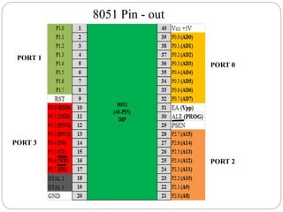
2. 8051 Pin Description
The 8051 is packaged in a 40 – pin DIP (Dual – In Line Package).
It is important to note that many pins of 8051 are used for more than
one function. The alternative functions of pins are shown in bold
letters.
It has 32 I/O pins configured as four eight – bit parallel ports (P0, P1,
P2, P3 - Bidirectional).
All ports are multiplexed except the pins of port 1.
Each port consists of a latch, an output driver and an input buffer.
3. PORT 0 (Pins 32-39):
It is used as I/O pins. The output drives and input buffers
of port 0 are used to access external memory.
Port 0 outputs the low order byte of the external memory
address, time multiplexed with the data being written or
read. Thus, port 0 can be used as a multiplexed
address/data bus.
PORT 1 (Pins 1-8):
Port 1 pins can be used only as I/O pins.
4. PORT 2 (Pins 21-28):
• The output drives of port 2 are used to access external
memory. Port 2 outputs the high order byte of the external
memory address when the address is 16 bits wide.
Otherwise, port 2 is used as an I/O port.
PORT 3 (Pins 10-17):
• All port pins of port 3 are multifunctional.
• Therefore, each pin of port 3 can be programmed to use
as I/O or as one of the alternate function. They have
special functions as
5. Symbol Position Alternate Use
RD P3.7 External Memory Read Signal
WR P3.6 External Memory Write Signal
T1 P3.5 External timer 1 Input
T0 P3.4 External timer 0 Input
INT1 P3.3 External Interrupt 1 Input
INT0 P3.2 External Interrupt 0 Input
TXD P3.1 Serial data Output
RXD P3.0 Serial data Input
Alternate Use of Pins
6. Power supply pins Vcc (Pin 40) and Vss (Pin 20):
• 8051 operates on d.c. power supply of +5v with
respect to ground. The +5v is to be connected to Pin
Vcc and ground to pin Vss with rated power supply
current of 125mA.
Oscillator Pins XTAL2 (Pin 18) and XTAL1 (Pin 19):
• For generating an internal clock signal, the external
oscillator is connected at these two pins.
7. ALE( Address Latch Enable):
• AD0 to AD7 lines are multiplexed. To demultiplex
these lines and for obtaining lower half of an address,
an external latch and ALE signal of 8051 is used.
Oscillator Pins XTAL2 (Pin 18) and XTAL1 (Pin 19):
• For generating an internal clock signal, the external
oscillator is connected at these two pins.
8. RST (Reset, Pin 9):
• This pin is used to reset 8051. For proper reset operation,
reset signal must be held high at least for two machine
cycles, while oscillator is running.
PSEN (Program Store Enable, Pin 29):
• It is the active low output control signal used to activate
the enable signal of the external ROM/EPROM. It is
activated every six oscillator periods while reading the
external memory. Thus, this signal acts as the read strobe
to external program memory.
9. EA (External Access, Pin 31):
• When this pin is high (Connected to Vcc), program
fetches to address 0000H through 0FFFH are directed
to the internal ROM and program fetches to address
1000H through FFFFH are directed to external
ROM/EPROM.
• When this pin is Low, all addresses fetched by
program are directed to the external ROM/EPROM
10. Internal and External Memories
0FFFH
1000H
60 Kbytes
External
4 Kbytes
Internal
64 Kbytes
External
EA =
0
Access
EA =
1
Access
OR
External
Memory
Internal Memory
FFFFH
0000
FFFFH
0000
Program Memory
12. • It can access up to 64K program memory and 64K
data memory.
• The 8051 has 4K bytes of internal program memory
and 256 bytes of internal data memory.
13. Internal RAM Organization
• The 8051 has 128 – byte internal RAM. It is accesses
using RAM address register.
• RAM of 8051 is organized into three distinct areas:
1. Register Bank.
2. Bit Addressable.
3. General Purpose.
14. 8051 Register Banks (Working Registers)
• The first 32-bytes from address 00H to 1FH of internal
RAM constitute 32 working registers. They are organized
into four banks of eight registers each. The four register
banks are numbered 0 to 3 and are consists of eight registers
name R0 to R7.
• Each register can be addressed by name or by its RAM
address. Only one register bank is in use at a time. Bits RS0
and RS1 in the PSW determine which bank of registers is
currently in use.
15. • On reset, the bank 0 is selected and hence it is a default
register bank. Register banks when not selected can be
used as general purpose RAM.
RS1(PSW.4) RS0 (PSW.3) Bank Selection
0 0 Bank 0
0 1 Bank 1
1 0 Bank 2
1 1 Bank 3
16.
17. Bit / Byte Addressable
• The 8051 provides 16 bytes if a bit-addressable area.
• It occupies RAM byte addresses from 20H to 2FH, forming
a total of 128(16 X 8) addressable bits.
• An addressable bit may be specified by its bit address of
00H to 7FH, or 8 bits may form any byte address from 20H
to 2FH.
• For example, bit address 4EH refers bit 6 of the byte
address 29H.
18. General Purpose RAM
• The RAM area above bit addressable area from 30H to 7FH
is called general purpose RAM. It is addressable by byte.
ROM Space in 8051
• 4 byte of internal ROM with address space from 0000H to
0FFFH. It is programmed by manufacturer when the chip is built.
This part cannot be erased and altered after fabrication. This is
used to store final version of the program.
• It is accessed using program address register.
19. The Program Status Word (PSW) register is an 8-bit
register. It is also referred to as the flag register. Although
the PSW register is 8 bits wide, only 6 bits of it are used
by the 8051.
The two unused bits are user-definable flags.
Four of the flags are called conditional flags, meaning that
they indicate some conditions that result after an
instruction is executed. These four are CY (carry), AC
(auxiliary carry),
P (parity), and OV (overflow).
20. The bits PSW.3 and PSW.4 are designated as RSO and
RSI, respectively, and are used to change the bank
registers.
The PSW.5 and PSW.l bits are general-purpose status flag
bits and can be used by the programmer for any purpose.
In other words, they are user definable.