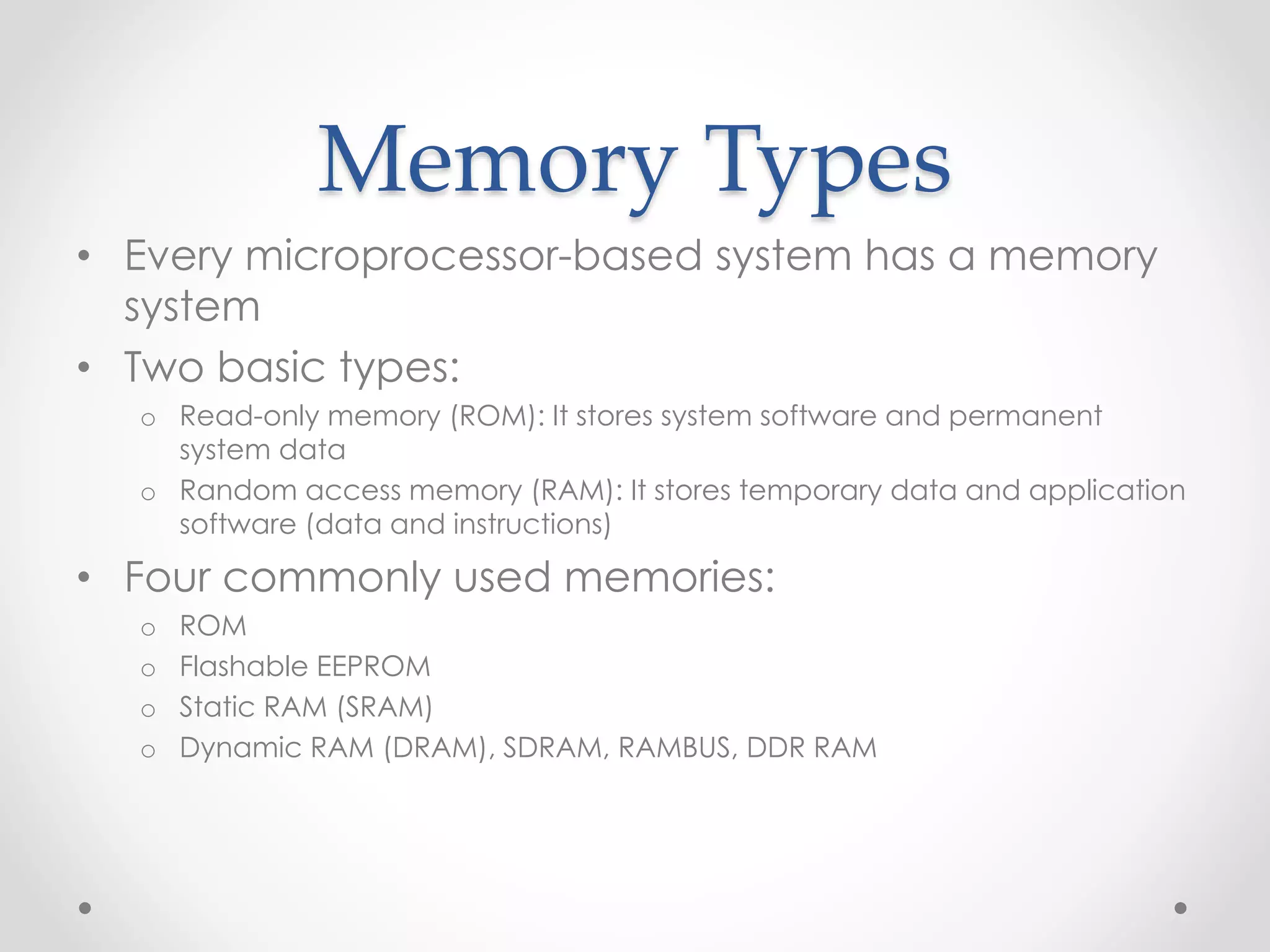
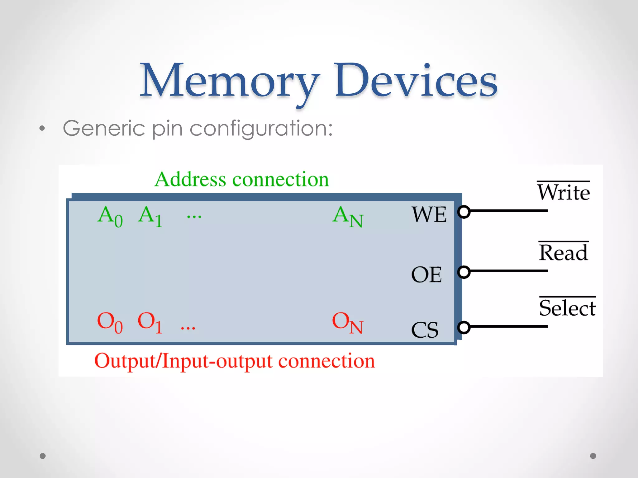
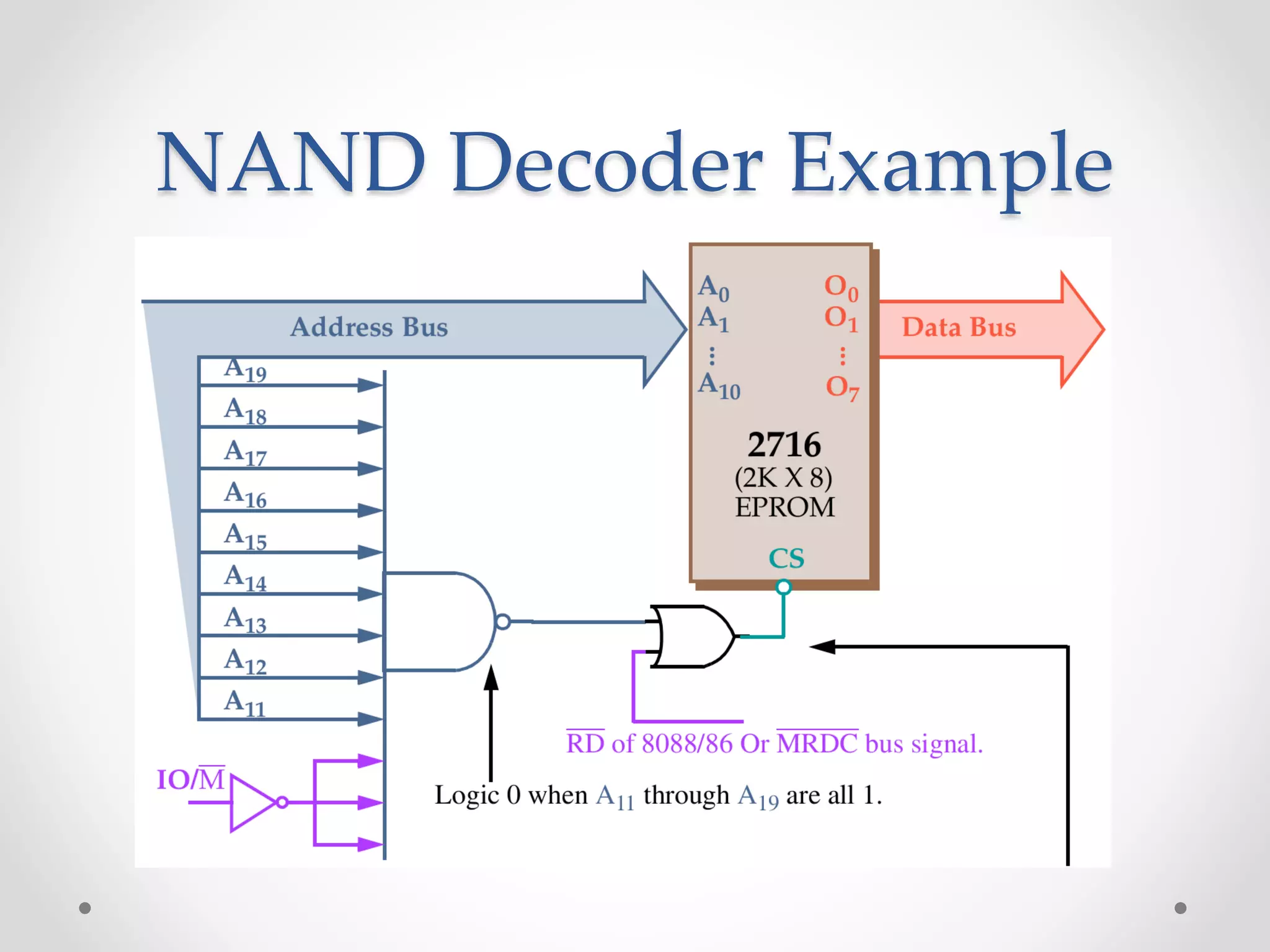
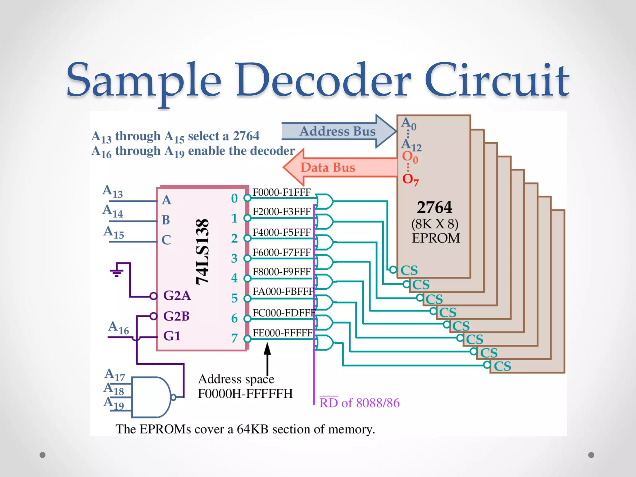
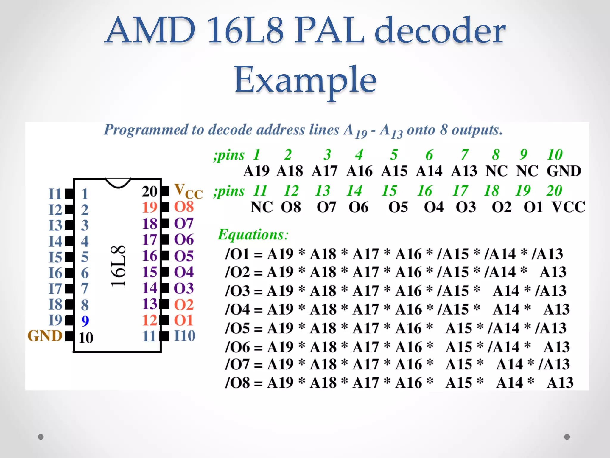
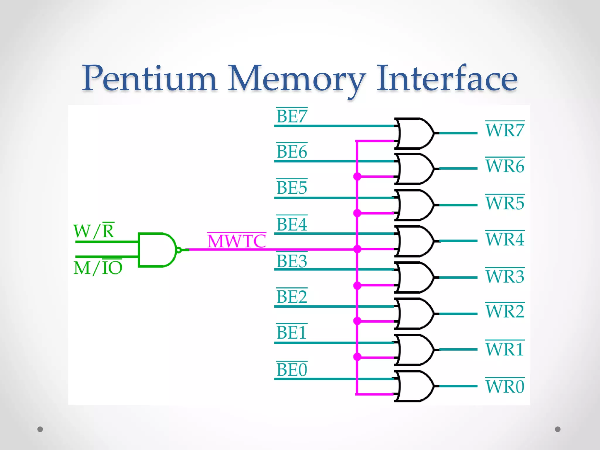
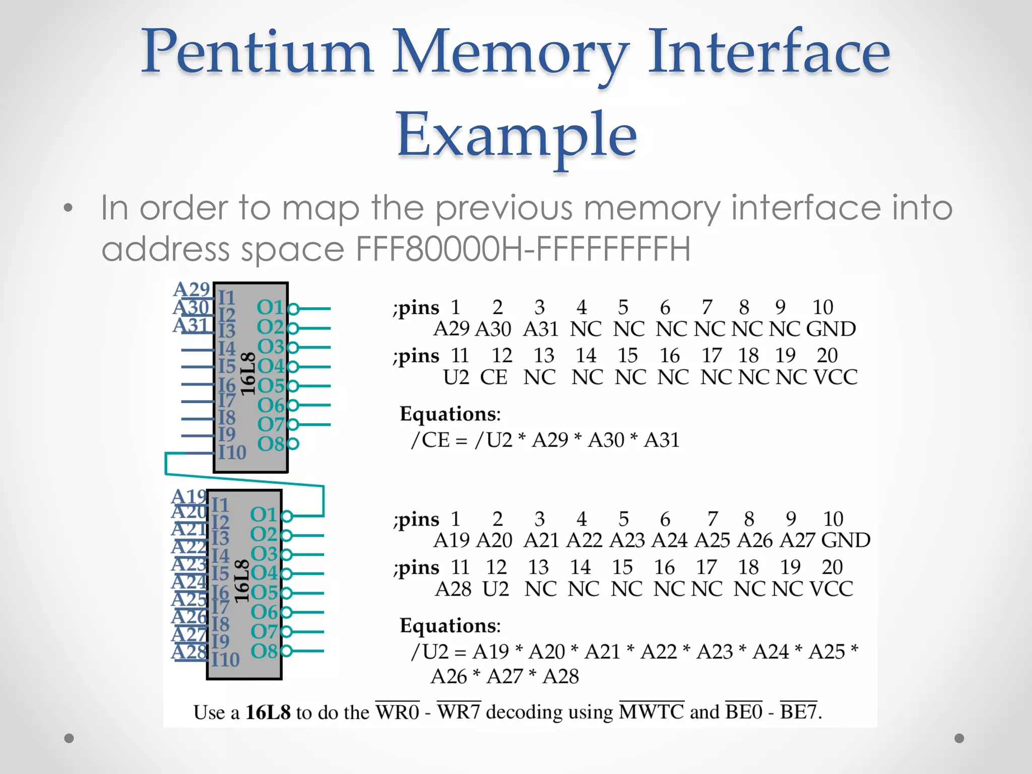
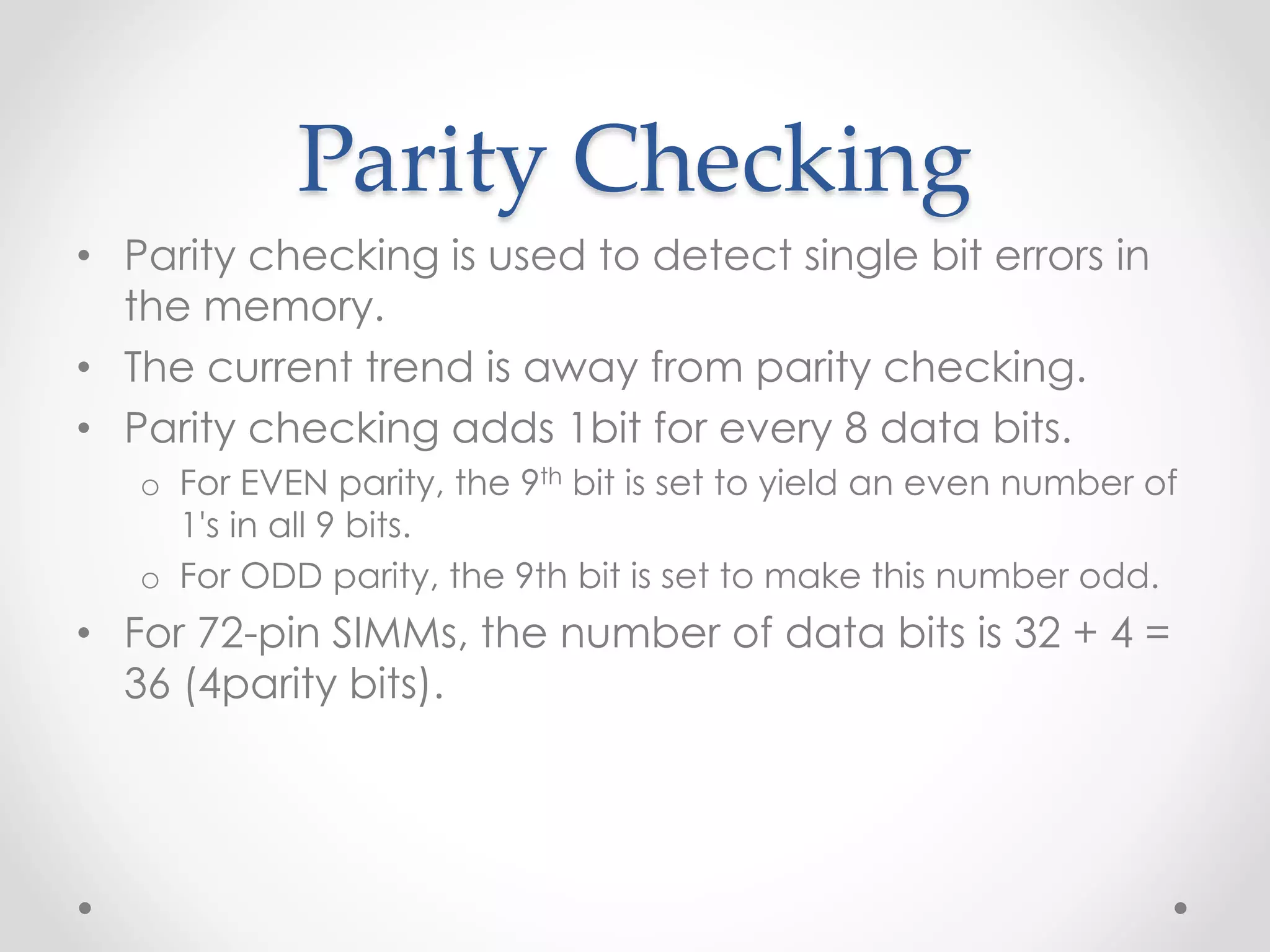
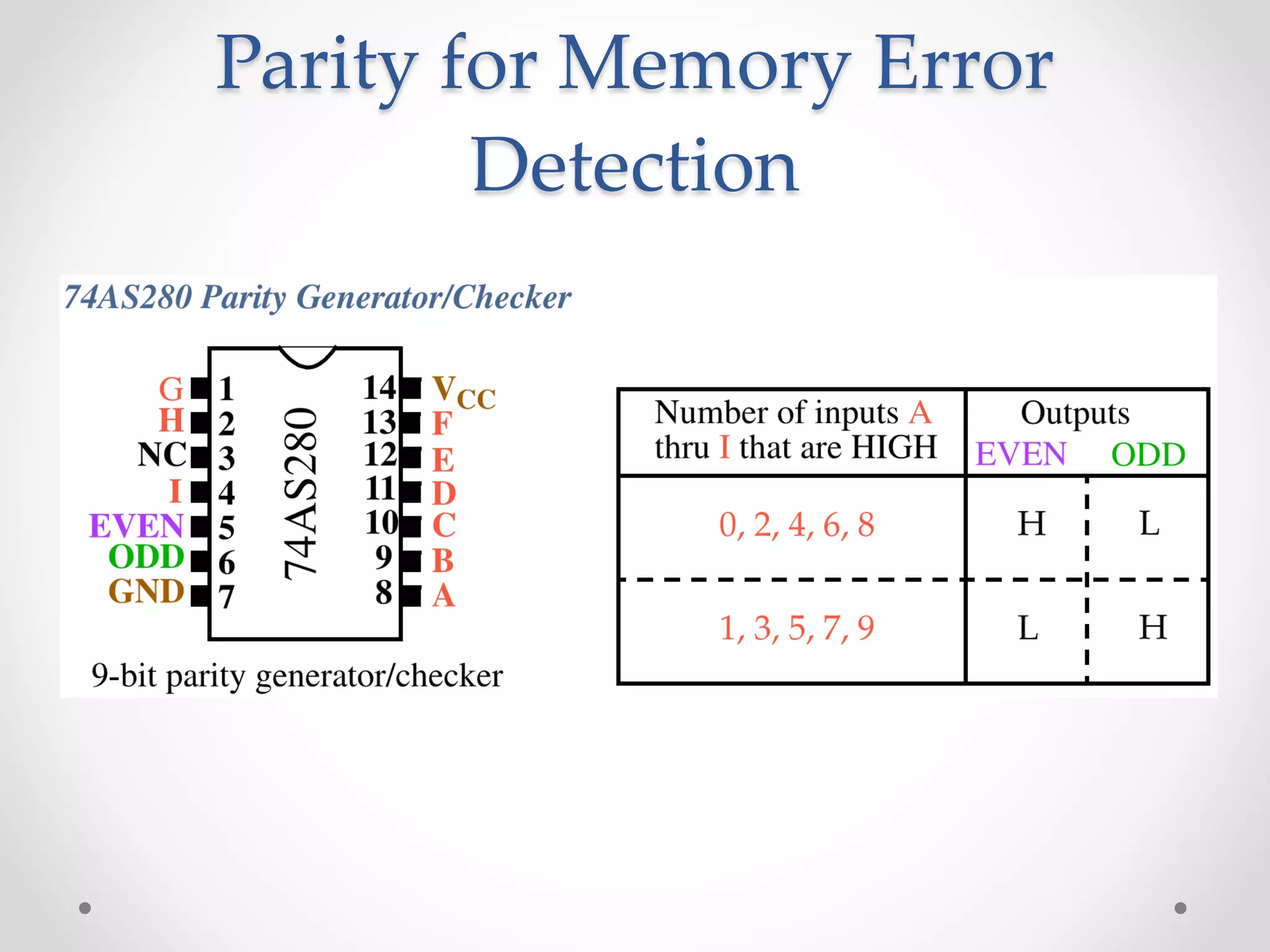
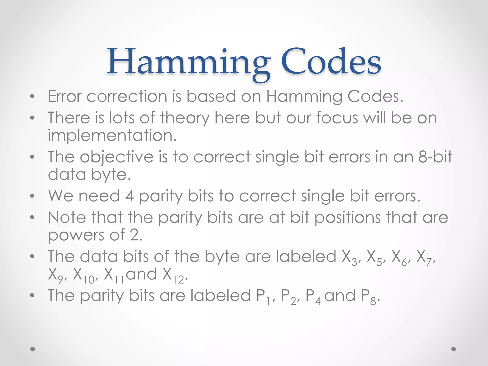
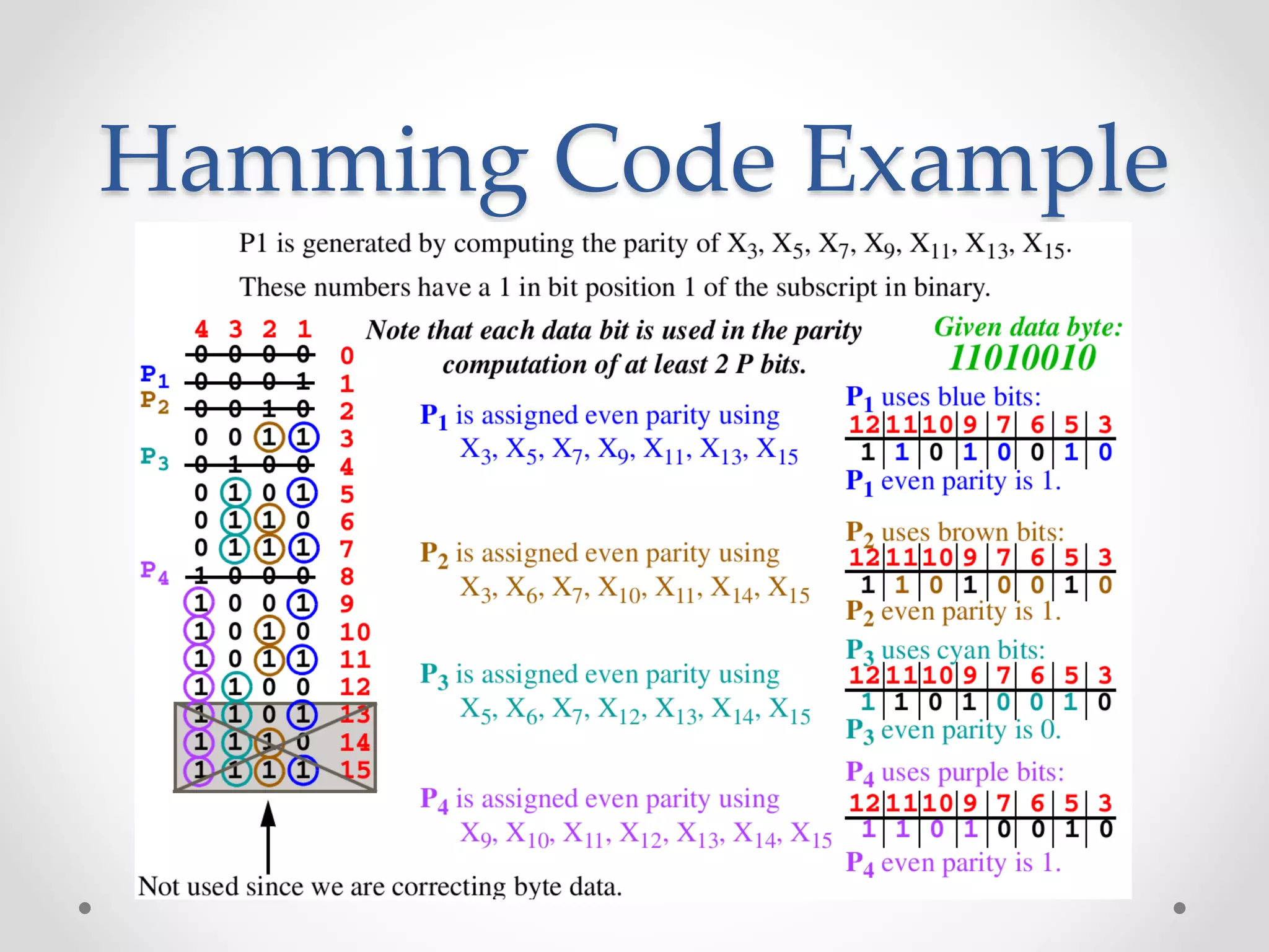
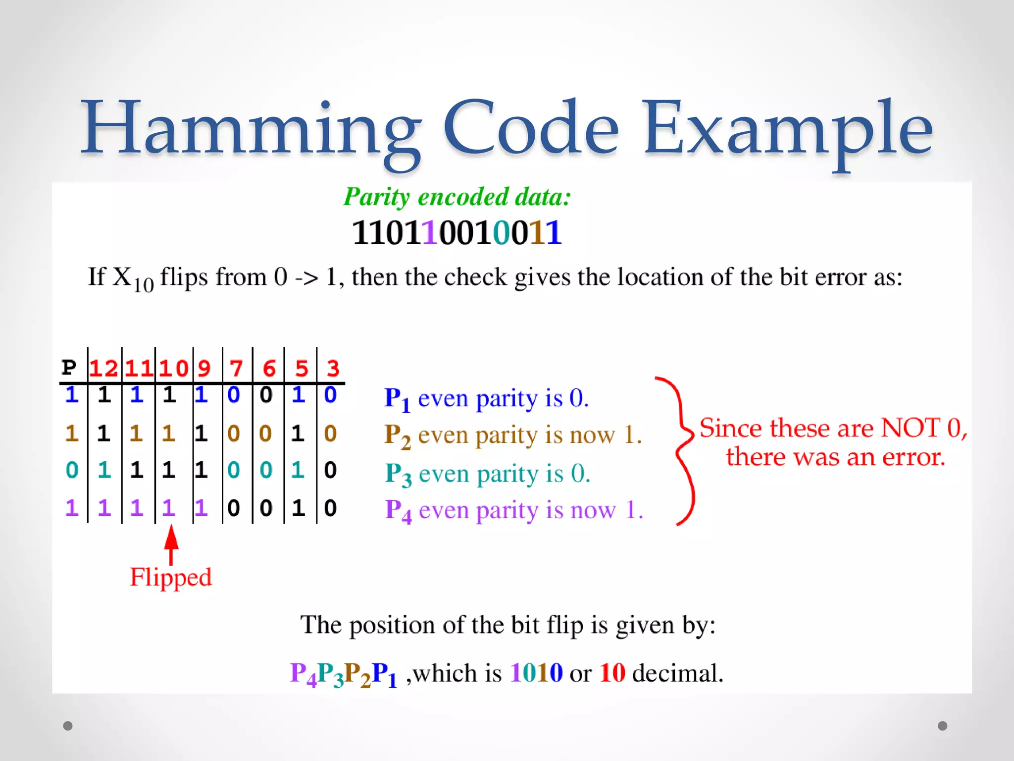
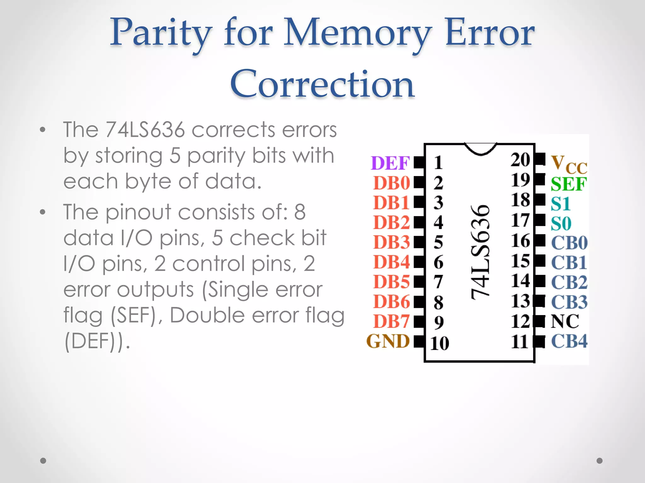
SlideShare a Scribd company logo
Memory
Interface
Dr. Mohammed Morsy
Memory Interface
• This chapter will discuss:
o Memory Devices:
ROM, EEPROM, SRAM, DRAM.
o Address Decoding.
o 8088 Memory Interface.
o 8086 Memory Interface.
Memory Types
• Every microprocessor-based system has a memory
system
• Two basic types:
o Read-only memory (ROM): It stores system software and permanent
system data
o Random access memory (RAM): It stores temporary data and application
software (data and instructions)
• Four commonly used memories:
o ROM
o Flashable EEPROM
o Static RAM (SRAM)
o Dynamic RAM (DRAM), SDRAM, RAMBUS, DDR RAM
Memory Devices
• Generic pin configuration:
Address Pins
• All memory devices have address inputs.
• They select a memory location within the memory
device.
• The number of address pins is related to the number of
memory locations.
o Common sizes today are 1K to 256M locations.
o Therefore, between 10 and 28 address pins are present.
• Address inputs are labeled from A0 to AN.
• N is the total number of address pins minus 1.
• Example: The 2K memory:
o It has 11 address lines.
o The labels are (A0 - A10).
o If the start address is 10000H so the end address is:
10000H + ((2*1024)10 = 800H)=107FFH
Data Pins
• All memory devices have a set of data outputs or
input/outputs.
• They are used to enter the data for storage or
extract the data for reading.
• The data pins are typically bi-directional in read-
write memories.
o The number of data pins is related to the size of the memory location.
o For example, an 8-bit wide (byte-wide) memory device has 8data pins.
o Catalog listing of 1K X 8 indicate a byte addressable 8Kbit memory with 10
address pins.
• Memory devices are defined by memory locations
times bit per location.
• Examples: 1K8, 16K1, 64K4.
Selection Pins
• Each memory device has at least one chip
select(𝐶𝑆) or chip enable(𝐶𝐸) or select(𝑆) pin that
enables the memory device.
o This enables read and/or write operations.
o If more than one are present, then all must be 0 in order to perform a read
or write.
• If they are active (logic 0), the memory device
performs a read or write operation.
• If they are inactive (logic 1), the memory is disabled
and do not do any operation.
• If more than one selection connection is present. All
must be activated to read or write.
Control Pins
• Each memory device has at least one control pin
• For ROMs, an Output Enable (𝑂𝐸) or Gate (𝐺) is
present.
• The 𝑂𝐸 pin enables and disables a set of tri-state
buffers.
• For RAMs, a read-write(R/𝑊) or write enable(𝑊𝐸)
and read enable(𝑂𝐸) are present.
• For dual control pin devices, it must be hold true
that both are not 0 at the same time.
ROMs
• Non-volatile memory: Maintains its state when
powered down.
• There are several forms:
o ROM: Factory programmed, cannot be changed. Older style.
o Programmable Read-Only Memory (PROM): Field programmable but only
once. Older style.
o Erasable Programmable Read-Only Memory (EPROM): Reprogramming
requires up to 20 minutes of high-intensity UV light exposure.
o Electrically Erasable Programmable ROM (EEPROM): Also called
Electrically Alterable ROM (EAROM) and NOVRAM (Non-Volatile RAM).
Writing is much slower than a normal RAM.
Used to store setup information, e.g. video card, on computer systems.
Can be used to replace EPROM for BIOS memory.
ROMs
• The 27XXX series of the EPROM includes:
o 2704 (512  8). 2708 (1K  8).
o 2716 (2K  8). 2732 (4K  8).
o 2764 (8K  8). 27128 (16K  8).
o 27256 (32K  8). 27512 (64K  8).
o 271024 (128K  8).
• Each EPROM has:
o Address pins
o 8 data connections
o One or more selection inputs and one output
enable pin.
Intel 2716 EPROM (2K X 8)
SRAM
• SRAMs are virtually identical to the EPROM with
respect to the pinout although access time is faster
(250ns).
• SRAMs used for caches have access times as low as
10ns.
DRAM
• SRAMs are limited in size (up to about 128K X 8).
• DRAMs are available in much larger sizes, e.g., 64M X 1.
• DRAMs MUST be refreshed (rewritten) every 2 to 4 ms
Since they store their value on an integrated capacitor
that loses charge over time.
• This refresh is performed by a special circuit in the DRAM
which refreshes the entire memory.
• Refresh also occurs on a normal read or write.
• The large storage capacity of DRAMs make it
impractical to add the required number of address pins.
• Instead, the address pins are multiplexed.
TI TMS4464 DRAM (64K X 4)
• The TMS4464 can store a total of 256K bits of data.
• It has 64Kaddressable locations which means it
needs 16 address inputs, but it has only 8.
• The row address (A0 through A7) are placed on the
address pins and strobed into a set of internal
latches.
• The column address (A8 through A15) is then strobed
in using 𝐶𝐴𝑆.
TI TMS4464 DRAM (64K X 4)
Timing Diagram:
DRAMs
• Larger DRAMs are available which are organized as
1M X 1, 4M X 1, 16M X 1, 64M X 1, 256M X 1.
• DRAMs are typically placed on SIMM (Single In-line
Memory Modules) or DIMM (Dual In-line Memory
Modules) boards.
Memory Address Decoding
• The processor can usually address a memory space that
is much larger than the memory space covered by an
individual memory chip.
• In order to splice a memory device into the address
space of the processor, decoding is necessary.
• For example, the 8088 issues 20-bit addresses for a total
of 1MB of memory address space.
• However, the BIOS on a 2716 EPROM has only 2KB of
memory and 11address pins.
• A decoder can be used to decode the additional 9
address pins and allow the EPROM to be
• placed in any 2KB section of the 1MB address space.
NAND Decoder Example
• To determine the address range that a
device is mapped into
• NAND gate decoders are not often used
o Large fan-in NAND gates are not efficient
o Multiple NAND gate IC's might be required to perform such
decoding
o Rather the 3-to-8 Line Decoder (74LS138) is more common.
The 3-to-8 Line Decoder
(74LS138)
Sample Decoder Circuit
Dual 2-to-4 Line Decoder
• 74LS139 is a dual 2-to-4 line decoder
Programmable Decoder
• Programmable Logic Devices (PLDs) can be used
as a decoder
• PLDs come in three varieties:
o PLA (Programmable Logic Array)
o PAL (Programmable Array Logic)
o GAL (Gated Array Logic)
• PLDs have been around since the mid-1970s but
have only recently appeared in memory systems
(PALs have replaced PROM address decoders).
• PALs and PLAs can be fuse-programmed (like the
PROM) or erasable (like the EPROM).
AMD 16L8 PAL decoder
Example
8088 and 80188 (8-bit)
Memory Interface
• The memory system "sees" the 8088 as a
device with:
o 20 address connections (A19 to A0).
o 8 data bus connections (AD7 to AD0).
o 3 control signals: IO/𝑀, 𝑅𝐷, and 𝑊𝑅.
• We'll present examples of the 8088 interfacing
with:
o 32K of EPROM (at addresses F8000H through
FFFFFH).
o 512K of SRAM (at addresses 00000H through 7FFFFH).
8088 and 80188 (8-bit) EPROM
Memory Interface Example
• The EPROM interface uses a 74LS138 (3-to-8
line decoder) plus 8 2732 ( 4K X 8 ) EPROMs.
• The EPROM will also require the generation of
a wait state.
o The EPROM has an access time of 450ns .
o The 74LS138 requires 12ns to decode.
o The 8088 runs at 5MHz and only allows 460ns for
memory to access data.
o A wait state adds 200ns of additional time
8088 and 80188 (8-bit) EPROM
Memory Interface Example
8088 and 80188 (8-bit) SRAM
Memory Interface Example
8086,80186, 80286 and 80386
Memory Interface
• These machines differ from the
8088/80188 in several ways:
o The data bus is 16-bitswide.
o The IO/𝑀 pin is replaced with M/𝐼𝑂 (8086/80186) and 𝑀𝑅𝐷𝐶
and 𝑀𝑊𝑇𝐶 for 80286 and 80386SX.
o 𝐵𝐻𝐸, Bus High Enable, control signal is added.
o Address pin A0 (or 𝐵𝐿𝐸, Bus Low Enable) is used differently.
• The 16-bit data bus presents a new problem:
o The microprocessor must be able to read and write data
to any 16-bit location in addition to any 8-bit location.
8086,80186, 80286 and 80386
Memory Interface
• The data bus and memory are divided into banks:
• BHE and BLE are used to select one or both:
8086,80186, 80286 and 80386
Memory Interface
• Bank selection can be accomplished in two ways:
o Separate write decoders for each bank (which drive 𝐶𝑆).
o A separate write signal (strobe) to each bank (which drive
𝑊𝐸).
Note that 8-bit read requests in this scheme are handled by
the microprocessor (it selects the bits it wants to read from
the 16-bits on the bus).
• It does not seem to be a big difference between
these methods.
• Note in either method that A0 does not connect to
memory and bus wire A1 connects to memory pin
A0, A2 to A1, etc.
80386SX 16-bit Memory Interface
Example (Separate Decoders)
80386DX and 80486 Memory
Interface
• 80386DX and 80486 have 32-bit data buses and
therefore 4 banks of memory.
• 32-bit, 16-bitand 8-bit transfers are accomplished by
different combinations of the bank selection signals
𝐵𝐸3, 𝐵𝐸2, 𝐵𝐸1, 𝐵𝐸0.
• The Address bits A0 and A1are used within the
microprocessor to generate these signals.
• They are don't cares in the decoding of the 32-bit
address outside the chip (using a PLD such as the
PAL 16L8).
• The high clock rates of these processors usually
require wait states for memory access.
Pentium Memory Interface
• The Pentium, Pentium Pro, Pentium II and III contain
a 64-bit data bus.
• Therefore, 8 decoders or 8 write strobes are needed
as well as 8 memory banks.
• The write strobes are obtained by combining the
bank enable signals (𝐵𝐸𝑥) with the 𝑀𝑊𝑇𝐶 signal.
• 𝑀𝑊𝑇𝐶 is generated by combining the M/𝐼𝑂 and
W/𝑅 signals.
Pentium Memory Interface
Example
Pentium Memory Interface
Example
• In order to map the previous memory interface into
address space FFF80000H-FFFFFFFFH
Error Detection and Correction
in Memory Devices
• Memory devices use error detection and correction
methods to detect and correct memory storing
errors.
• Error detection and correction methods attach
extra bits to data strings which can help in error
detection and correction.
• In this section we will discuss:
o Parity checking
o Checksum tests
o Cyclic Redundancy Check
o Hamming code error correction
Parity Checking
• Parity checking is used to detect single bit errors in
the memory.
• The current trend is away from parity checking.
• Parity checking adds 1bit for every 8 data bits.
o For EVEN parity, the 9th bit is set to yield an even number of
1's in all 9 bits.
o For ODD parity, the 9th bit is set to make this number odd.
• For 72-pin SIMMs, the number of data bits is 32 + 4 =
36 (4parity bits).
Parity for Memory Error
Detection
Parity for Memory Error
Detection
• This circuit generates EVEN or ODD parity for the 9-
bit number placed on its inputs.
• Typically, for generation, the 9th input bit is set to 0.
• This circuit also checks EVEN or ODD parity for the 9-
bit number.
• In this case, the 9th input bit is connected to the 9th
bit of memory.
• For example, if the original byte has an even # of 1's
(with 9th bit at GND), the parity bit is set to 1 (from
the EVEN output).
• If the EVEN output goes high during the check, then
an error occurred.
Parity for Memory Error
Detection
Checksum Error Detection
• This parity scheme can only detect a single bit error.
• Block-Check Character (BCC) or Checksum can
detect multiple bit errors.
• This is simply the two's complement sum (the
negative of the sum) of the sequence of bytes.
• No error occurred if adding the data values and
the checksum produces a 0.
Checksum Error Detection
• For example
• If 45 changes to 44 AND 04 changes to 05, the error
is missed.
CRC Error Detection
• Cyclic Redundancy Check (CRC) is commonly
used to check data transfers in hardware such as
hard drives.
• Treats data as a stream of serial data n-bits long.
• The bits are treated as coefficients of a
characteristic polynomial, M(X) of the form:
where b0 is the least significant bit while bn is
the most significant bit.
CRC Error Detection
• For example
• The CRC is found by applying the following equation
• G(X)is the called the generator polynomial and has
special properties.
CRC Error Detection
• A commonly used polynomial is:
• The remainder R(X) is appended to the data block.
• When the CRC and R(X)is computed by the
receiver, R(X)should be zero.
• Since G(X)is of power 16, the remainder, R(X),
cannot be of order higher than 15.
• Therefore, no more than 2 bytes are needed
independent of the data block size.
CRC Error Detection Example
• For the data stream 26F0H:
Error Correction
• Parity, BCC and CRC are only mechanisms for error
detection.
• The system is halted if an error is found in memory.
• Error correction is starting to show up in new
systems.
• SDRAM has ECC (Error Correction Code).
• Correction will allow the system to continue its
operation.
• If two errors occur, they can be detected but not
corrected.
• Error correction will of course cost more in terms of
extra bits.
Hamming Codes
• Error correction is based on Hamming Codes.
• There is lots of theory here but our focus will be on
implementation.
• The objective is to correct single bit errors in an 8-bit
data byte.
• We need 4 parity bits to correct single bit errors.
• Note that the parity bits are at bit positions that are
powers of 2.
• The data bits of the byte are labeled X3, X5, X6, X7,
X9, X10, X11and X12.
• The parity bits are labeled P1, P2, P4 and P8.
Calculating the Hamming
Code
The key to the Hamming Code is the use of extra parity bits to allow the
identification of a single error. Create the code word as follows:
• Mark all bit positions that are powers of two as parity bits.(positions 1, 2, 4,
8, 16, etc)
• All other bit positions are for the data to be encoded. (positions 3, 5, 6, 7,
9, 10, 11, 12, 13, 14, 15, 17, etc.)
• Each parity bit calculates the parity for some of the bits in the code word.
The position of the parity bit determines the sequence of bits that it
alternately checks and skips.
Position 1: check 1 bit, skip 1 bit, check 1 bit, skip 1 bit, etc. (1, 3, 5, 7, 9,
11, 13, 15,...)
Position 2: check 2 bits, skip 2 bits, check 2 bits, skip 2 bits, etc.(2, 3, 6, 7,
10, 11, 15,...)
Position 4: check 4 bits, skip 4 bits, check 4 bits, skip 4 bits, etc. (4, 5, 6, 7,
12, 13, 14, 15, 20, 21, 22, 23, ...)
Position 8: check 8 bits, skip 8 bits, check 8 bits, skip 8 bits, etc. (8-15, 24-
31, 40-47,...)
• Set a parity bit to 1 if the total number of ones in the positions it checks is
odd. Set a parity bit to 0 if the total number of ones in the positions it
checks is even.
Hamming Code Example
Parity for Memory Error
Correction
• The 74LS636 corrects errors
by storing 5 parity bits with
each byte of data.
• The pinout consists of: 8
data I/O pins, 5 check bit
I/O pins, 2 control pins, 2
error outputs (Single error
flag (SEF), Double error flag
(DEF)).

More Related Content

What's hot

8086 in minimum mode
8086 in minimum mode8086 in minimum mode
8086 in minimum mode
Sridari Iyer
 
Bus aribration
Bus aribrationBus aribration
Bus aribration
Saiyam Agrawal
 
Programmers model of 8086
Programmers model of 8086Programmers model of 8086
Programmers model of 8086
KunalPatel260
 
8251 USART
8251 USART8251 USART
8251 USART
ShivamSood22
 
Bus Structure, Memory and I/O Interfacing
Bus Structure, Memory and I/O InterfacingBus Structure, Memory and I/O Interfacing
Bus Structure, Memory and I/O Interfacing
Hetauda City College
 
Topic : X.25, Frame relay and ATM
Topic :  X.25, Frame relay and ATMTopic :  X.25, Frame relay and ATM
Topic : X.25, Frame relay and ATM
Dr Rajiv Srivastava
 
Hamming code system
Hamming code systemHamming code system
Hamming code system
DILSHAD AHMAD
 
8051 serial communication
8051 serial communication8051 serial communication
8051 serial communicationasteriskbimal
 
Semiconductor memories
Semiconductor memoriesSemiconductor memories
Semiconductor memoriesSambitShreeman
 
Microprocessor 8086
Microprocessor 8086Microprocessor 8086
Microprocessor 8086
Gopikrishna Madanan
 
Serial Communication In Atmega 16
Serial Communication In Atmega 16Serial Communication In Atmega 16
Serial Communication In Atmega 16Suren Kumar
 
8255 Programmable parallel I/O
8255 Programmable parallel I/O 8255 Programmable parallel I/O
8255 Programmable parallel I/O
Muhammed Afsal Villan
 
Token bus
Token busToken bus
Token bus
Denver Rockfreak
 
Direct Memory Access(DMA)
Direct Memory Access(DMA)Direct Memory Access(DMA)
Direct Memory Access(DMA)
Page Maker
 
Timing and-control-unit
Timing and-control-unitTiming and-control-unit
Timing and-control-unitAnuj Modi
 
The Intel 8086 microprocessor
The Intel 8086 microprocessorThe Intel 8086 microprocessor
The Intel 8086 microprocessor
George Thomas
 
Interfacing memory with 8086 microprocessor
Interfacing memory with 8086 microprocessorInterfacing memory with 8086 microprocessor
Interfacing memory with 8086 microprocessor
Vikas Gupta
 

What's hot (20)

8086 in minimum mode
8086 in minimum mode8086 in minimum mode
8086 in minimum mode
 
Bus aribration
Bus aribrationBus aribration
Bus aribration
 
Programmers model of 8086
Programmers model of 8086Programmers model of 8086
Programmers model of 8086
 
DMA and DMA controller
DMA and DMA controllerDMA and DMA controller
DMA and DMA controller
 
8251 USART
8251 USART8251 USART
8251 USART
 
Coding
CodingCoding
Coding
 
Bus Structure, Memory and I/O Interfacing
Bus Structure, Memory and I/O InterfacingBus Structure, Memory and I/O Interfacing
Bus Structure, Memory and I/O Interfacing
 
Topic : X.25, Frame relay and ATM
Topic :  X.25, Frame relay and ATMTopic :  X.25, Frame relay and ATM
Topic : X.25, Frame relay and ATM
 
8259 updated
8259 updated 8259 updated
8259 updated
 
Hamming code system
Hamming code systemHamming code system
Hamming code system
 
8051 serial communication
8051 serial communication8051 serial communication
8051 serial communication
 
Semiconductor memories
Semiconductor memoriesSemiconductor memories
Semiconductor memories
 
Microprocessor 8086
Microprocessor 8086Microprocessor 8086
Microprocessor 8086
 
Serial Communication In Atmega 16
Serial Communication In Atmega 16Serial Communication In Atmega 16
Serial Communication In Atmega 16
 
8255 Programmable parallel I/O
8255 Programmable parallel I/O 8255 Programmable parallel I/O
8255 Programmable parallel I/O
 
Token bus
Token busToken bus
Token bus
 
Direct Memory Access(DMA)
Direct Memory Access(DMA)Direct Memory Access(DMA)
Direct Memory Access(DMA)
 
Timing and-control-unit
Timing and-control-unitTiming and-control-unit
Timing and-control-unit
 
The Intel 8086 microprocessor
The Intel 8086 microprocessorThe Intel 8086 microprocessor
The Intel 8086 microprocessor
 
Interfacing memory with 8086 microprocessor
Interfacing memory with 8086 microprocessorInterfacing memory with 8086 microprocessor
Interfacing memory with 8086 microprocessor
 

Similar to Memory_Interface.pdf

05 basic io_operation_part01
05 basic io_operation_part0105 basic io_operation_part01
05 basic io_operation_part01
Hetauda City College
 
901320_Main Memory.ppt
901320_Main Memory.ppt901320_Main Memory.ppt
901320_Main Memory.ppt
Chandinialla1
 
Memory And Storages
Memory And StoragesMemory And Storages
Memory And Storages
Arsalan Qureshi
 
Computer Organisation and Architecture
Computer Organisation and ArchitectureComputer Organisation and Architecture
Computer Organisation and Architecture
Subhasis Dash
 
Computer organization memory
Computer organization memoryComputer organization memory
Computer organization memory
Deepak John
 
Microprocessor Part 1
Microprocessor    Part 1Microprocessor    Part 1
Microprocessor Part 1
Sajan Agrawal
 
DIGITAL DESIGNS SLIDES 7 ENGINEERING 2ND YEAR
DIGITAL DESIGNS SLIDES 7 ENGINEERING  2ND YEARDIGITAL DESIGNS SLIDES 7 ENGINEERING  2ND YEAR
DIGITAL DESIGNS SLIDES 7 ENGINEERING 2ND YEAR
kasheen2803
 
sramanddram.ppt
sramanddram.pptsramanddram.ppt
sramanddram.ppt
AmalNath44
 
Part of UNIT2 Memory mapped IOjkl;'lk.pdf
Part of UNIT2 Memory mapped IOjkl;'lk.pdfPart of UNIT2 Memory mapped IOjkl;'lk.pdf
Part of UNIT2 Memory mapped IOjkl;'lk.pdf
Abhishekkumar397974
 
Lec 3 digital electronics- read only memory
Lec 3  digital electronics- read only memoryLec 3  digital electronics- read only memory
Lec 3 digital electronics- read only memory
priyankatabhane
 
address decoding.pdf
address decoding.pdfaddress decoding.pdf
address decoding.pdf
AbirAbedin
 
Memory interface
Memory interfaceMemory interface
Memory interface
Dr. Girish GS
 
memory-interfacing.ppt
memory-interfacing.pptmemory-interfacing.ppt
memory-interfacing.ppt
Vanitha472439
 
Core Hardware: Lecture 4
Core Hardware: Lecture 4Core Hardware: Lecture 4
Core Hardware: Lecture 4
Awinash Goswami
 
Unit IV Memory.pptx
Unit IV  Memory.pptxUnit IV  Memory.pptx
Unit IV Memory.pptx
madhukarvnimbalkar
 
Chapter 2-8085 Microprocessor Architecture and Microcomputer Systems
Chapter 2-8085 Microprocessor Architecture and Microcomputer SystemsChapter 2-8085 Microprocessor Architecture and Microcomputer Systems
Chapter 2-8085 Microprocessor Architecture and Microcomputer Systems
cmkandemir
 
8051 architecture and pin configuration
8051 architecture and pin configuration8051 architecture and pin configuration
8051 architecture and pin configuration
NITHIN KALLE PALLY
 
EPROM, PROM & ROM
EPROM, PROM & ROMEPROM, PROM & ROM
EPROM, PROM & ROM
Abhilash Nair
 

Similar to Memory_Interface.pdf (20)

05 basic io_operation_part01
05 basic io_operation_part0105 basic io_operation_part01
05 basic io_operation_part01
 
901320_Main Memory.ppt
901320_Main Memory.ppt901320_Main Memory.ppt
901320_Main Memory.ppt
 
Memory And Storages
Memory And StoragesMemory And Storages
Memory And Storages
 
Computer Organisation and Architecture
Computer Organisation and ArchitectureComputer Organisation and Architecture
Computer Organisation and Architecture
 
Computer organization memory
Computer organization memoryComputer organization memory
Computer organization memory
 
Microprocessor Part 1
Microprocessor    Part 1Microprocessor    Part 1
Microprocessor Part 1
 
DIGITAL DESIGNS SLIDES 7 ENGINEERING 2ND YEAR
DIGITAL DESIGNS SLIDES 7 ENGINEERING  2ND YEARDIGITAL DESIGNS SLIDES 7 ENGINEERING  2ND YEAR
DIGITAL DESIGNS SLIDES 7 ENGINEERING 2ND YEAR
 
sramanddram.ppt
sramanddram.pptsramanddram.ppt
sramanddram.ppt
 
Chapter 9
Chapter 9Chapter 9
Chapter 9
 
Part of UNIT2 Memory mapped IOjkl;'lk.pdf
Part of UNIT2 Memory mapped IOjkl;'lk.pdfPart of UNIT2 Memory mapped IOjkl;'lk.pdf
Part of UNIT2 Memory mapped IOjkl;'lk.pdf
 
Lec 3 digital electronics- read only memory
Lec 3  digital electronics- read only memoryLec 3  digital electronics- read only memory
Lec 3 digital electronics- read only memory
 
address decoding.pdf
address decoding.pdfaddress decoding.pdf
address decoding.pdf
 
Memory interface
Memory interfaceMemory interface
Memory interface
 
memory-interfacing.ppt
memory-interfacing.pptmemory-interfacing.ppt
memory-interfacing.ppt
 
Memoryhierarchy
MemoryhierarchyMemoryhierarchy
Memoryhierarchy
 
Core Hardware: Lecture 4
Core Hardware: Lecture 4Core Hardware: Lecture 4
Core Hardware: Lecture 4
 
Unit IV Memory.pptx
Unit IV  Memory.pptxUnit IV  Memory.pptx
Unit IV Memory.pptx
 
Chapter 2-8085 Microprocessor Architecture and Microcomputer Systems
Chapter 2-8085 Microprocessor Architecture and Microcomputer SystemsChapter 2-8085 Microprocessor Architecture and Microcomputer Systems
Chapter 2-8085 Microprocessor Architecture and Microcomputer Systems
 
8051 architecture and pin configuration
8051 architecture and pin configuration8051 architecture and pin configuration
8051 architecture and pin configuration
 
EPROM, PROM & ROM
EPROM, PROM & ROMEPROM, PROM & ROM
EPROM, PROM & ROM
 

Recently uploaded

Final project report on grocery store management system..pdf
Final project report on grocery store management system..pdfFinal project report on grocery store management system..pdf
Final project report on grocery store management system..pdf
Kamal Acharya
 
一比一原版(IIT毕业证)伊利诺伊理工大学毕业证成绩单专业办理
一比一原版(IIT毕业证)伊利诺伊理工大学毕业证成绩单专业办理一比一原版(IIT毕业证)伊利诺伊理工大学毕业证成绩单专业办理
一比一原版(IIT毕业证)伊利诺伊理工大学毕业证成绩单专业办理
zwunae
 
H.Seo, ICLR 2024, MLILAB, KAIST AI.pdf
H.Seo,  ICLR 2024, MLILAB,  KAIST AI.pdfH.Seo,  ICLR 2024, MLILAB,  KAIST AI.pdf
H.Seo, ICLR 2024, MLILAB, KAIST AI.pdf
MLILAB
 
Sachpazis:Terzaghi Bearing Capacity Estimation in simple terms with Calculati...
Sachpazis:Terzaghi Bearing Capacity Estimation in simple terms with Calculati...Sachpazis:Terzaghi Bearing Capacity Estimation in simple terms with Calculati...
Sachpazis:Terzaghi Bearing Capacity Estimation in simple terms with Calculati...
Dr.Costas Sachpazis
 
Student information management system project report ii.pdf
Student information management system project report ii.pdfStudent information management system project report ii.pdf
Student information management system project report ii.pdf
Kamal Acharya
 
AP LAB PPT.pdf ap lab ppt no title specific
AP LAB PPT.pdf ap lab ppt no title specificAP LAB PPT.pdf ap lab ppt no title specific
AP LAB PPT.pdf ap lab ppt no title specific
BrazilAccount1
 
Nuclear Power Economics and Structuring 2024
Nuclear Power Economics and Structuring 2024Nuclear Power Economics and Structuring 2024
Nuclear Power Economics and Structuring 2024
Massimo Talia
 
ML for identifying fraud using open blockchain data.pptx
ML for identifying fraud using open blockchain data.pptxML for identifying fraud using open blockchain data.pptx
ML for identifying fraud using open blockchain data.pptx
Vijay Dialani, PhD
 
MCQ Soil mechanics questions (Soil shear strength).pdf
MCQ Soil mechanics questions (Soil shear strength).pdfMCQ Soil mechanics questions (Soil shear strength).pdf
MCQ Soil mechanics questions (Soil shear strength).pdf
Osamah Alsalih
 
Investor-Presentation-Q1FY2024 investor presentation document.pptx
Investor-Presentation-Q1FY2024 investor presentation document.pptxInvestor-Presentation-Q1FY2024 investor presentation document.pptx
Investor-Presentation-Q1FY2024 investor presentation document.pptx
AmarGB2
 
Gen AI Study Jams _ For the GDSC Leads in India.pdf
Gen AI Study Jams _ For the GDSC Leads in India.pdfGen AI Study Jams _ For the GDSC Leads in India.pdf
Gen AI Study Jams _ For the GDSC Leads in India.pdf
gdsczhcet
 
The Benefits and Techniques of Trenchless Pipe Repair.pdf
The Benefits and Techniques of Trenchless Pipe Repair.pdfThe Benefits and Techniques of Trenchless Pipe Repair.pdf
The Benefits and Techniques of Trenchless Pipe Repair.pdf
Pipe Restoration Solutions
 
The role of big data in decision making.
The role of big data in decision making.The role of big data in decision making.
The role of big data in decision making.
ankuprajapati0525
 
ethical hacking in wireless-hacking1.ppt
ethical hacking in wireless-hacking1.pptethical hacking in wireless-hacking1.ppt
ethical hacking in wireless-hacking1.ppt
Jayaprasanna4
 
space technology lecture notes on satellite
space technology lecture notes on satellitespace technology lecture notes on satellite
space technology lecture notes on satellite
ongomchris
 
Railway Signalling Principles Edition 3.pdf
Railway Signalling Principles Edition 3.pdfRailway Signalling Principles Edition 3.pdf
Railway Signalling Principles Edition 3.pdf
TeeVichai
 
CME397 Surface Engineering- Professional Elective
CME397 Surface Engineering- Professional ElectiveCME397 Surface Engineering- Professional Elective
CME397 Surface Engineering- Professional Elective
karthi keyan
 
Pile Foundation by Venkatesh Taduvai (Sub Geotechnical Engineering II)-conver...
Pile Foundation by Venkatesh Taduvai (Sub Geotechnical Engineering II)-conver...Pile Foundation by Venkatesh Taduvai (Sub Geotechnical Engineering II)-conver...
Pile Foundation by Venkatesh Taduvai (Sub Geotechnical Engineering II)-conver...
AJAYKUMARPUND1
 
Planning Of Procurement o different goods and services
Planning Of Procurement o different goods and servicesPlanning Of Procurement o different goods and services
Planning Of Procurement o different goods and services
JoytuBarua2
 
English lab ppt no titlespecENG PPTt.pdf
English lab ppt no titlespecENG PPTt.pdfEnglish lab ppt no titlespecENG PPTt.pdf
English lab ppt no titlespecENG PPTt.pdf
BrazilAccount1
 

Recently uploaded (20)

Final project report on grocery store management system..pdf
Final project report on grocery store management system..pdfFinal project report on grocery store management system..pdf
Final project report on grocery store management system..pdf
 
一比一原版(IIT毕业证)伊利诺伊理工大学毕业证成绩单专业办理
一比一原版(IIT毕业证)伊利诺伊理工大学毕业证成绩单专业办理一比一原版(IIT毕业证)伊利诺伊理工大学毕业证成绩单专业办理
一比一原版(IIT毕业证)伊利诺伊理工大学毕业证成绩单专业办理
 
H.Seo, ICLR 2024, MLILAB, KAIST AI.pdf
H.Seo,  ICLR 2024, MLILAB,  KAIST AI.pdfH.Seo,  ICLR 2024, MLILAB,  KAIST AI.pdf
H.Seo, ICLR 2024, MLILAB, KAIST AI.pdf
 
Sachpazis:Terzaghi Bearing Capacity Estimation in simple terms with Calculati...
Sachpazis:Terzaghi Bearing Capacity Estimation in simple terms with Calculati...Sachpazis:Terzaghi Bearing Capacity Estimation in simple terms with Calculati...
Sachpazis:Terzaghi Bearing Capacity Estimation in simple terms with Calculati...
 
Student information management system project report ii.pdf
Student information management system project report ii.pdfStudent information management system project report ii.pdf
Student information management system project report ii.pdf
 
AP LAB PPT.pdf ap lab ppt no title specific
AP LAB PPT.pdf ap lab ppt no title specificAP LAB PPT.pdf ap lab ppt no title specific
AP LAB PPT.pdf ap lab ppt no title specific
 
Nuclear Power Economics and Structuring 2024
Nuclear Power Economics and Structuring 2024Nuclear Power Economics and Structuring 2024
Nuclear Power Economics and Structuring 2024
 
ML for identifying fraud using open blockchain data.pptx
ML for identifying fraud using open blockchain data.pptxML for identifying fraud using open blockchain data.pptx
ML for identifying fraud using open blockchain data.pptx
 
MCQ Soil mechanics questions (Soil shear strength).pdf
MCQ Soil mechanics questions (Soil shear strength).pdfMCQ Soil mechanics questions (Soil shear strength).pdf
MCQ Soil mechanics questions (Soil shear strength).pdf
 
Investor-Presentation-Q1FY2024 investor presentation document.pptx
Investor-Presentation-Q1FY2024 investor presentation document.pptxInvestor-Presentation-Q1FY2024 investor presentation document.pptx
Investor-Presentation-Q1FY2024 investor presentation document.pptx
 
Gen AI Study Jams _ For the GDSC Leads in India.pdf
Gen AI Study Jams _ For the GDSC Leads in India.pdfGen AI Study Jams _ For the GDSC Leads in India.pdf
Gen AI Study Jams _ For the GDSC Leads in India.pdf
 
The Benefits and Techniques of Trenchless Pipe Repair.pdf
The Benefits and Techniques of Trenchless Pipe Repair.pdfThe Benefits and Techniques of Trenchless Pipe Repair.pdf
The Benefits and Techniques of Trenchless Pipe Repair.pdf
 
The role of big data in decision making.
The role of big data in decision making.The role of big data in decision making.
The role of big data in decision making.
 
ethical hacking in wireless-hacking1.ppt
ethical hacking in wireless-hacking1.pptethical hacking in wireless-hacking1.ppt
ethical hacking in wireless-hacking1.ppt
 
space technology lecture notes on satellite
space technology lecture notes on satellitespace technology lecture notes on satellite
space technology lecture notes on satellite
 
Railway Signalling Principles Edition 3.pdf
Railway Signalling Principles Edition 3.pdfRailway Signalling Principles Edition 3.pdf
Railway Signalling Principles Edition 3.pdf
 
CME397 Surface Engineering- Professional Elective
CME397 Surface Engineering- Professional ElectiveCME397 Surface Engineering- Professional Elective
CME397 Surface Engineering- Professional Elective
 
Pile Foundation by Venkatesh Taduvai (Sub Geotechnical Engineering II)-conver...
Pile Foundation by Venkatesh Taduvai (Sub Geotechnical Engineering II)-conver...Pile Foundation by Venkatesh Taduvai (Sub Geotechnical Engineering II)-conver...
Pile Foundation by Venkatesh Taduvai (Sub Geotechnical Engineering II)-conver...
 
Planning Of Procurement o different goods and services
Planning Of Procurement o different goods and servicesPlanning Of Procurement o different goods and services
Planning Of Procurement o different goods and services
 
English lab ppt no titlespecENG PPTt.pdf
English lab ppt no titlespecENG PPTt.pdfEnglish lab ppt no titlespecENG PPTt.pdf
English lab ppt no titlespecENG PPTt.pdf
 

Memory_Interface.pdf

  • 2. Memory Interface • This chapter will discuss: o Memory Devices: ROM, EEPROM, SRAM, DRAM. o Address Decoding. o 8088 Memory Interface. o 8086 Memory Interface.
  • 3. Memory Types • Every microprocessor-based system has a memory system • Two basic types: o Read-only memory (ROM): It stores system software and permanent system data o Random access memory (RAM): It stores temporary data and application software (data and instructions) • Four commonly used memories: o ROM o Flashable EEPROM o Static RAM (SRAM) o Dynamic RAM (DRAM), SDRAM, RAMBUS, DDR RAM
  • 4. Memory Devices • Generic pin configuration:
  • 5. Address Pins • All memory devices have address inputs. • They select a memory location within the memory device. • The number of address pins is related to the number of memory locations. o Common sizes today are 1K to 256M locations. o Therefore, between 10 and 28 address pins are present. • Address inputs are labeled from A0 to AN. • N is the total number of address pins minus 1. • Example: The 2K memory: o It has 11 address lines. o The labels are (A0 - A10). o If the start address is 10000H so the end address is: 10000H + ((2*1024)10 = 800H)=107FFH
  • 6. Data Pins • All memory devices have a set of data outputs or input/outputs. • They are used to enter the data for storage or extract the data for reading. • The data pins are typically bi-directional in read- write memories. o The number of data pins is related to the size of the memory location. o For example, an 8-bit wide (byte-wide) memory device has 8data pins. o Catalog listing of 1K X 8 indicate a byte addressable 8Kbit memory with 10 address pins. • Memory devices are defined by memory locations times bit per location. • Examples: 1K8, 16K1, 64K4.
  • 7. Selection Pins • Each memory device has at least one chip select(𝐶𝑆) or chip enable(𝐶𝐸) or select(𝑆) pin that enables the memory device. o This enables read and/or write operations. o If more than one are present, then all must be 0 in order to perform a read or write. • If they are active (logic 0), the memory device performs a read or write operation. • If they are inactive (logic 1), the memory is disabled and do not do any operation. • If more than one selection connection is present. All must be activated to read or write.
  • 8. Control Pins • Each memory device has at least one control pin • For ROMs, an Output Enable (𝑂𝐸) or Gate (𝐺) is present. • The 𝑂𝐸 pin enables and disables a set of tri-state buffers. • For RAMs, a read-write(R/𝑊) or write enable(𝑊𝐸) and read enable(𝑂𝐸) are present. • For dual control pin devices, it must be hold true that both are not 0 at the same time.
  • 9. ROMs • Non-volatile memory: Maintains its state when powered down. • There are several forms: o ROM: Factory programmed, cannot be changed. Older style. o Programmable Read-Only Memory (PROM): Field programmable but only once. Older style. o Erasable Programmable Read-Only Memory (EPROM): Reprogramming requires up to 20 minutes of high-intensity UV light exposure. o Electrically Erasable Programmable ROM (EEPROM): Also called Electrically Alterable ROM (EAROM) and NOVRAM (Non-Volatile RAM). Writing is much slower than a normal RAM. Used to store setup information, e.g. video card, on computer systems. Can be used to replace EPROM for BIOS memory.
  • 10. ROMs • The 27XXX series of the EPROM includes: o 2704 (512  8). 2708 (1K  8). o 2716 (2K  8). 2732 (4K  8). o 2764 (8K  8). 27128 (16K  8). o 27256 (32K  8). 27512 (64K  8). o 271024 (128K  8). • Each EPROM has: o Address pins o 8 data connections o One or more selection inputs and one output enable pin.
  • 11. Intel 2716 EPROM (2K X 8)
  • 12. Intel 2716 EPROM (2K X 8)
  • 13. SRAM • SRAMs are virtually identical to the EPROM with respect to the pinout although access time is faster (250ns). • SRAMs used for caches have access times as low as 10ns.
  • 14. DRAM • SRAMs are limited in size (up to about 128K X 8). • DRAMs are available in much larger sizes, e.g., 64M X 1. • DRAMs MUST be refreshed (rewritten) every 2 to 4 ms Since they store their value on an integrated capacitor that loses charge over time. • This refresh is performed by a special circuit in the DRAM which refreshes the entire memory. • Refresh also occurs on a normal read or write. • The large storage capacity of DRAMs make it impractical to add the required number of address pins. • Instead, the address pins are multiplexed.
  • 15. TI TMS4464 DRAM (64K X 4) • The TMS4464 can store a total of 256K bits of data. • It has 64Kaddressable locations which means it needs 16 address inputs, but it has only 8. • The row address (A0 through A7) are placed on the address pins and strobed into a set of internal latches. • The column address (A8 through A15) is then strobed in using 𝐶𝐴𝑆.
  • 16. TI TMS4464 DRAM (64K X 4)
  • 17. TI TMS4464 DRAM (64K X 4) Timing Diagram:
  • 18. DRAMs • Larger DRAMs are available which are organized as 1M X 1, 4M X 1, 16M X 1, 64M X 1, 256M X 1. • DRAMs are typically placed on SIMM (Single In-line Memory Modules) or DIMM (Dual In-line Memory Modules) boards.
  • 19. Memory Address Decoding • The processor can usually address a memory space that is much larger than the memory space covered by an individual memory chip. • In order to splice a memory device into the address space of the processor, decoding is necessary. • For example, the 8088 issues 20-bit addresses for a total of 1MB of memory address space. • However, the BIOS on a 2716 EPROM has only 2KB of memory and 11address pins. • A decoder can be used to decode the additional 9 address pins and allow the EPROM to be • placed in any 2KB section of the 1MB address space.
  • 21. NAND Decoder Example • To determine the address range that a device is mapped into • NAND gate decoders are not often used o Large fan-in NAND gates are not efficient o Multiple NAND gate IC's might be required to perform such decoding o Rather the 3-to-8 Line Decoder (74LS138) is more common.
  • 22. The 3-to-8 Line Decoder (74LS138)
  • 24. Dual 2-to-4 Line Decoder • 74LS139 is a dual 2-to-4 line decoder
  • 25. Programmable Decoder • Programmable Logic Devices (PLDs) can be used as a decoder • PLDs come in three varieties: o PLA (Programmable Logic Array) o PAL (Programmable Array Logic) o GAL (Gated Array Logic) • PLDs have been around since the mid-1970s but have only recently appeared in memory systems (PALs have replaced PROM address decoders). • PALs and PLAs can be fuse-programmed (like the PROM) or erasable (like the EPROM).
  • 26. AMD 16L8 PAL decoder Example
  • 27. 8088 and 80188 (8-bit) Memory Interface • The memory system "sees" the 8088 as a device with: o 20 address connections (A19 to A0). o 8 data bus connections (AD7 to AD0). o 3 control signals: IO/𝑀, 𝑅𝐷, and 𝑊𝑅. • We'll present examples of the 8088 interfacing with: o 32K of EPROM (at addresses F8000H through FFFFFH). o 512K of SRAM (at addresses 00000H through 7FFFFH).
  • 28. 8088 and 80188 (8-bit) EPROM Memory Interface Example • The EPROM interface uses a 74LS138 (3-to-8 line decoder) plus 8 2732 ( 4K X 8 ) EPROMs. • The EPROM will also require the generation of a wait state. o The EPROM has an access time of 450ns . o The 74LS138 requires 12ns to decode. o The 8088 runs at 5MHz and only allows 460ns for memory to access data. o A wait state adds 200ns of additional time
  • 29. 8088 and 80188 (8-bit) EPROM Memory Interface Example
  • 30. 8088 and 80188 (8-bit) SRAM Memory Interface Example
  • 31. 8086,80186, 80286 and 80386 Memory Interface • These machines differ from the 8088/80188 in several ways: o The data bus is 16-bitswide. o The IO/𝑀 pin is replaced with M/𝐼𝑂 (8086/80186) and 𝑀𝑅𝐷𝐶 and 𝑀𝑊𝑇𝐶 for 80286 and 80386SX. o 𝐵𝐻𝐸, Bus High Enable, control signal is added. o Address pin A0 (or 𝐵𝐿𝐸, Bus Low Enable) is used differently. • The 16-bit data bus presents a new problem: o The microprocessor must be able to read and write data to any 16-bit location in addition to any 8-bit location.
  • 32. 8086,80186, 80286 and 80386 Memory Interface • The data bus and memory are divided into banks: • BHE and BLE are used to select one or both:
  • 33. 8086,80186, 80286 and 80386 Memory Interface • Bank selection can be accomplished in two ways: o Separate write decoders for each bank (which drive 𝐶𝑆). o A separate write signal (strobe) to each bank (which drive 𝑊𝐸). Note that 8-bit read requests in this scheme are handled by the microprocessor (it selects the bits it wants to read from the 16-bits on the bus). • It does not seem to be a big difference between these methods. • Note in either method that A0 does not connect to memory and bus wire A1 connects to memory pin A0, A2 to A1, etc.
  • 34. 80386SX 16-bit Memory Interface Example (Separate Decoders)
  • 35. 80386DX and 80486 Memory Interface • 80386DX and 80486 have 32-bit data buses and therefore 4 banks of memory. • 32-bit, 16-bitand 8-bit transfers are accomplished by different combinations of the bank selection signals 𝐵𝐸3, 𝐵𝐸2, 𝐵𝐸1, 𝐵𝐸0. • The Address bits A0 and A1are used within the microprocessor to generate these signals. • They are don't cares in the decoding of the 32-bit address outside the chip (using a PLD such as the PAL 16L8). • The high clock rates of these processors usually require wait states for memory access.
  • 36. Pentium Memory Interface • The Pentium, Pentium Pro, Pentium II and III contain a 64-bit data bus. • Therefore, 8 decoders or 8 write strobes are needed as well as 8 memory banks. • The write strobes are obtained by combining the bank enable signals (𝐵𝐸𝑥) with the 𝑀𝑊𝑇𝐶 signal. • 𝑀𝑊𝑇𝐶 is generated by combining the M/𝐼𝑂 and W/𝑅 signals.
  • 39. Pentium Memory Interface Example • In order to map the previous memory interface into address space FFF80000H-FFFFFFFFH
  • 40. Error Detection and Correction in Memory Devices • Memory devices use error detection and correction methods to detect and correct memory storing errors. • Error detection and correction methods attach extra bits to data strings which can help in error detection and correction. • In this section we will discuss: o Parity checking o Checksum tests o Cyclic Redundancy Check o Hamming code error correction
  • 41. Parity Checking • Parity checking is used to detect single bit errors in the memory. • The current trend is away from parity checking. • Parity checking adds 1bit for every 8 data bits. o For EVEN parity, the 9th bit is set to yield an even number of 1's in all 9 bits. o For ODD parity, the 9th bit is set to make this number odd. • For 72-pin SIMMs, the number of data bits is 32 + 4 = 36 (4parity bits).
  • 42. Parity for Memory Error Detection
  • 43. Parity for Memory Error Detection • This circuit generates EVEN or ODD parity for the 9- bit number placed on its inputs. • Typically, for generation, the 9th input bit is set to 0. • This circuit also checks EVEN or ODD parity for the 9- bit number. • In this case, the 9th input bit is connected to the 9th bit of memory. • For example, if the original byte has an even # of 1's (with 9th bit at GND), the parity bit is set to 1 (from the EVEN output). • If the EVEN output goes high during the check, then an error occurred.
  • 44. Parity for Memory Error Detection
  • 45. Checksum Error Detection • This parity scheme can only detect a single bit error. • Block-Check Character (BCC) or Checksum can detect multiple bit errors. • This is simply the two's complement sum (the negative of the sum) of the sequence of bytes. • No error occurred if adding the data values and the checksum produces a 0.
  • 46. Checksum Error Detection • For example • If 45 changes to 44 AND 04 changes to 05, the error is missed.
  • 47. CRC Error Detection • Cyclic Redundancy Check (CRC) is commonly used to check data transfers in hardware such as hard drives. • Treats data as a stream of serial data n-bits long. • The bits are treated as coefficients of a characteristic polynomial, M(X) of the form: where b0 is the least significant bit while bn is the most significant bit.
  • 48. CRC Error Detection • For example • The CRC is found by applying the following equation • G(X)is the called the generator polynomial and has special properties.
  • 49. CRC Error Detection • A commonly used polynomial is: • The remainder R(X) is appended to the data block. • When the CRC and R(X)is computed by the receiver, R(X)should be zero. • Since G(X)is of power 16, the remainder, R(X), cannot be of order higher than 15. • Therefore, no more than 2 bytes are needed independent of the data block size.
  • 50. CRC Error Detection Example • For the data stream 26F0H:
  • 51. Error Correction • Parity, BCC and CRC are only mechanisms for error detection. • The system is halted if an error is found in memory. • Error correction is starting to show up in new systems. • SDRAM has ECC (Error Correction Code). • Correction will allow the system to continue its operation. • If two errors occur, they can be detected but not corrected. • Error correction will of course cost more in terms of extra bits.
  • 52. Hamming Codes • Error correction is based on Hamming Codes. • There is lots of theory here but our focus will be on implementation. • The objective is to correct single bit errors in an 8-bit data byte. • We need 4 parity bits to correct single bit errors. • Note that the parity bits are at bit positions that are powers of 2. • The data bits of the byte are labeled X3, X5, X6, X7, X9, X10, X11and X12. • The parity bits are labeled P1, P2, P4 and P8.
  • 53. Calculating the Hamming Code The key to the Hamming Code is the use of extra parity bits to allow the identification of a single error. Create the code word as follows: • Mark all bit positions that are powers of two as parity bits.(positions 1, 2, 4, 8, 16, etc) • All other bit positions are for the data to be encoded. (positions 3, 5, 6, 7, 9, 10, 11, 12, 13, 14, 15, 17, etc.) • Each parity bit calculates the parity for some of the bits in the code word. The position of the parity bit determines the sequence of bits that it alternately checks and skips. Position 1: check 1 bit, skip 1 bit, check 1 bit, skip 1 bit, etc. (1, 3, 5, 7, 9, 11, 13, 15,...) Position 2: check 2 bits, skip 2 bits, check 2 bits, skip 2 bits, etc.(2, 3, 6, 7, 10, 11, 15,...) Position 4: check 4 bits, skip 4 bits, check 4 bits, skip 4 bits, etc. (4, 5, 6, 7, 12, 13, 14, 15, 20, 21, 22, 23, ...) Position 8: check 8 bits, skip 8 bits, check 8 bits, skip 8 bits, etc. (8-15, 24- 31, 40-47,...) • Set a parity bit to 1 if the total number of ones in the positions it checks is odd. Set a parity bit to 0 if the total number of ones in the positions it checks is even.
  • 56. Parity for Memory Error Correction • The 74LS636 corrects errors by storing 5 parity bits with each byte of data. • The pinout consists of: 8 data I/O pins, 5 check bit I/O pins, 2 control pins, 2 error outputs (Single error flag (SEF), Double error flag (DEF)).