Why do weneed to learn
Microprocessors/controllers?
• The microprocessor is the core of computer
systems.
• Nowadays many communication, digital
entertainment, portable devices, are
controlled by them.
• A designer should know what types of
components he needs, ways to reduce
production costs and product reliable.
4.
Different aspects ofa
microprocessor/controller
• Hardware :Interface to the real world
• Software :order how to deal with inputs
5.
1. Meeting thecomputing needs of the task efficiently and cost
effectively
• speed, the amount of ROM and RAM, the number of I/O ports
and timers, size, packaging, power consumption
• easy to upgrade
• cost per unit
2. Availability of software development tools
• assemblers, debuggers, C compilers, emulator, simulator,
technical support
3. Wide availability and reliable sources of the microcontrollers.
Three criteria in Choosing a Microcontroller
6.
The necessary toolsfor a
microprocessor/controller
• CPU: Central Processing Unit
• I/O: Input /Output
• Bus: Address bus & Data bus
• Memory: RAM & ROM
• Timer
• Interrupt
• Serial Port
• Parallel Port
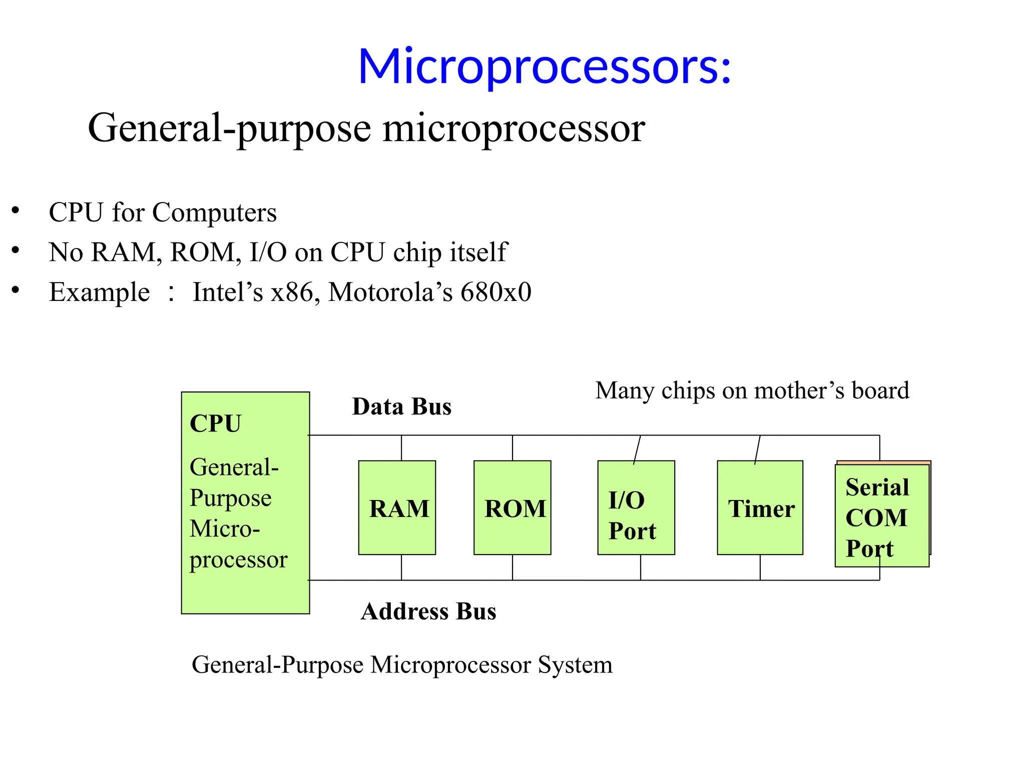
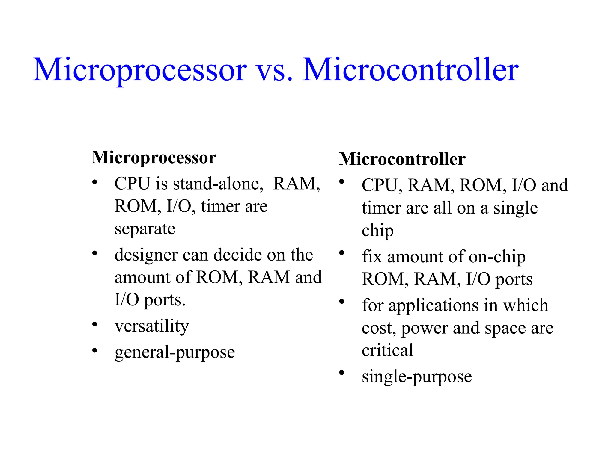
Microprocessor
• CPU isstand-alone, RAM,
ROM, I/O, timer are
separate
• designer can decide on the
amount of ROM, RAM and
I/O ports.
• versatility
• general-purpose
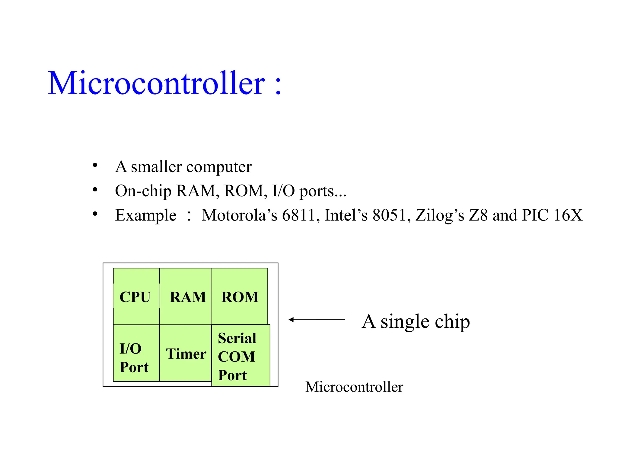
Microcontroller
• CPU, RAM, ROM, I/O and
timer are all on a single
chip
• fix amount of on-chip
ROM, RAM, I/O ports
• for applications in which
cost, power and space are
critical
• single-purpose
Microprocessor vs. Microcontroller
10.
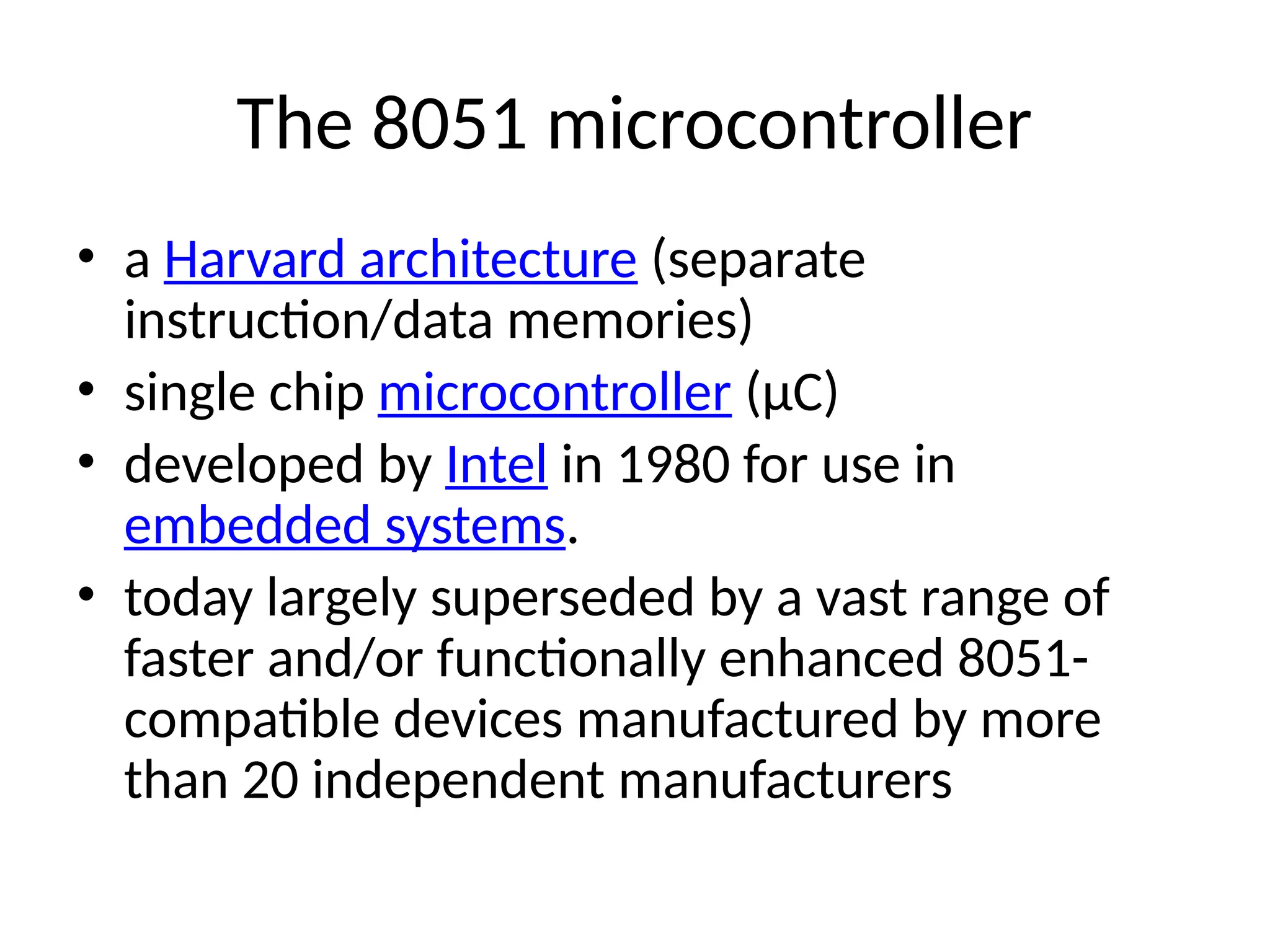
The 8051 microcontroller
•a Harvard architecture (separate
instruction/data memories)
• single chip microcontroller (µC)
• developed by Intel in 1980 for use in
embedded systems.
• today largely superseded by a vast range of
faster and/or functionally enhanced 8051-
compatible devices manufactured by more
than 20 independent manufacturers
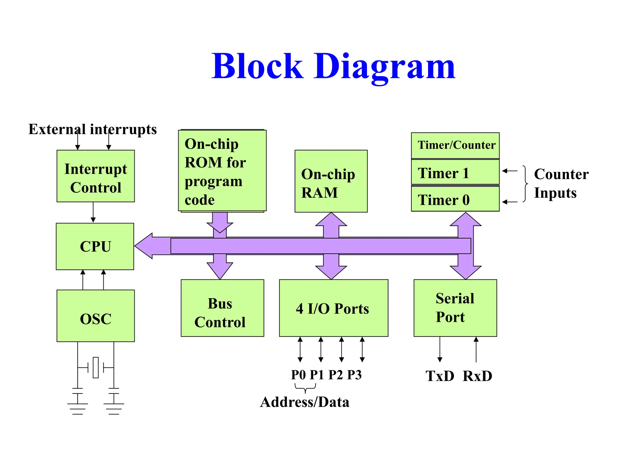
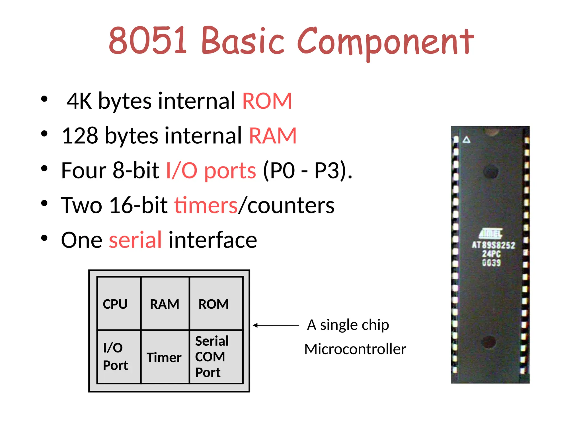
8051 Basic Component
•4K bytes internal ROM
• 128 bytes internal RAM
• Four 8-bit I/O ports (P0 - P3).
• Two 16-bit timers/counters
• One serial interface
RAM
I/O
Port
Timer
Serial
COM
Port
Microcontroller
CPU
A single chip
ROM
13.
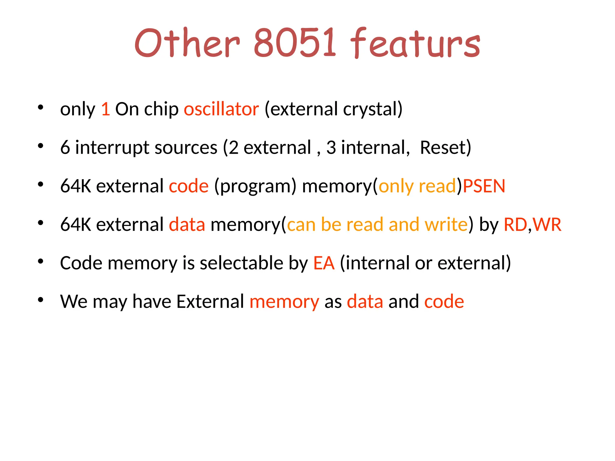
Other 8051 featurs
•only 1 On chip oscillator (external crystal)
• 6 interrupt sources (2 external , 3 internal, Reset)
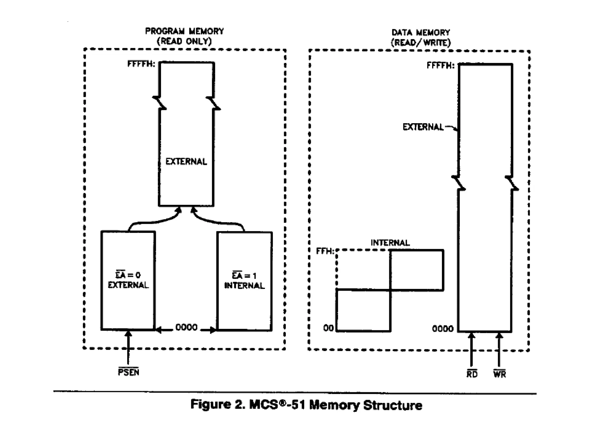
• 64K external code (program) memory(only read)PSEN
• 64K external data memory(can be read and write) by RD,WR
• Code memory is selectable by EA (internal or external)
• We may have External memory as data and code
14.
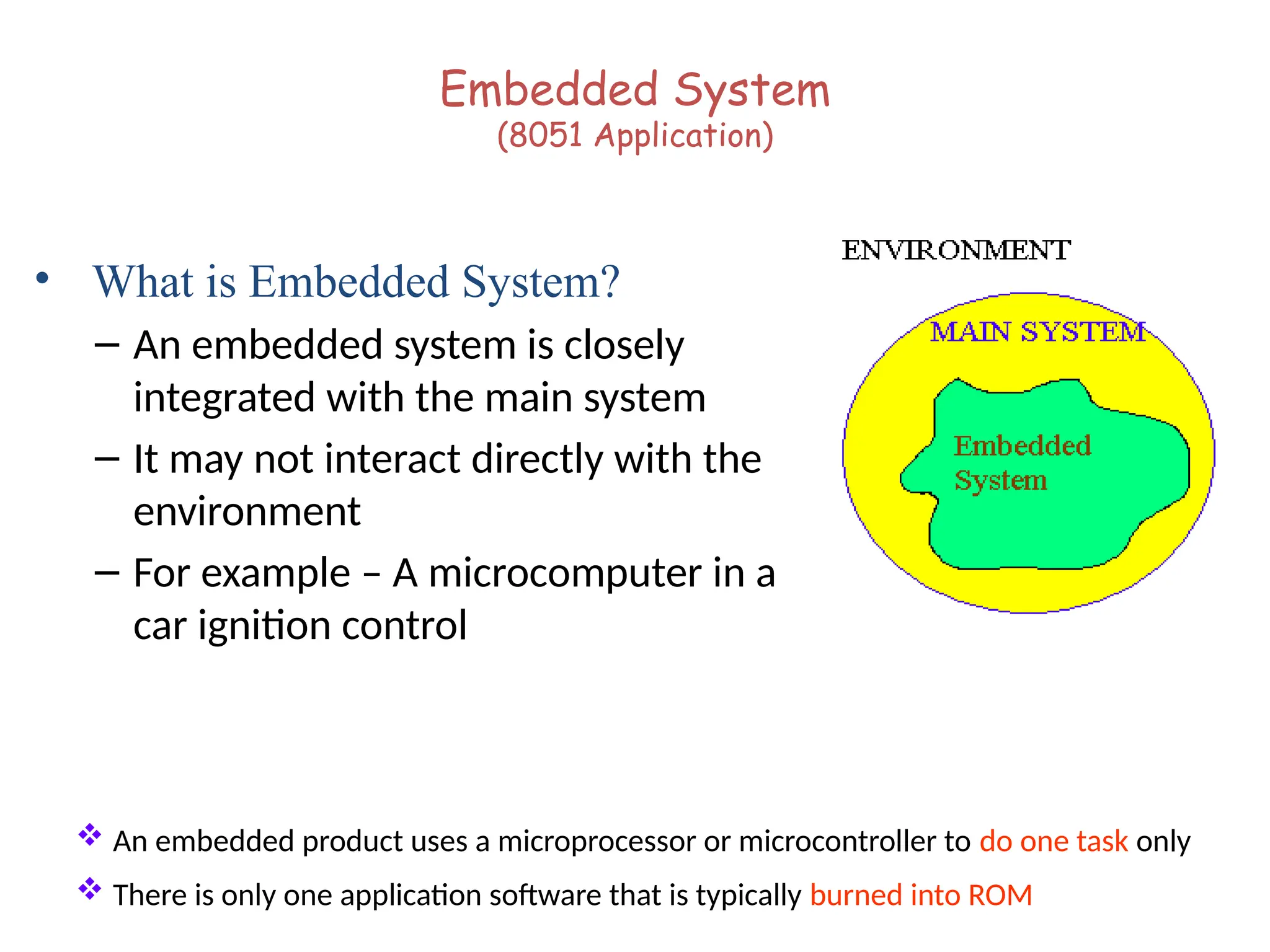
Embedded System
(8051 Application)
•What is Embedded System?
– An embedded system is closely
integrated with the main system
– It may not interact directly with the
environment
– For example – A microcomputer in a
car ignition control
An embedded product uses a microprocessor or microcontroller to do one task only
There is only one application software that is typically burned into ROM
15.
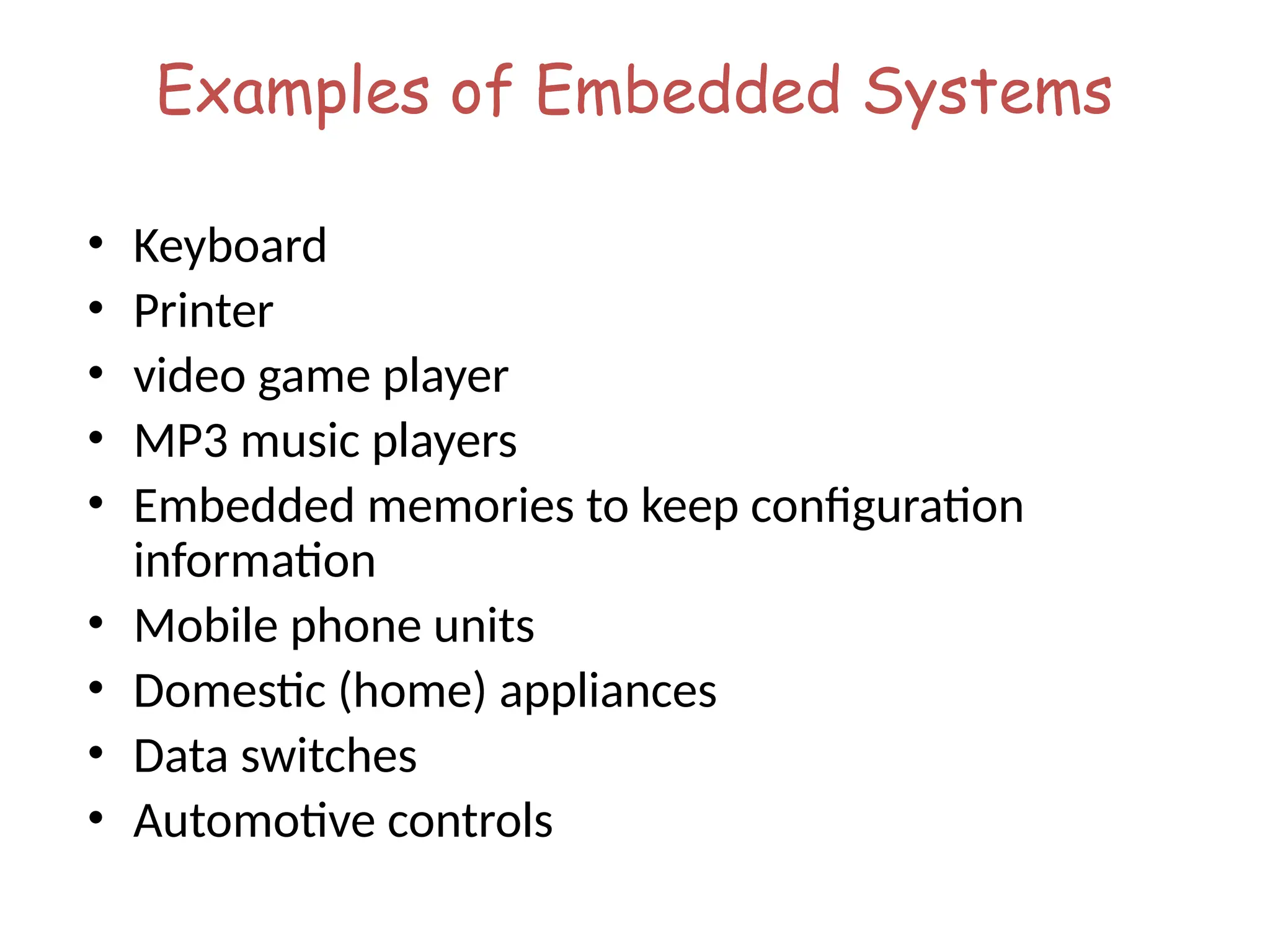
Examples of EmbeddedSystems
• Keyboard
• Printer
• video game player
• MP3 music players
• Embedded memories to keep configuration
information
• Mobile phone units
• Domestic (home) appliances
• Data switches
• Automotive controls
16.
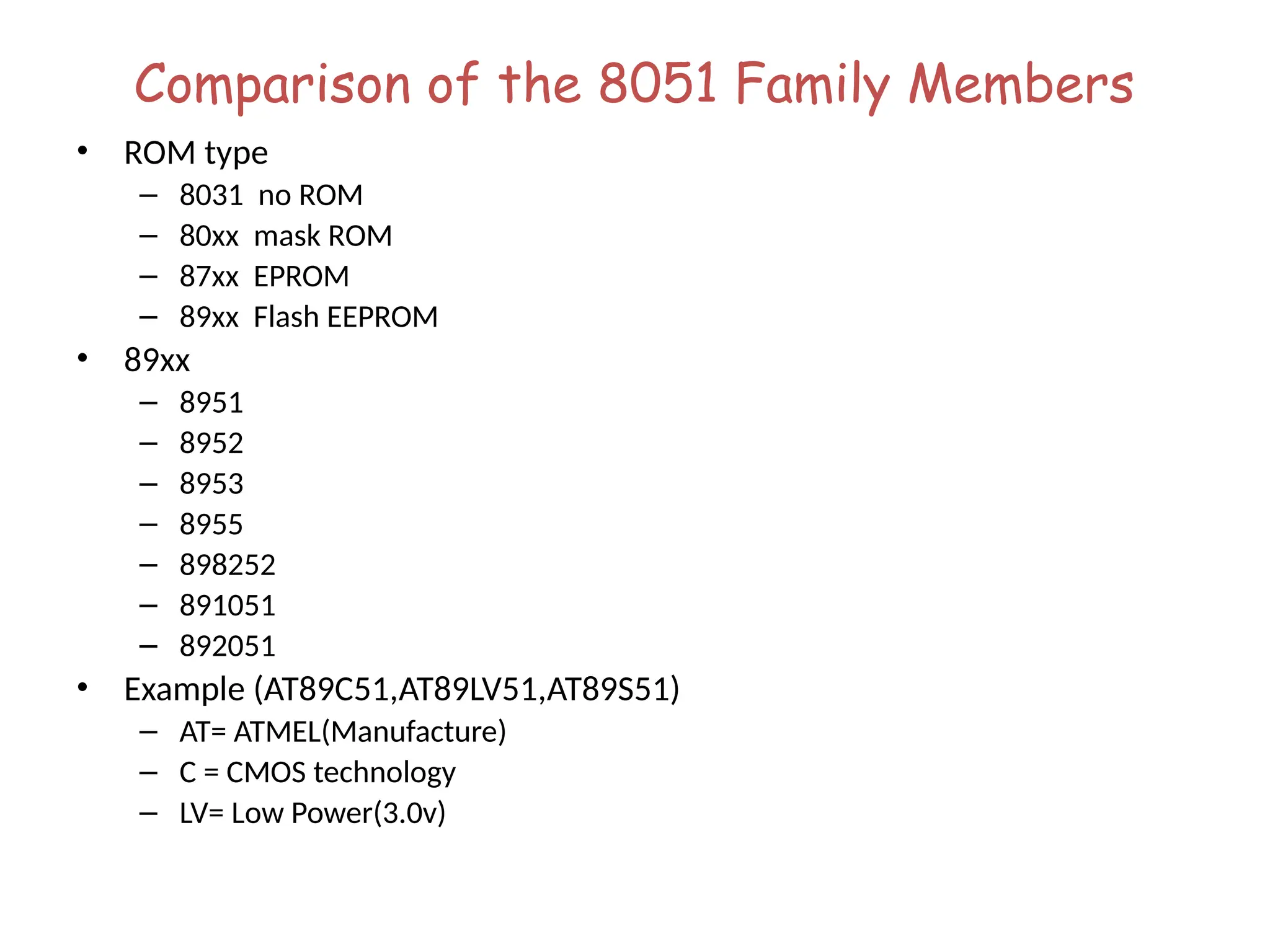
Comparison of the8051 Family Members
• ROM type
– 8031 no ROM
– 80xx mask ROM
– 87xx EPROM
– 89xx Flash EEPROM
• 89xx
– 8951
– 8952
– 8953
– 8955
– 898252
– 891051
– 892051
• Example (AT89C51,AT89LV51,AT89S51)
– AT= ATMEL(Manufacture)
– C = CMOS technology
– LV= Low Power(3.0v)
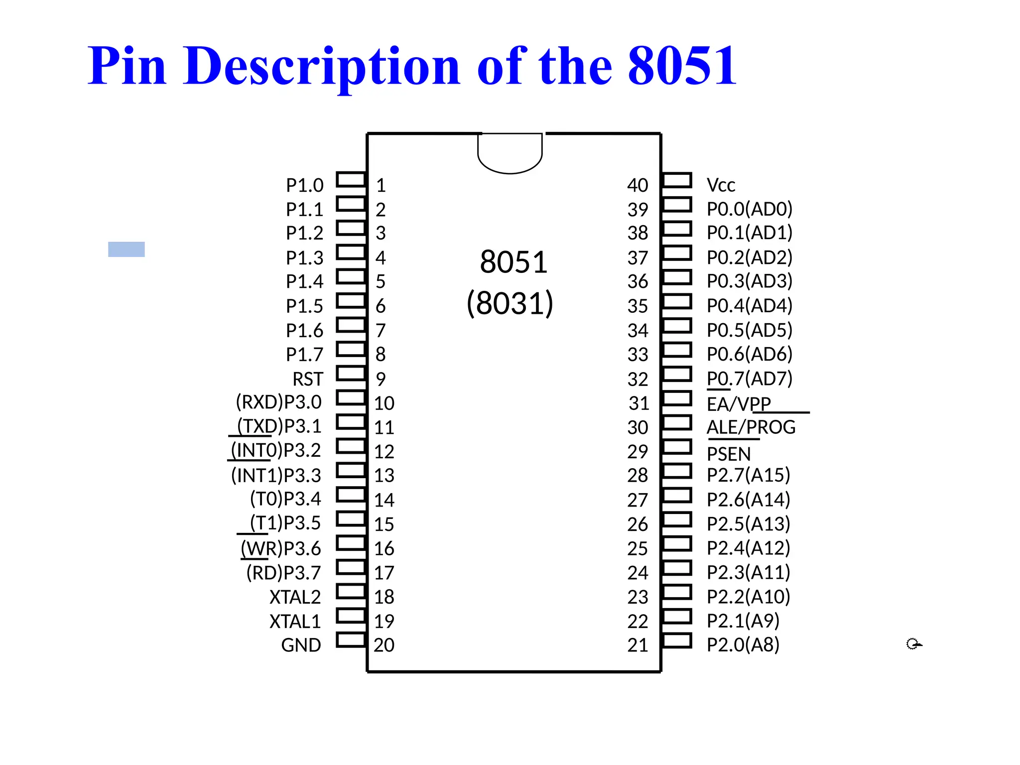
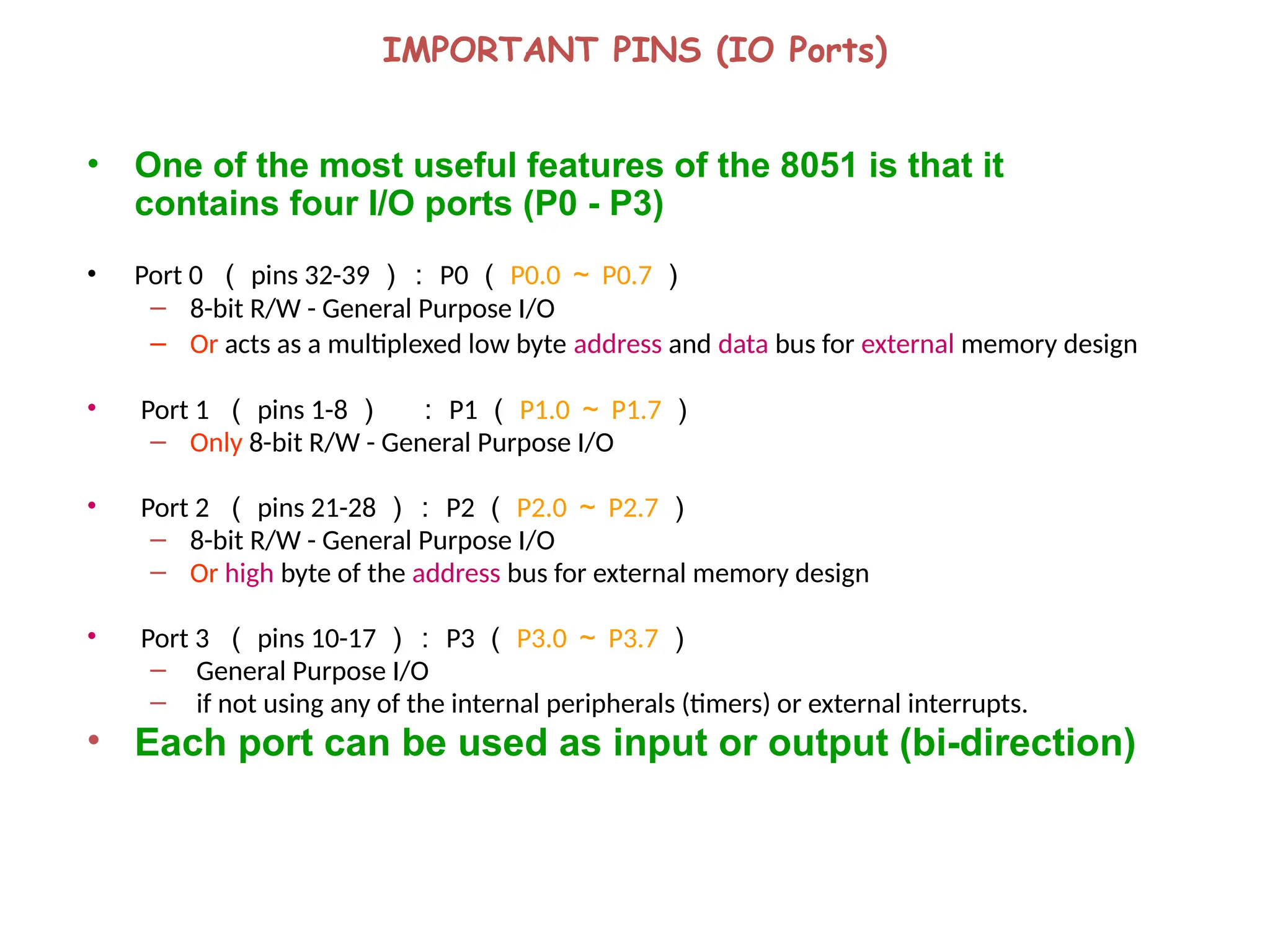
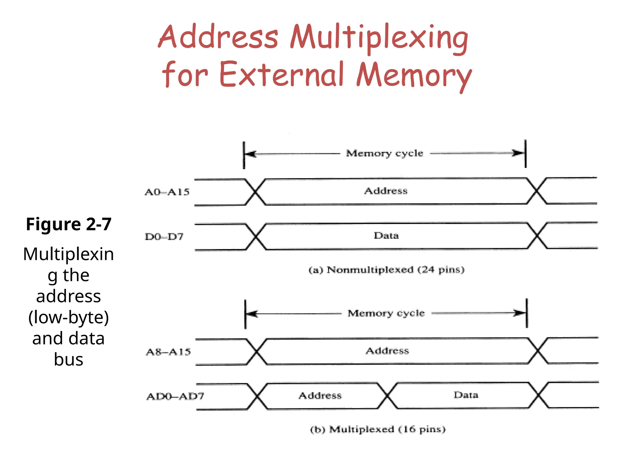
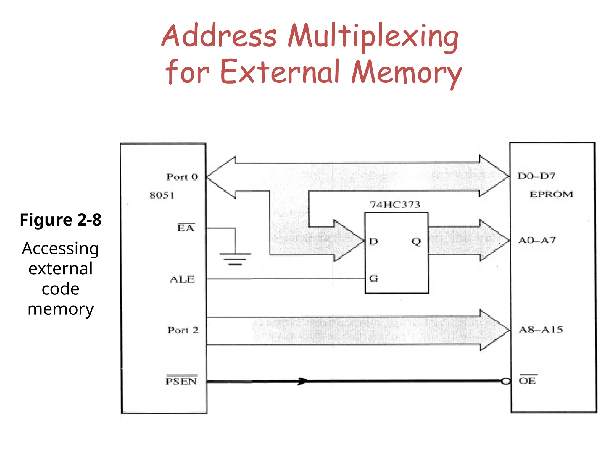
IMPORTANT PINS (IOPorts)
• One of the most useful features of the 8051 is that it
contains four I/O ports (P0 - P3)
• Port 0 ( pins 32-39 ): P0 ( P0.0 ~ P0.7 )
– 8-bit R/W - General Purpose I/O
– Or acts as a multiplexed low byte address and data bus for external memory design
• Port 1 ( pins 1-8 ) : P1 ( P1.0 ~ P1.7 )
– Only 8-bit R/W - General Purpose I/O
• Port 2 ( pins 21-28 ): P2 ( P2.0 ~ P2.7 )
– 8-bit R/W - General Purpose I/O
– Or high byte of the address bus for external memory design
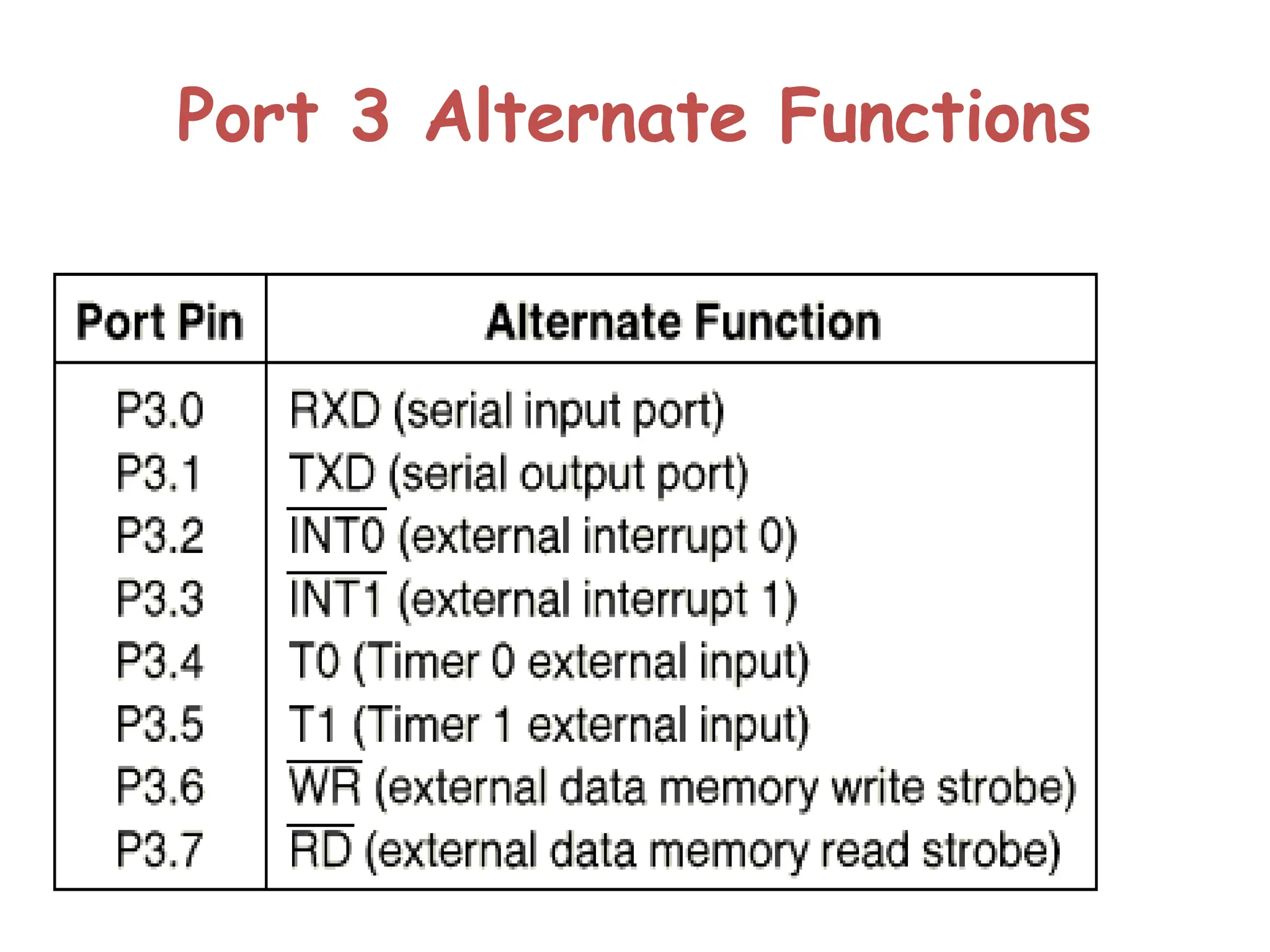
• Port 3 ( pins 10-17 ): P3 ( P3.0 ~ P3.7 )
– General Purpose I/O
– if not using any of the internal peripherals (timers) or external interrupts.
• Each port can be used as input or output (bi-direction)
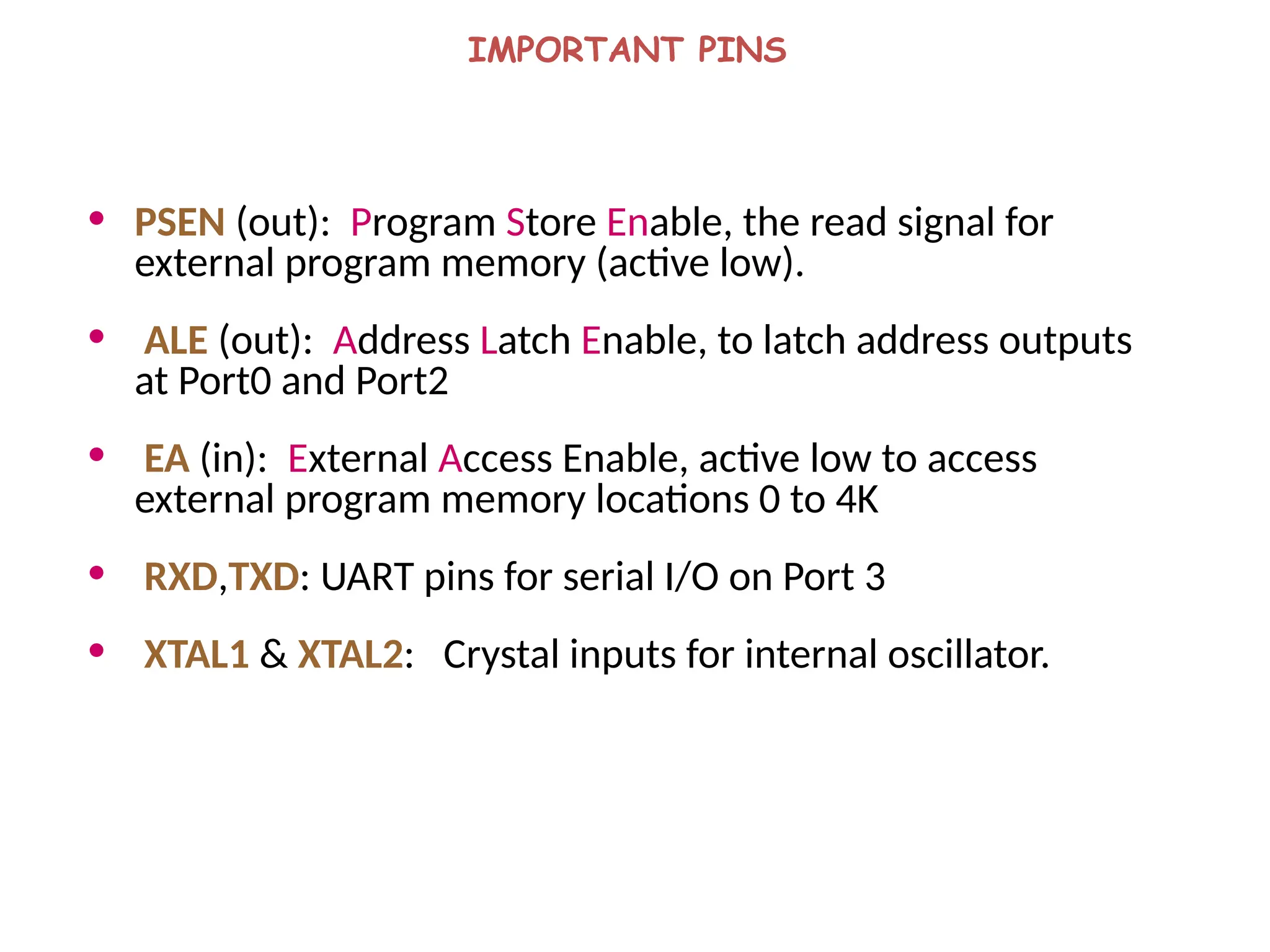
IMPORTANT PINS
• PSEN(out): Program Store Enable, the read signal for
external program memory (active low).
• ALE (out): Address Latch Enable, to latch address outputs
at Port0 and Port2
• EA (in): External Access Enable, active low to access
external program memory locations 0 to 4K
• RXD,TXD: UART pins for serial I/O on Port 3
• XTAL1 & XTAL2: Crystal inputs for internal oscillator.
21.
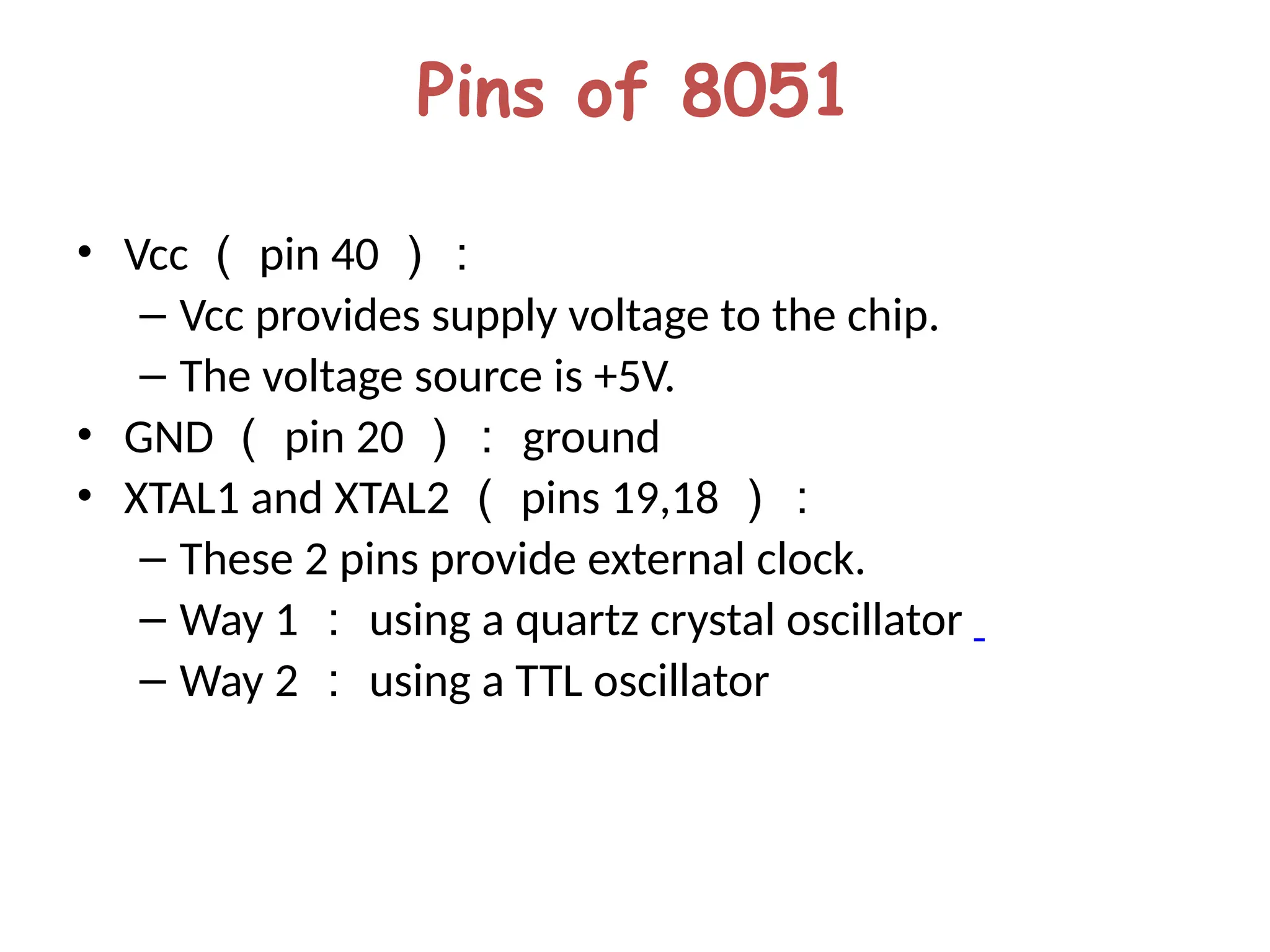
Pins of 8051
•Vcc ( pin 40 ):
– Vcc provides supply voltage to the chip.
– The voltage source is +5V.
• GND ( pin 20 ): ground
• XTAL1 and XTAL2 ( pins 19,18 ):
– These 2 pins provide external clock.
– Way 1 : using a quartz crystal oscillator
– Way 2 : using a TTL oscillator
22.
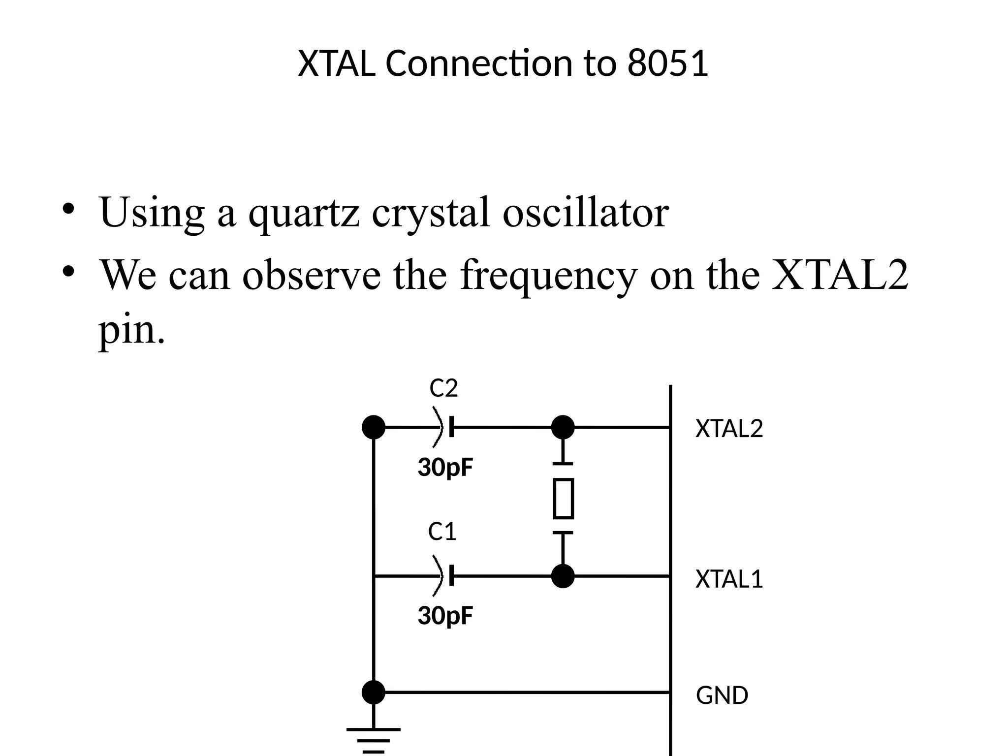
XTAL Connection to8051
• Using a quartz crystal oscillator
• We can observe the frequency on the XTAL2
pin.
C2
30pF
C1
30pF
XTAL2
XTAL1
GND
23.
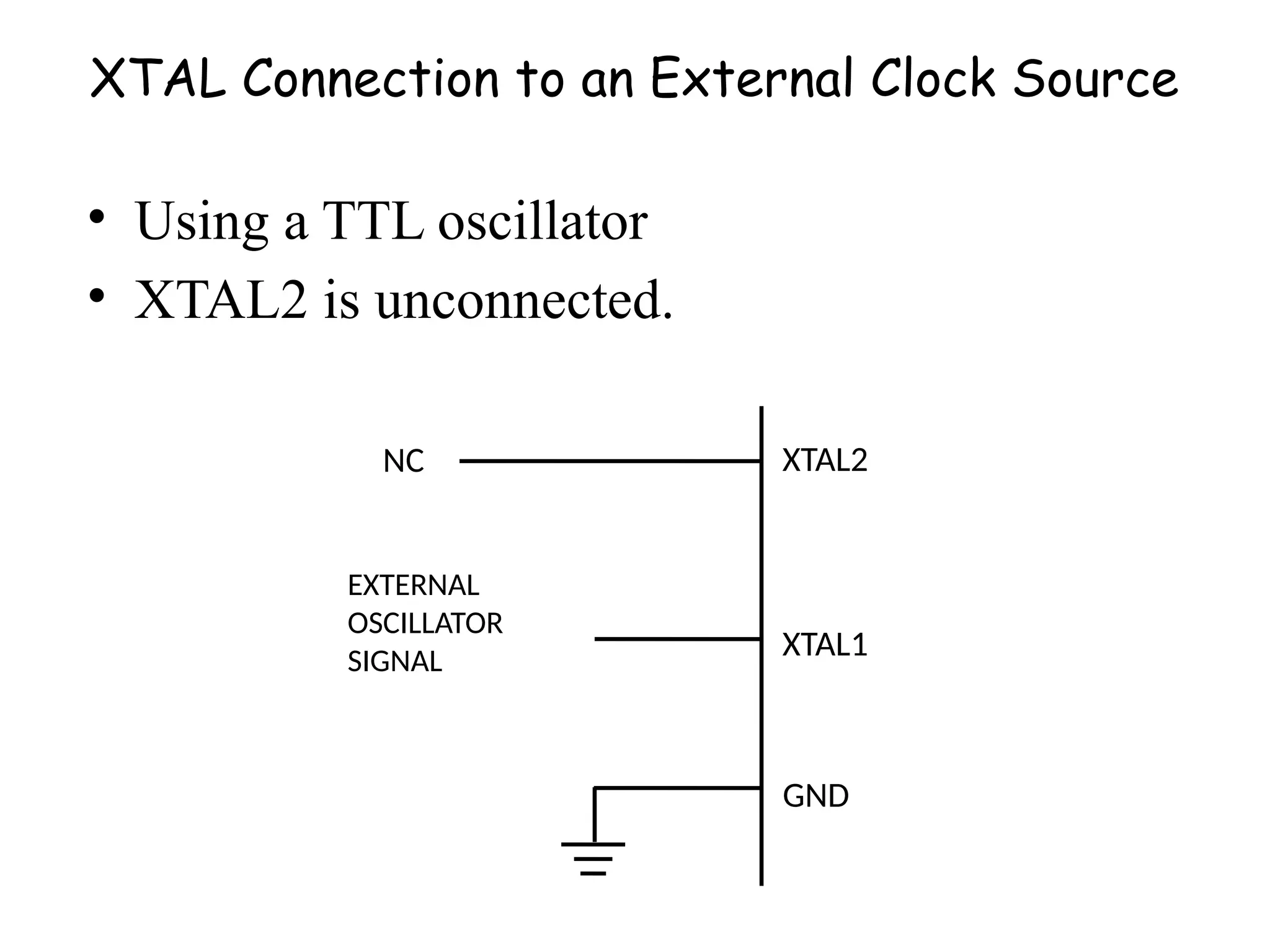
XTAL Connection toan External Clock Source
• Using a TTL oscillator
• XTAL2 is unconnected.
NC
EXTERNAL
OSCILLATOR
SIGNAL
XTAL2
XTAL1
GND
24.
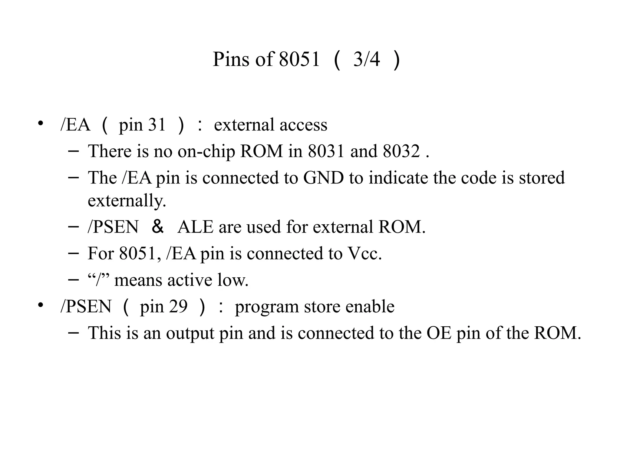
Pins of 8051( 3/4 )
• /EA ( pin 31 ): external access
– There is no on-chip ROM in 8031 and 8032 .
– The /EA pin is connected to GND to indicate the code is stored
externally.
– /PSEN & ALE are used for external ROM.
– For 8051, /EA pin is connected to Vcc.
– “/” means active low.
• /PSEN ( pin 29 ): program store enable
– This is an output pin and is connected to the OE pin of the ROM.
25.
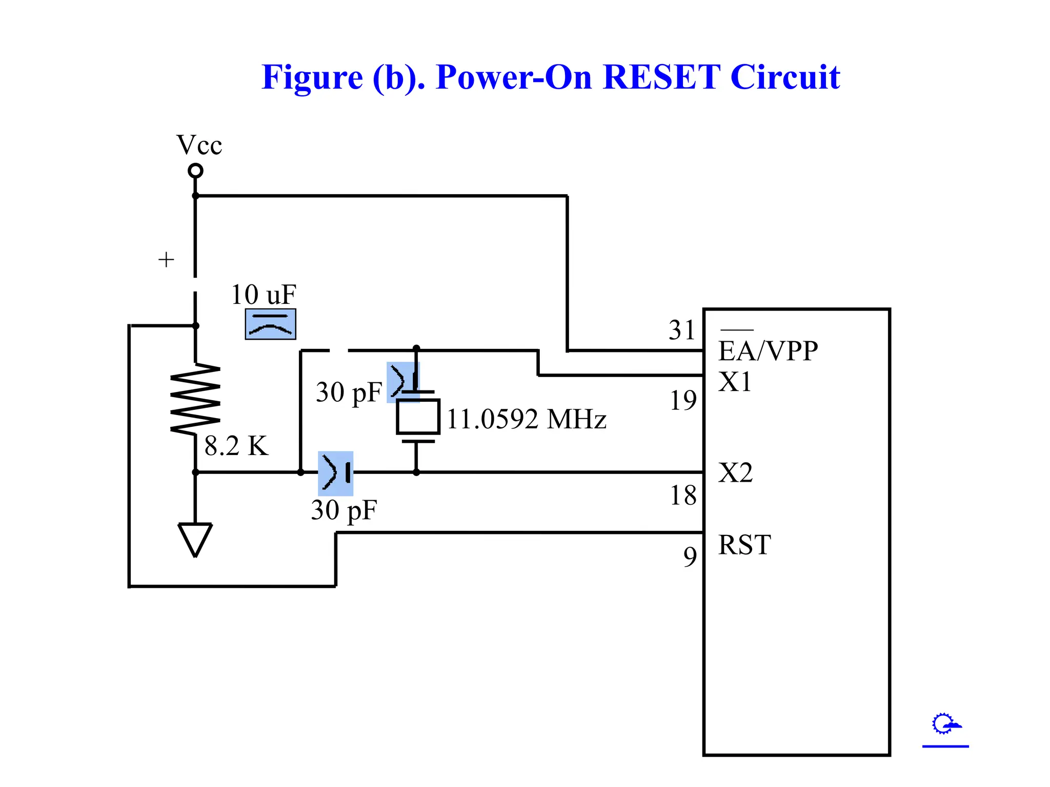
Pins of 8051
•RST ( pin 9 ): reset
– input pin and active high ( normally low ) .
• The high pulse must be high at least 2 machine
cycles.
– power-on reset.
• Upon applying a high pulse to RST, the
microcontroller will reset and all values in registers
will be lost.
• Reset values of some 8051 registers
– power-on reset circuit
26.
Pins of 8051
•RST ( pin 9 ): reset
– input pin and active high ( normally low ) .
• The high pulse must be high at least 2 machine
cycles.
– power-on reset.
• Upon applying a high pulse to RST, the
microcontroller will reset and all values in registers
will be lost.
• Reset values of some 8051 registers
– power-on reset circuit
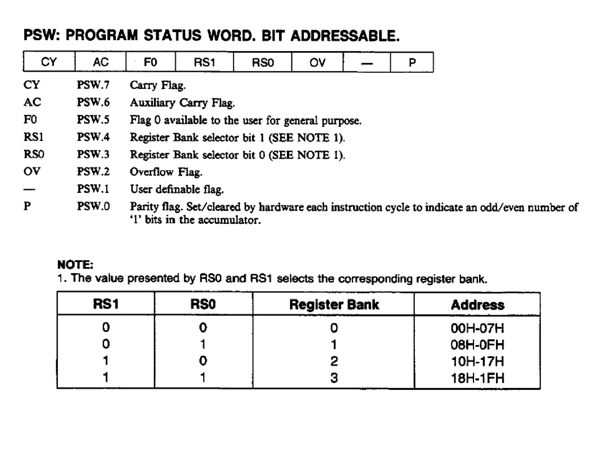
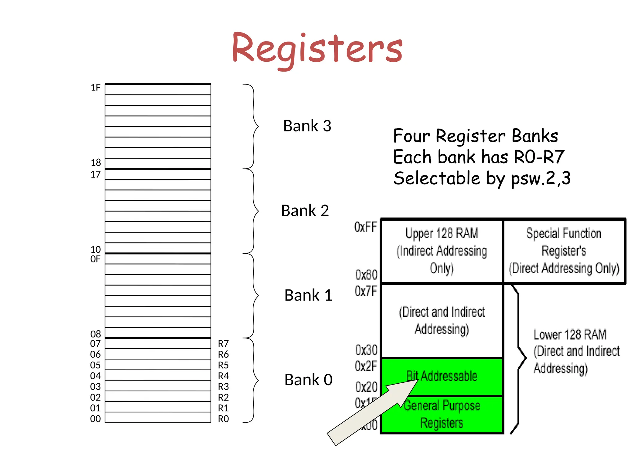
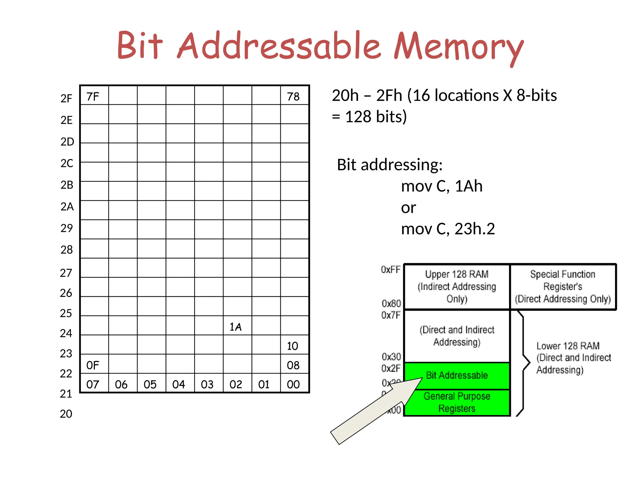
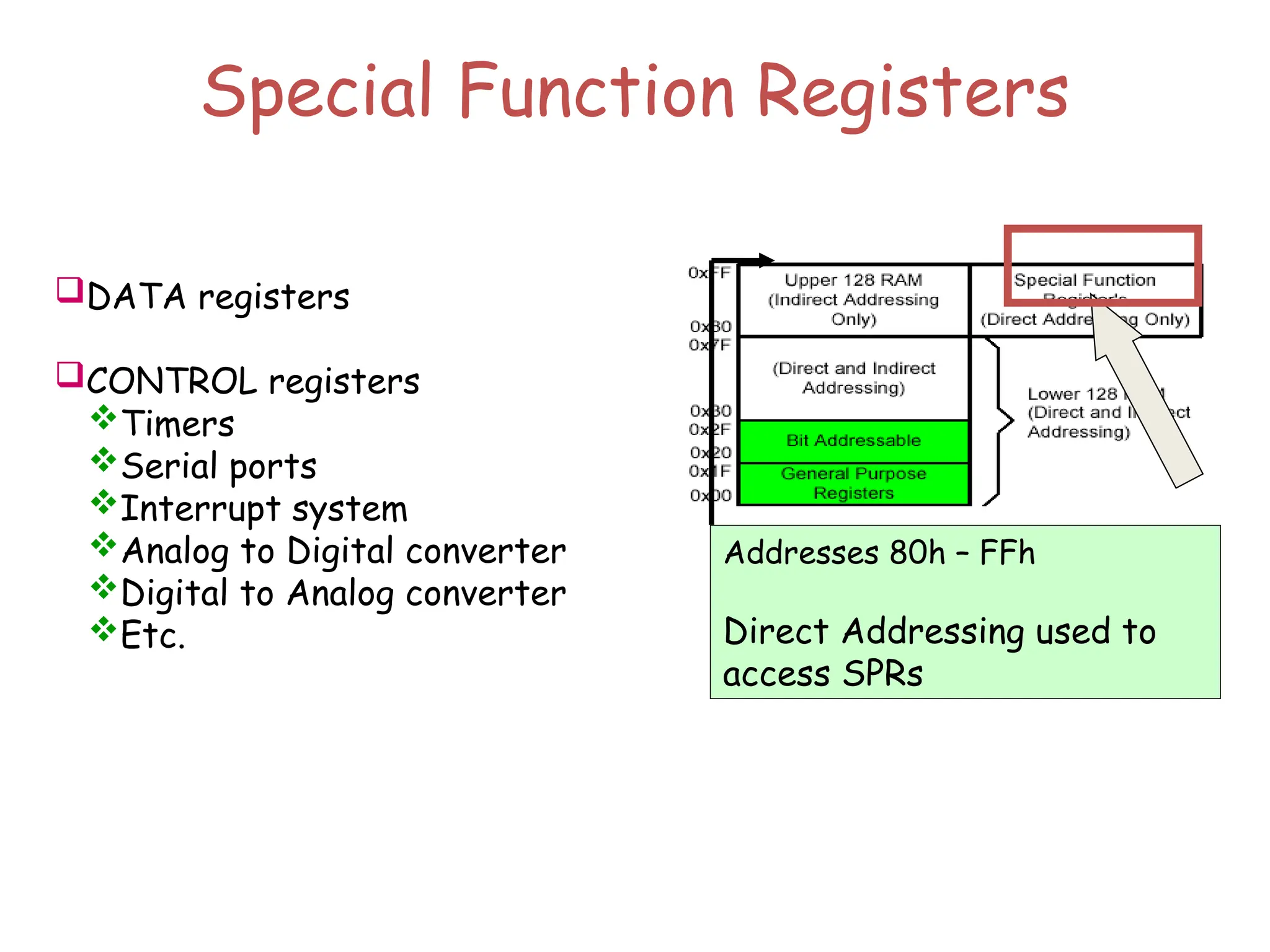
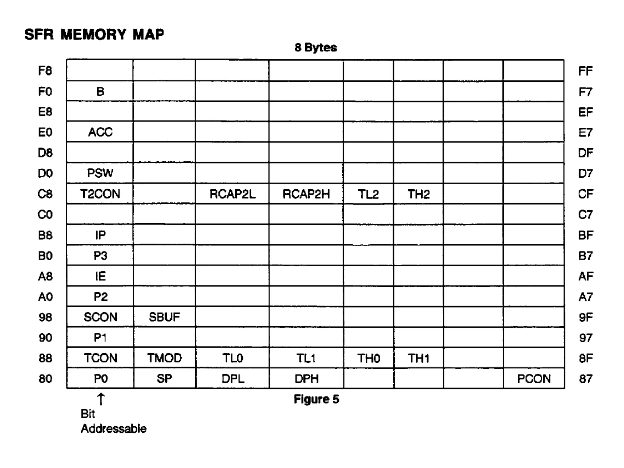
Special Function Registers
DATAregisters
CONTROL registers
Timers
Serial ports
Interrupt system
Analog to Digital converter
Digital to Analog converter
Etc.
Addresses 80h – FFh
Direct Addressing used to
access SPRs
35.
Active bankselected by PSW [RS1,RS0] bit
Permits fast “context switching” in interrupt
service routines (ISR).
Register Banks
Timers /Counters Programming
•The 8051 has 2 timers/counters: timer/counter 0 and
timer/counter 1. They can be used as
1. The timer is used as a time delay generator.
– The clock source is the internal crystal frequency of the 8051.
2. An event counter.
– External input from input pin to count the number of events on
registers.
– These clock pulses cold represent the number of people passing
through an entrance, or the number of wheel rotations, or any other
event that can be converted to pulses.
40.
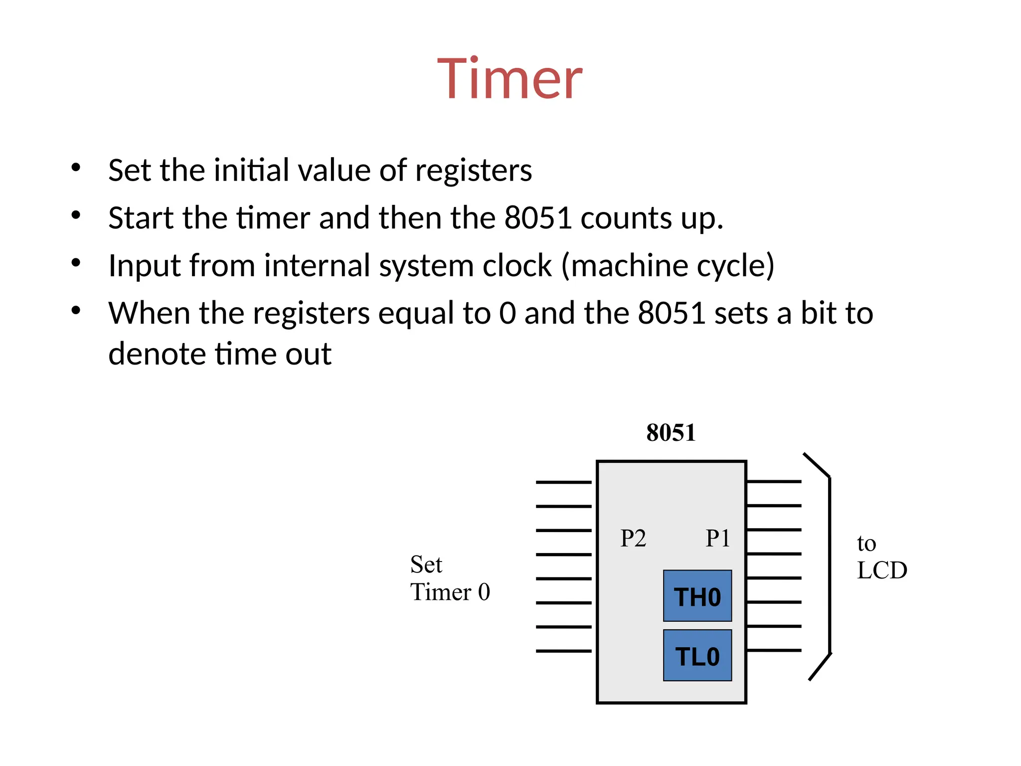
Timer
• Set theinitial value of registers
• Start the timer and then the 8051 counts up.
• Input from internal system clock (machine cycle)
• When the registers equal to 0 and the 8051 sets a bit to
denote time out
to
LCD
P1
8051
TL0
TH0
P2
Set
Timer 0
41.
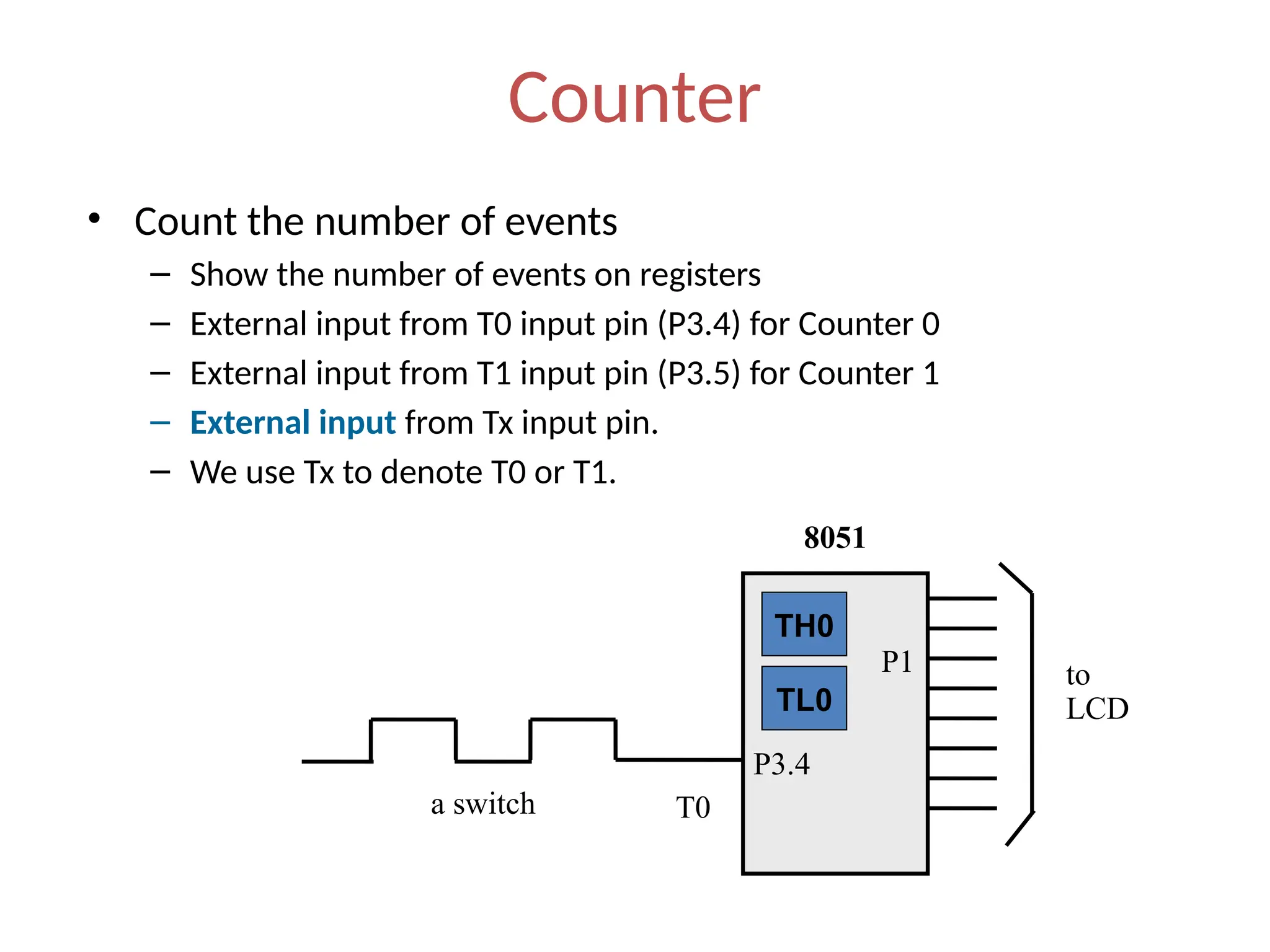
Counter
• Count thenumber of events
– Show the number of events on registers
– External input from T0 input pin (P3.4) for Counter 0
– External input from T1 input pin (P3.5) for Counter 1
– External input from Tx input pin.
– We use Tx to denote T0 or T1.
T0
to
LCD
P3.4
P1
8051
a switch
TL0
TH0
42.
Registers Used inTimer/Counter
• TH0, TL0, TH1, TL1
• TMOD (Timer mode register)
• TCON (Timer control register)
• Since 8052 has 3 timers/counters, the formats
of these control registers are different.
– T2CON (Timer 2 control register), TH2 and TL2 used
for 8052 only.
43.
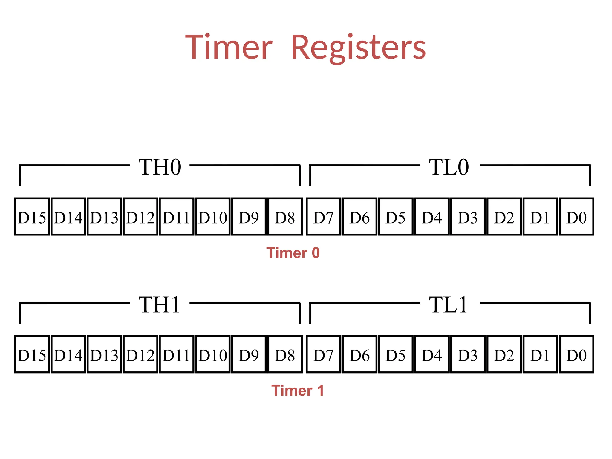
Basic Registers ofthe Timer
• Both timer 0 and timer 1 are 16 bits wide.
– These registers stores
• the time delay as a timer
• the number of events as a counter
– Timer 0: TH0 & TL0
• Timer 0 high byte, timer 0 low byte
– Timer 1: TH1 & TL1
• Timer 1 high byte, timer 1 low byte
– Each 16-bit timer can be accessed as two separate
registers of low byte and high byte.
44.
Basic Registers ofthe Timer
• Both timer 0 and timer 1 are 16 bits wide.
– These registers stores
• the time delay as a timer
• the number of events as a counter
– Timer 0: TH0 & TL0
• Timer 0 high byte, timer 0 low byte
– Timer 1: TH1 & TL1
• Timer 1 high byte, timer 1 low byte
– Each 16-bit timer can be accessed as two separate
registers of low byte and high byte.
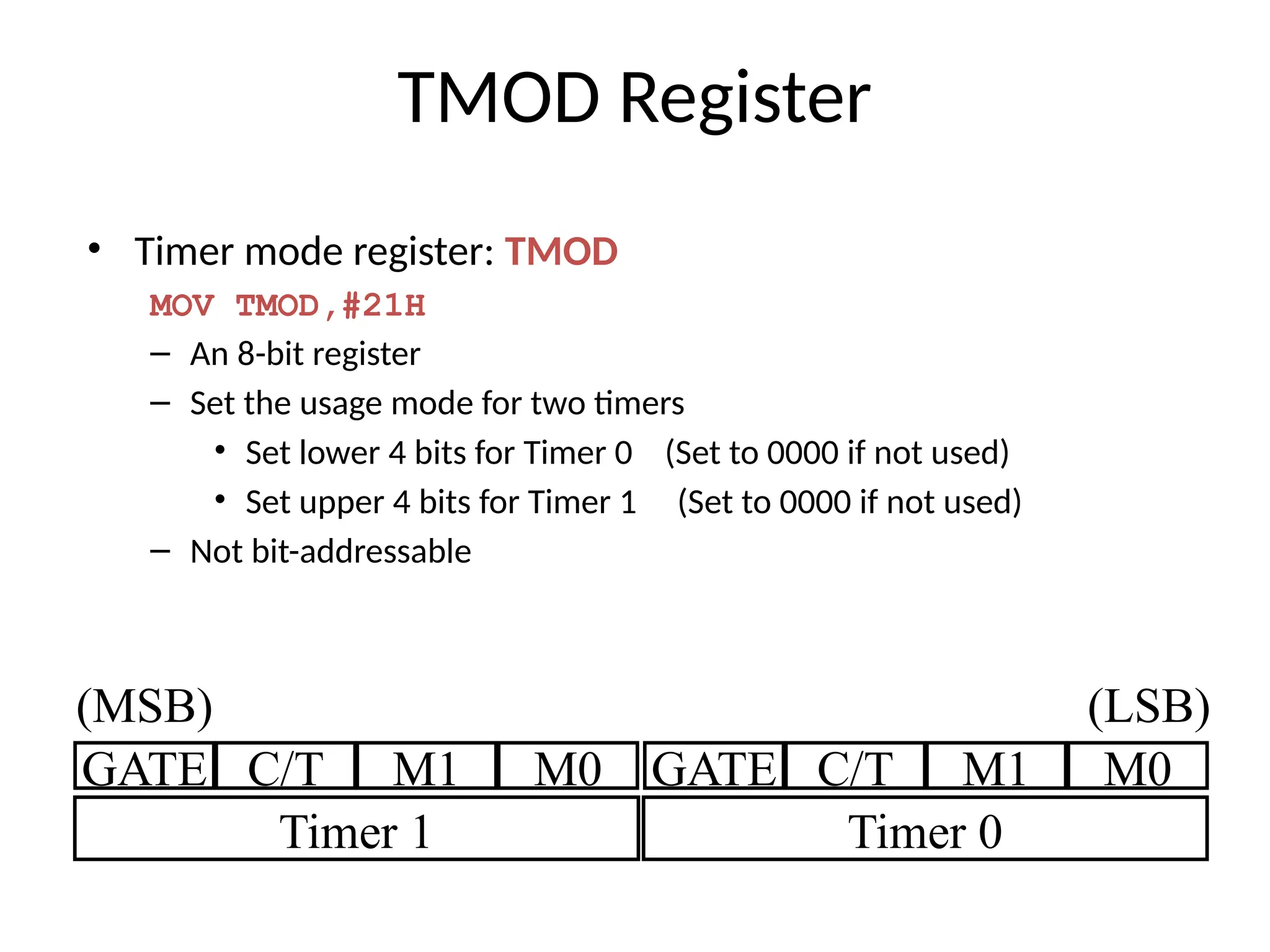
TMOD Register
• Timermode register: TMOD
MOV TMOD,#21H
– An 8-bit register
– Set the usage mode for two timers
• Set lower 4 bits for Timer 0 (Set to 0000 if not used)
• Set upper 4 bits for Timer 1 (Set to 0000 if not used)
– Not bit-addressable
GATE C/T M1 M0 GATE C/T M1 M0
Timer 1 Timer 0
(MSB) (LSB)
47.
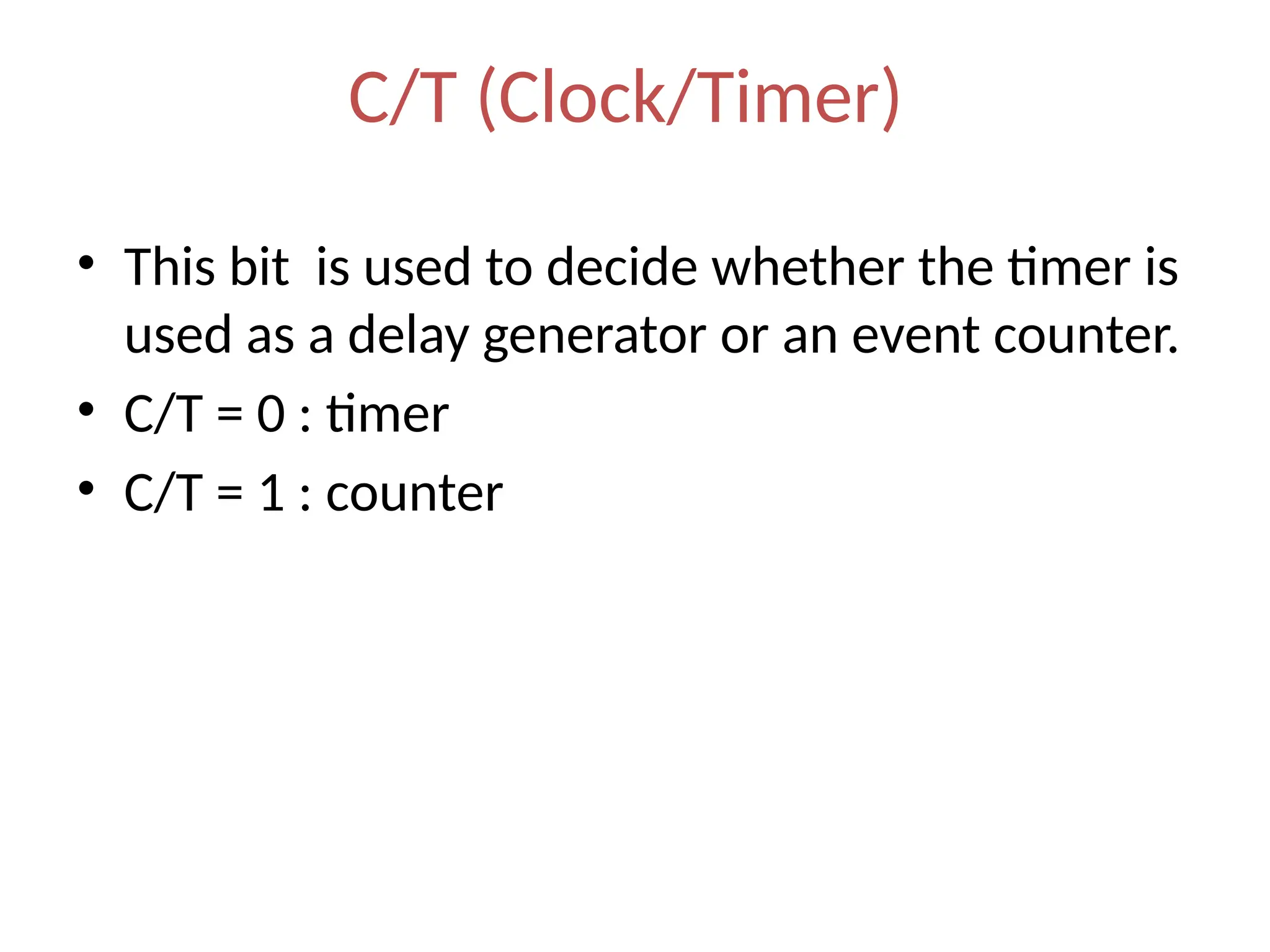
C/T (Clock/Timer)
• Thisbit is used to decide whether the timer is
used as a delay generator or an event counter.
• C/T = 0 : timer
• C/T = 1 : counter
48.
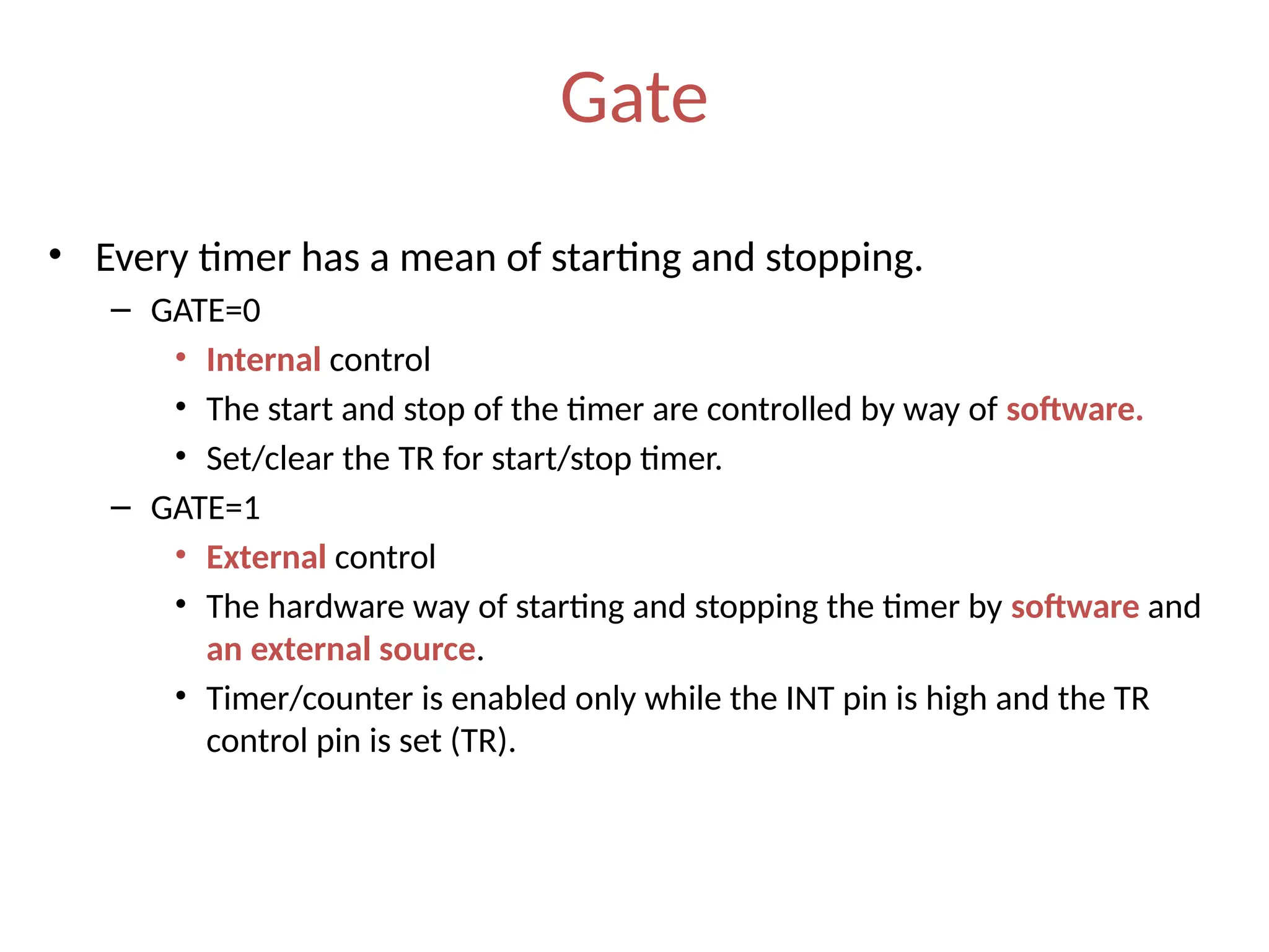
Gate
• Every timerhas a mean of starting and stopping.
– GATE=0
• Internal control
• The start and stop of the timer are controlled by way of software.
• Set/clear the TR for start/stop timer.
– GATE=1
• External control
• The hardware way of starting and stopping the timer by software and
an external source.
• Timer/counter is enabled only while the INT pin is high and the TR
control pin is set (TR).
49.
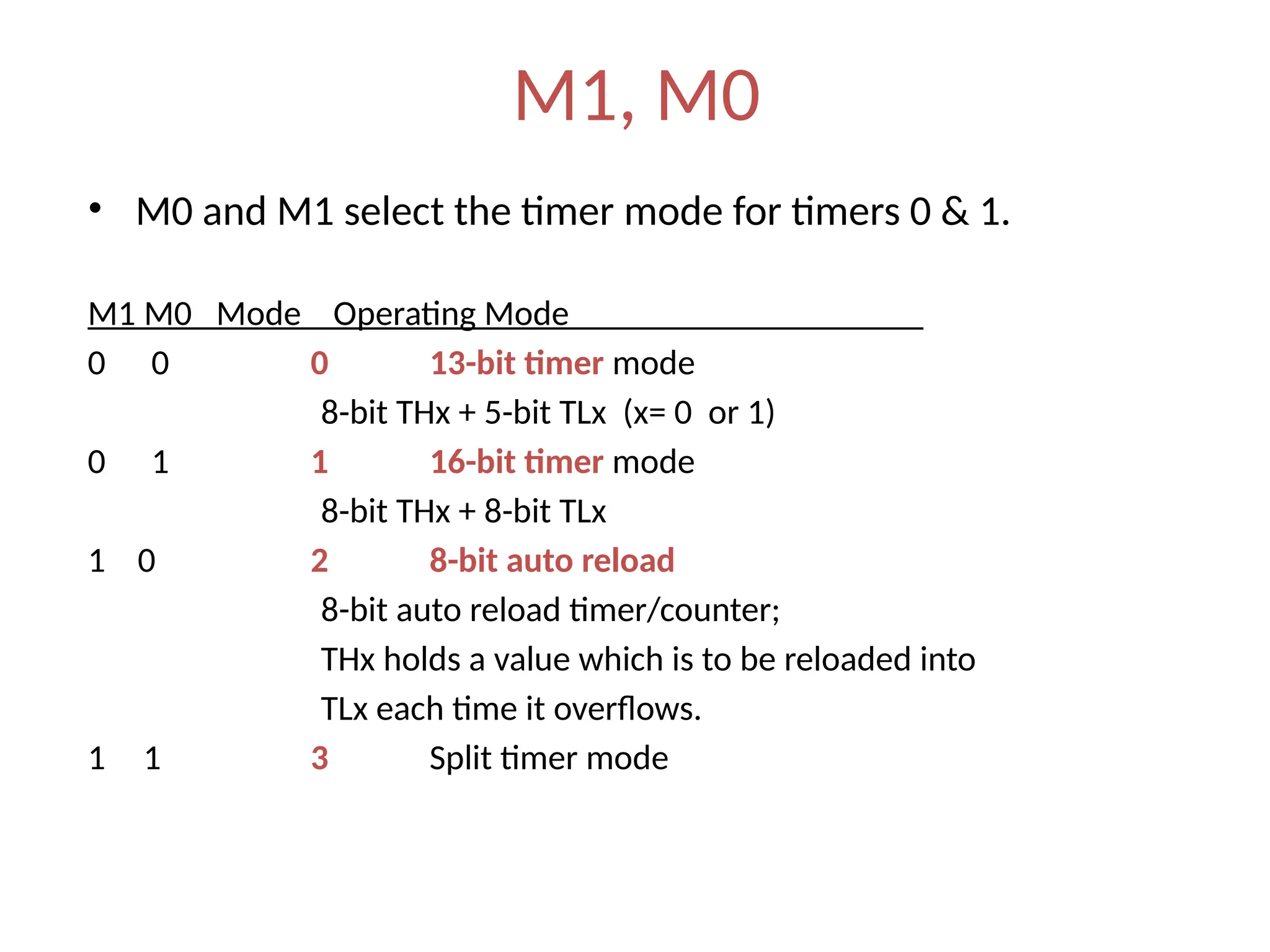
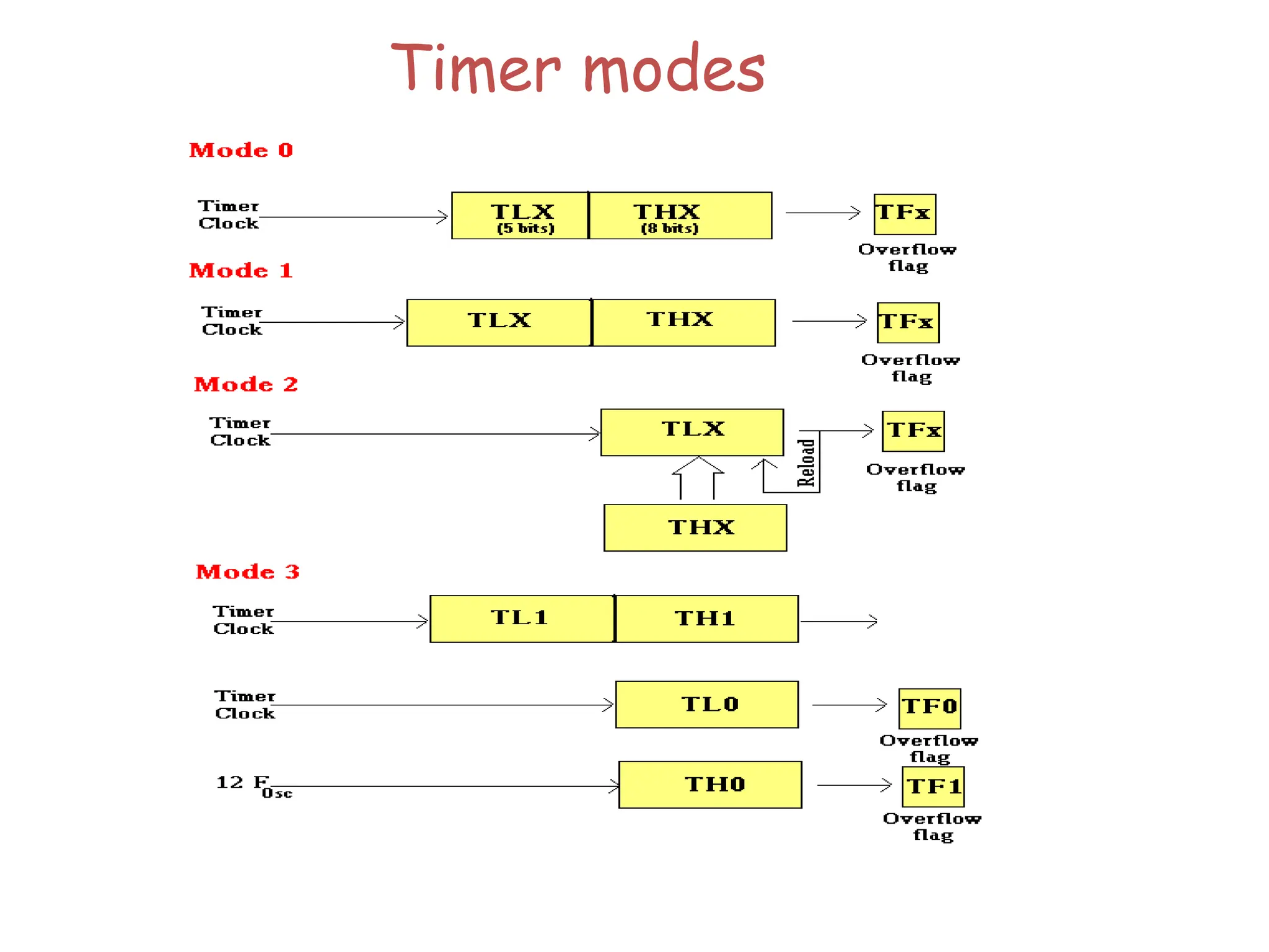
M1, M0
• M0and M1 select the timer mode for timers 0 & 1.
M1 M0 Mode Operating Mode
0 0 0 13-bit timer mode
8-bit THx + 5-bit TLx (x= 0 or 1)
0 1 1 16-bit timer mode
8-bit THx + 8-bit TLx
1 0 2 8-bit auto reload
8-bit auto reload timer/counter;
THx holds a value which is to be reloaded into
TLx each time it overflows.
1 1 3 Split timer mode
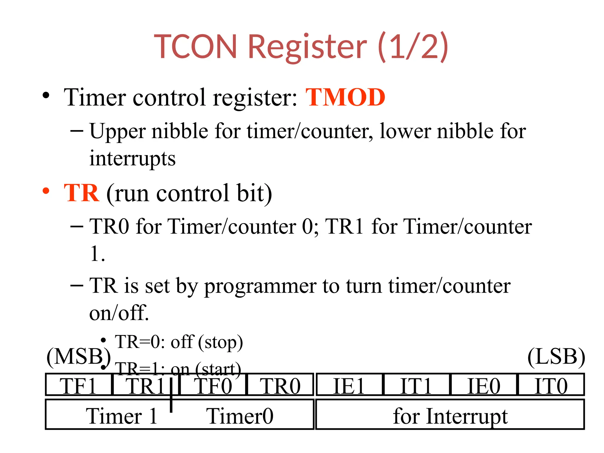
TCON Register (1/2)
•Timer control register: TMOD
– Upper nibble for timer/counter, lower nibble for
interrupts
• TR (run control bit)
– TR0 for Timer/counter 0; TR1 for Timer/counter
1.
– TR is set by programmer to turn timer/counter
on/off.
• TR=0: off (stop)
• TR=1: on (start)
TF1 TR1 TF0 TR0 IE1 IT1 IE0 IT0
Timer 1 Timer0 for Interrupt
(MSB) (LSB)
52.
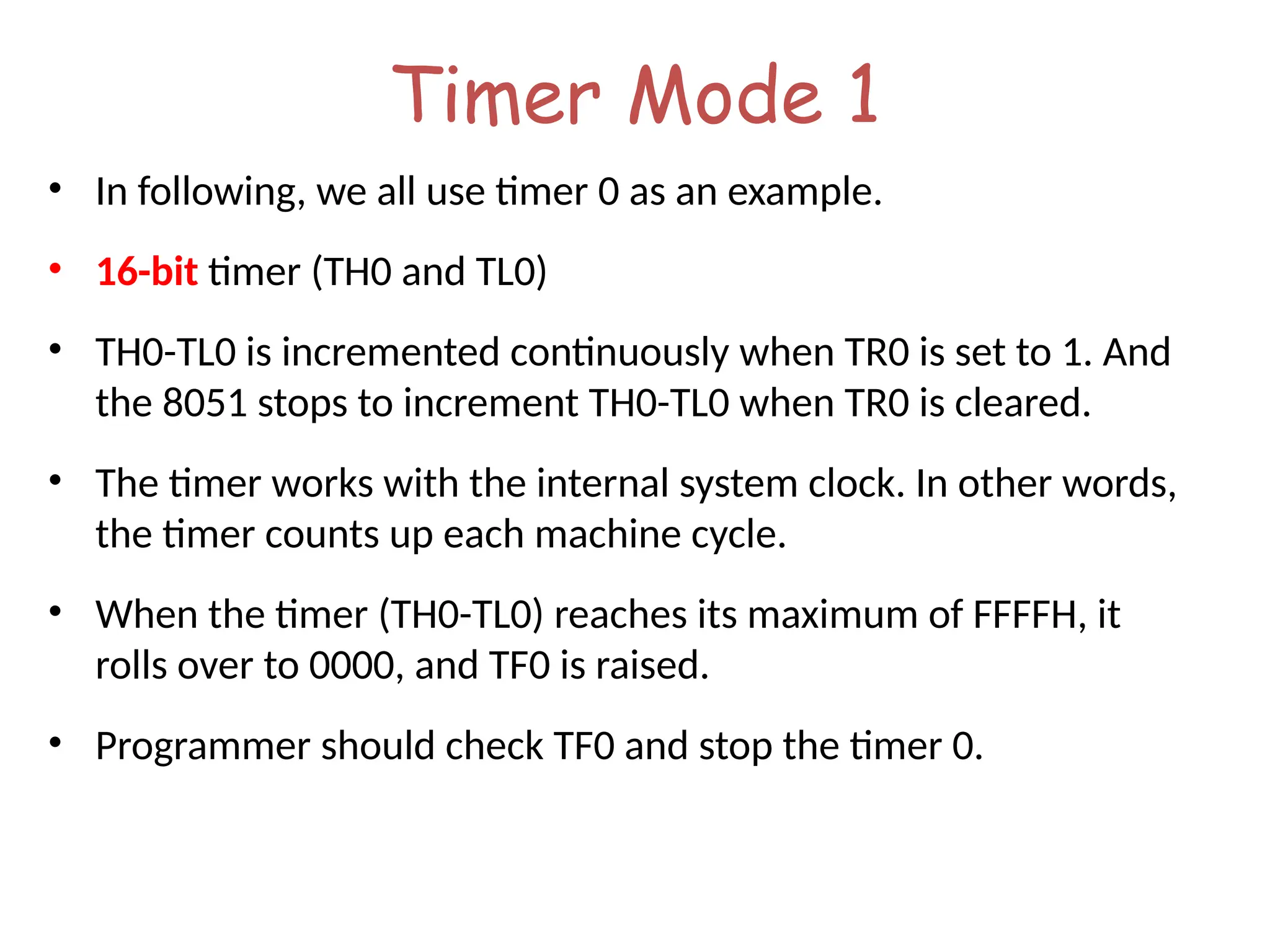
Timer Mode 1
•In following, we all use timer 0 as an example.
• 16-bit timer (TH0 and TL0)
• TH0-TL0 is incremented continuously when TR0 is set to 1. And
the 8051 stops to increment TH0-TL0 when TR0 is cleared.
• The timer works with the internal system clock. In other words,
the timer counts up each machine cycle.
• When the timer (TH0-TL0) reaches its maximum of FFFFH, it
rolls over to 0000, and TF0 is raised.
• Programmer should check TF0 and stop the timer 0.

![ Active bank selected by PSW [RS1,RS0] bit
Permits fast “context switching” in interrupt
service routines (ISR).
Register Banks](https://image.slidesharecdn.com/unit2and3rdppt-1-250419071521-d2ae02bb/75/Unit-two-and-unit-three-pptx-for-btech-ece-35-2048.jpg)