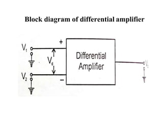
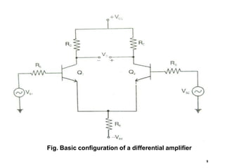
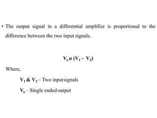
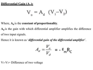
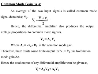
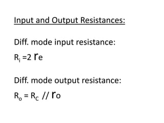
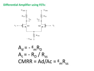
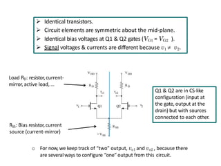
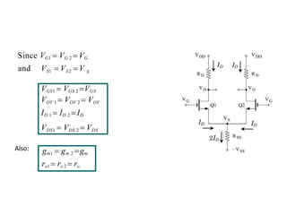
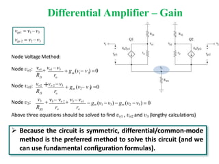
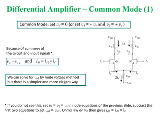
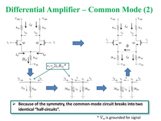
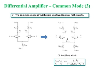
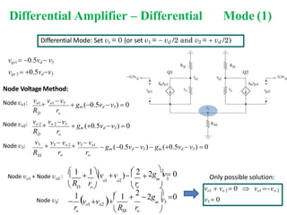
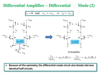
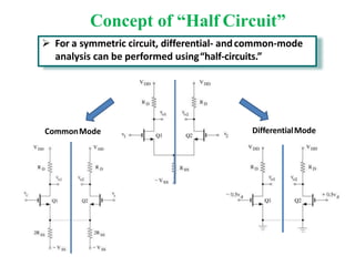
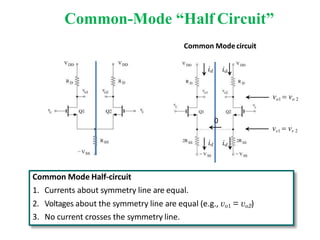
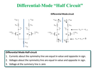
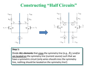
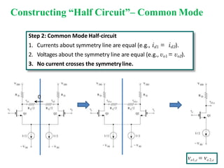
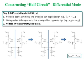
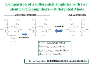
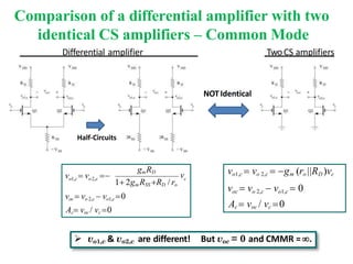
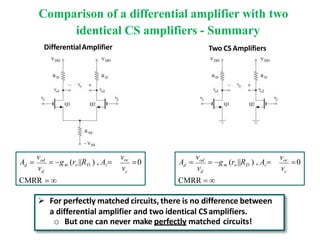
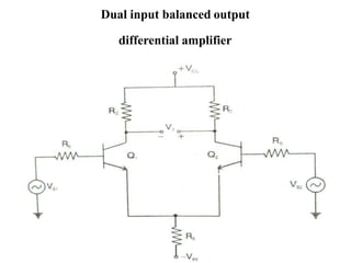
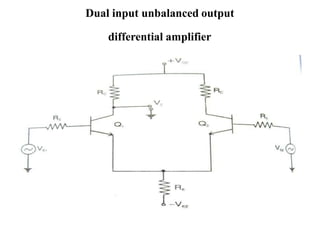
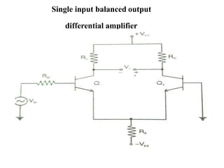
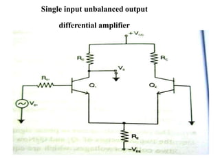
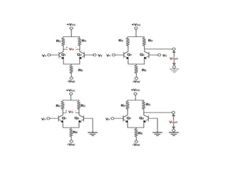
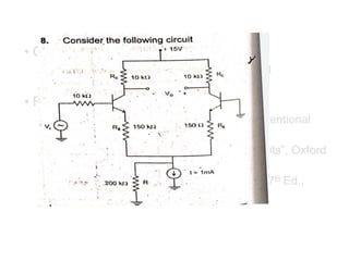
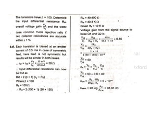
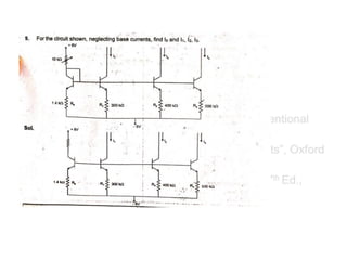
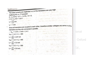
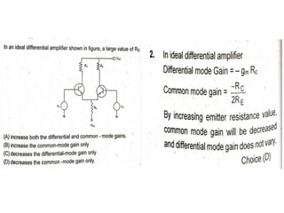
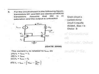
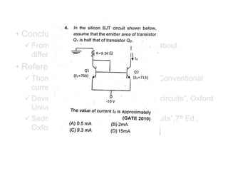
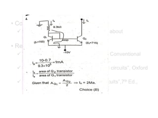
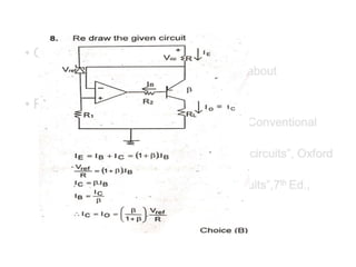
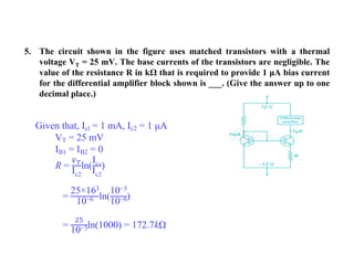
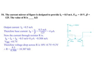
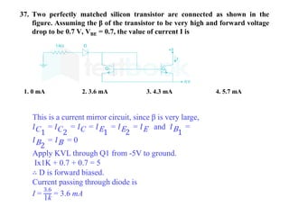
SlideShare a Scribd company logo
1 of 62
Download to read offline
Analog Circuits
Day-10
Differential Amplifiers
Introduction
• The function of differential amplifier is to amplify the
difference of two signals.
• The need for differential amplifier in many physical
measurements arises where response from d.c to many
megahertz is required. It is also the basic input stage of an
integrated amplifier.
Block diagram of differential amplifier
9
Fig. Basic configuration of a differential amplifier
• The output signal in a differential amplifier is proportional to the
difference between the two input signals.
Vo α (V1 – V2)
Where,
V1 & V2 – Two inputsignals
Vo – Single ended output
Differential Gain (Ad):
Where, Ad is the constant of proportionality.
Ad is the gain with which differential amplifier amplifies the difference
of two input signals.
Hence it is known as ‘differential gain of the differential amplifier’.
V1-V2= Difference of two voltage
= - g
mRC
Common Mode Gain (Ad):
An average of the two input signals is called common mode
signal denoted as Vc.
Hence, the differential amplifier also produces the output
voltage proportional to common mode signals.
Vo = Ac Vc
Where Ac = - RC / RE , is the common modegain.
Therefore, there exists some finite output for V1 = V2 due to common
mode gainAc.
Hence the total output of any differential amplifier can be given as,
Vo= Ad Vd + AcVc
Common Mode Rejection Ratio (CMRR):
• The ability of a differential amplifier to reject a common mode signal is
defined by a ratio called ‘Common Mode Rejection Ratio’ denoted as
CMRR.
• CMRR is defined as the ratio of the differential voltage gain Ad to
common mode gain Ac and is expresses indB.
CMRR = Ad/Ac = g
mRE
Input and Output Resistances:
Diff. mode input resistance:
Ri =2 re
Diff. mode output resistance:
Ro = RC // ro
Differential Amplifier using FETs:
Ad = - g
mRD
Ac = - RD / Rss
CMRR = Ad/Ac = g
mRss
 Identical transistors.
 Circuit elements are symmetric about the mid-plane.
 Identical bias voltages at Q1 & Q2 gates (VG1 = VG2 ).
 Signal voltages & currents are different because v1  v2.
Load RD: resistor,current-
mirror, active load, …
RSS: Bias resistor,current
source (current-mirror)
o For now, we keep track of “two” output, vo1 and vo2 , because there
are several ways to configure “one” output from this circuit.
Q1 & Q2 are in CS-like
configuration (input at
the gate, output at the
drain) but with sources
connected to each other.
ID ID
ID
ID
2ID
VGS1  VGS 2 VGS
VOV 1  VOV 2  VOV
ID 1  ID 2 ID
VDS1  VDS 2  VDS
S
S1 S2
and V  V V
Since VG1  VG 2  VG
gm1  gm 2 gm
ro1  ro 2  ro
Also:
Differential Amplifier – Gain
v3
r
R
 g (v  v ) 0
R r
 gm (v1  v3)  gm (v2 v3)  0
 v3  vo 2  v3  vo1
SS
R ro ro
m 2 3
 g (v  v ) 0
o
vo 2 v3
D
m 1 3
D o
vo1  vo1 v3
Node Voltage Method:
Node vo1:
Node vo2: vo2
Node v3:
Above three equations should be solved to find vo1 , vo2 and v3 (lengthy calculations)
vgs1  v1 v3
vgs 2  v2 v3
 Because the circuit is symmetric, differential/common-mode
method is the preferred method to solve this circuit (and we
can use fundamental configuration formulas).
Differential Amplifier – Common Mode (1)
Because of summery of
the circuit and input signals*:
Common Mode: Set vd = 0 (or set v1 =  vc and v2 =  vc )
vo1 vo 2 and id1  id 2 id
We can solve for vo1 by node voltage method
but there is a simpler and more elegant way.
id
id
id
2id
* If you do not see this, set v1 = v2 = vc in node equations of the previous slide, subtract the
first two equations to get vo1 = vo2 . Ohm’s law on RD then gives id1 = id2 =id
Differential Amplifier – Common Mode (2)
 Because of the symmetry, the common-mode circuit breaks into two
identical “half-circuits”.
id
id
id
2id
id
0
id
v3  2id RSS *
* Vss is grounded for signal
Differential Amplifier – Common Mode (3)
gm RD
1 2gm RSS RD / ro
vo1 vo 2 
vc vc
CS Amplifiers withRs
0
 The common-mode circuit breaks into two identical half-circuits.
Differential Amplifier – Differential Mode (1)
R
v3
r
R
R r
 gm (0.5vd v3)  gm (0.5vd  v3)  0
ro ro
 v3  vo 2  v3  vo1
SS
 gm (0.5vd v3)  0
o
D
vo 2  vo 2 v3
 gm (0.5vd v3)  0
D o
vo1  vo1 v3
vgs1  0.5vd  v3
vgs 2  0.5vdv3
Node VoltageMethod:
Node vo1:
Node vo2:
Node v3:
Differential Mode: Set vc = 0 (or set v1 =  vd /2 and v2 =  vd /2)
r
 1 1
 o
o1 o2
 (v v )
 R r
D o 
 2 
 2g
v 0
m 3


1
 
 1
r
  2 2g 
0
m v3
R r
 SS o 
vo1 vo2
o
o1 o2
Node v + Node v :
3
Node v :
vo1  vo 2  0  vo1 vo 2
v3  0
Only possible solution:
Differential Amplifier – Differential Mode (2)
 Because of the symmetry, the differential-mode circuit also breaks into two
identical half-circuits.
v3  0 and vo1  vo 2  id1  id 2
v3 =0
id id
v3 =0
CS Amplifier
d d
vo2
vo1
 gm o D
(r ||R )
0.5v
 gm o D
(r ||R ) ,
0.5v
id
id
0
id id
Concept of “Half Circuit”
CommonMode DifferentialMode
 For a symmetric circuit, differential- andcommon-mode
analysis can be performed using“half-circuits.”
Common-Mode “Half Circuit”
id id
0
Common Mode Half-circuit
1. Currents about symmetry line are equal.
2. Voltages about the symmetry line are equal (e.g., vo1 = vo2)
3. No current crosses the symmetry line.
vo1  vo 2
Common Modecircuit
id id
vs1  vs 2
Differential-Mode “Half Circuit”
Differential Modecircuit
Differential Mode Half-circuit
1. Currents about the symmetry line are equal in value and opposite in sign.
2. Voltages about the symmetry line are equal in value and opposite in sign.
3. Voltage at the summery line is zero
vo1  vo 2
vs1  vs 2  0
id id
id id
Constructing “Half Circuits”
Step 1:
Divide ALL elements that cross the symmetry line (e.g., RL) and/or
are located on the symmetry line (current source) such that we
have a symmetric circuit (only wires should cross the symmetry
line, nothing should be located on the symmetry line!)
Constructing “Half Circuit”– Common Mode
Step 2: Common Mode Half-circuit
1. Currents about symmetry line are equal (e.g., id1 = id2).
2. Voltages about the symmetry line are equal (e.g., vo1 = vo2).
3. No current crosses the symmetryline.
vo1,c  vo 2,c
0
Constructing “Half Circuit”– Differential Mode
Step 3: Differential Mode Half-Circuit
1. Currents about symmetry line are equal but opposite sign (e.g., id1 = id2)
2. Voltages about the symmetry line are equal but opposite sign (e.g., vo1 =  vo2)
3. Voltage on the symmetry line is zero.
vo1,d  vo 2,d
“Half-Circuit” works only if the
circuit is symmetric !
 Half circuits for common-mode and differential mode aredifferent.
 Bias circuit is similar to Half circuit for common mode.
 Not all difference amplifiers are symmetric. Look at theload
carefully!
 We can still use half circuit concept if the deviation from prefect
symmetry is small (i.e., if one transistor has RD and the other RD
+ RD with RD <<RD).
o However, we need to solve BOTH half-circuits (see slide30)
Why are Differential Amplifiers popular?
 They are much less sensitive to noise (CMRR >>1).
 Biasing: Relatively easy direct coupling of stages:
o Biasing resistor (RSS) does not affect the differential gain
(and does not need a by-pass capacitor).
o No need for precise biasing of the gate in ICs
o DC amplifiers (no coupling/bypass capacitors).
 …
Why is a large CMRR useful?
 A major goal in circuit design is to minimize the noise level (or improve
signal-to-noise ratio). Noise comes from many sources (thermal, EM, …)
 A regular amplifier “amplifies” both signal and noise.
noise
Ad
CMRR
v
vo  Ad vd  Ac vc  Ad vsig 
v1  vsigvnoise
vo  Av1  Avsig  Avnoise
& vc vnoise
vd  v2  v1 vsig
 However, if the signal is applied between two inputs and we use a
difference amplifier with a large CMRR, the signal is amplified a lot more
than the noise which improves the signal to noise ratio.*
v1 0.5vsig  vnoise & v2  0.5vsig vnoise
* Assuming that noise levels are similar to both inputs.
Comparing a differential amplifier
two identical CS amplifiers (perfectly
matched)
DifferentialAmplifier Two CS Amplifiers
Comparison of a differential amplifier with two
identical CS amplifiers – Differential Mode
vo1,d
vo2,d
Ad  vod / vd  gm (ro ||RD )
gm (ro ||RD )vd
vod  vo 2,d vo1,d
 gm (ro ||RD ) (0.5vd)
 gm (ro ||RD ) (0.5vd)
 vo1,d , vo2,d , vod, and differential gain, Ad, are identical.
Half-Circuits
Identical
Differential amplifier TwoCS amplifiers
Comparison of a differential amplifier with two
identical CS amplifiers – Common Mode
Half-Circuits
NOTIdentical
 vo1,c & vo2,c are different! But voc = 0 and CMMR =.
c
voc  vo 2,c  vo1,c0
Ac voc / vc 0
v
1 2gm RSS RD / ro
gmRD
o1,c o2,c
v  v  vo1,c  vo 2,c  gm (ro ||RD )vc
voc  vo 2,c  vo1,c  0
Ac  voc / vc 0
Differential amplifier TwoCS amplifiers
Comparison of a differential amplifier with two
identical CS amplifiers - Summary
0
c
d
od
d
voc
v
m o D c
 g (r ||R ) , A 
v
v
A 
 For perfectly matched circuits, there is no difference between
a differential amplifier and two identical CSamplifiers.
o But one can never make perfectly matched circuits!
CMRR   CMRR  
0
c
d
od
d
v
voc
m o D c
 g (r ||R ) , A 
v
v
A 
DifferentialAmplifier Two CS Amplifiers
Configurations of Differential Amplifier:
• The differential amplifier in the difference amplifier stage in the
op-amp, can be used in four configurations.
(i) Dual input, balanced output differential amplifier
(ii) Dual input, unbalanced output differential amplifier
(iii) Single input, balanced output differential amplifier
(iv) Single input, unbalanced output differential amplifier
 Out of these four configurations, the dual input, balanced output is the
basic differential amplifier configuration.
9
Dual input balanced output
differential amplifier
Dual input unbalanced output
differential amplifier
Single input balanced output
differential amplifier
Single input unbalanced output
differential amplifier
What is a current mirror?
It is a circuit that outputs a constant current that is equal to
another current called “reference current”.
I_ref
I_out
Figure 1: Current mirror basic circuit
Q1 along with the series
resistance determines the
reference current.
While Q2 is responsible of
delivering the output current or
mirrored current to the load.
IC
IRef
IB1 IB2
IOutput
Collector current
is given by this
equation:
𝐼𝐶 = 𝛽 ∗ 𝐼𝐵
Since the two
transistors are
identical:
𝐼𝑅𝑒𝑓 = 𝐼𝐶 + 2 𝐼𝐵
Thus makes the
output current:
𝐼Output = 𝐼𝐶
Since base current is
small compared to
collector current, we
can assume:
𝐼Output ≈ 𝐼Ref
Q1 Q2
R1
DC DC
R2
GND1
GATE Questions with Solutions
Given circuit is
current mirror
circuit is equally
divided , Ibias = Ix
Choice : B
Choice : B
If the resistance
Re increases
,then the CMRR
gain improved
because
common mode
gain is small
5. The circuit shown in the figure uses matched transistors with a thermal
voltage VT = 25 mV. The base currents of the transistors are negligible. The
value of the resistance R in kΩ that is required to provide 1 μA bias current
for the differential amplifier block shown is ___. (Give the answer up to one
decimal place.)
Given that, Icl = 1 mA, Ic2 = 1 μA
VT = 25 mV
IB1 = IB2 = 0
R =
𝑉𝑇
Ic2
ln(
Ic1
Ic2
)
=
25×163
10−6 ln(
10−3
10−6)
=
25
10−3ln(1000) = 172.7kΩ
54. The current mirror of figure is designed to provide 𝐈𝐂 = 0.5 mA. 𝑽𝑪𝑪 = 10 V, 𝜷 =
125. The value of R is ____ kΩ
Output current IC =0.5 mA
Therefore base current IB =
IC
β
=
0.5 mA
125
= 4 μA
Now the current through resistor R is.
IR = IC + IB =0.5 mA+8 μA =0.508 mA
VBE ≃0.7V
Therefore voltage drop across R is 10V–0.7V=9.3V
∴ R =
9.3
0.508
= 18.307 kΩ
37. Two perfectly matched silicon transistor are connected as shown in the
figure. Assuming the β of the transistor to be very high and forward voltage
drop to be 0.7 V, VBE = 0.7, the value of current I is
1. 0 mA 2. 3.6 mA 3. 4.3 mA 4. 5.7 mA
This is a current mirror circuit, since β is very large,
𝐼C1
= 𝐼C2
= 𝐼C = 𝐼E1
= 𝐼E2
= 𝐼E and 𝐼B1
=
𝐼B2
= 𝐼B = 0
Apply KVL through Q1 from -5V to ground.
Ix1K + 0.7 + 0.7 = 5
∴ D is forward biased.
Current passing through diode is
I =
3.6
1k
= 3.6 mA

More Related Content

Similar to a159298339623 differential amplifier.pdf

Amplificadores transistorizados multietapa
Amplificadores transistorizados multietapaAmplificadores transistorizados multietapa
Amplificadores transistorizados multietapaDavidDuarte573621
 
Amplificadores transistorizados multietapa
Amplificadores transistorizados multietapaAmplificadores transistorizados multietapa
Amplificadores transistorizados multietapaDavidDuarteDuarte
 
LIC UNIT IV.pptx
LIC UNIT IV.pptxLIC UNIT IV.pptx
LIC UNIT IV.pptxArunS118525
 
16 s1 ee2002_ld_multi-stage_differential_amplifiers_v1.3
16 s1 ee2002_ld_multi-stage_differential_amplifiers_v1.316 s1 ee2002_ld_multi-stage_differential_amplifiers_v1.3
16 s1 ee2002_ld_multi-stage_differential_amplifiers_v1.3MahoneyKadir
 
Lect2 up190 (100327)
Lect2 up190 (100327)Lect2 up190 (100327)
Lect2 up190 (100327)aicdesign
 
16 s1 ee2002_ld_multi-stage_differential_amplifiers_v1.3 (powerpoint version)
16 s1 ee2002_ld_multi-stage_differential_amplifiers_v1.3 (powerpoint version)16 s1 ee2002_ld_multi-stage_differential_amplifiers_v1.3 (powerpoint version)
16 s1 ee2002_ld_multi-stage_differential_amplifiers_v1.3 (powerpoint version)MahoneyKadir
 
Basic CMOS differential pair (qualitative analysis)
Basic CMOS differential pair (qualitative analysis)Basic CMOS differential pair (qualitative analysis)
Basic CMOS differential pair (qualitative analysis)shantanu Chutiya begger
 
Design of CMOS operational Amplifiers using CADENCE
Design of CMOS operational Amplifiers using CADENCEDesign of CMOS operational Amplifiers using CADENCE
Design of CMOS operational Amplifiers using CADENCEnandivashishth
 
Chapter 2 Uncontrolled Rectifiers.pdf
Chapter 2 Uncontrolled Rectifiers.pdfChapter 2 Uncontrolled Rectifiers.pdf
Chapter 2 Uncontrolled Rectifiers.pdfLiewChiaPing
 
JUNCTION DIODE APPLICATIONS
JUNCTION DIODE APPLICATIONSJUNCTION DIODE APPLICATIONS
JUNCTION DIODE APPLICATIONSAsmita Bhagdikar
 
Analog IC Application
Analog IC ApplicationAnalog IC Application
Analog IC ApplicationTamilarasan N
 
analog to digital adn digital to analog .ppt
analog to digital adn digital to analog .pptanalog to digital adn digital to analog .ppt
analog to digital adn digital to analog .pptdaredevil15082004
 
IC Design of Power Management Circuits (II)
IC Design of Power Management Circuits (II)IC Design of Power Management Circuits (II)
IC Design of Power Management Circuits (II)Claudia Sin
 
D-tutorial.pdf
D-tutorial.pdfD-tutorial.pdf
D-tutorial.pdfRizaJr
 
Improving PSRR and CMRR in Fully Differential Amplifiers
Improving PSRR and CMRR in Fully Differential AmplifiersImproving PSRR and CMRR in Fully Differential Amplifiers
Improving PSRR and CMRR in Fully Differential AmplifiersTsuyoshi Horigome
 

Similar to a159298339623 differential amplifier.pdf (20)

Amplificadores transistorizados multietapa
Amplificadores transistorizados multietapaAmplificadores transistorizados multietapa
Amplificadores transistorizados multietapa
 
Amplificadores transistorizados multietapa
Amplificadores transistorizados multietapaAmplificadores transistorizados multietapa
Amplificadores transistorizados multietapa
 
LIC UNIT IV.pptx
LIC UNIT IV.pptxLIC UNIT IV.pptx
LIC UNIT IV.pptx
 
16 s1 ee2002_ld_multi-stage_differential_amplifiers_v1.3
16 s1 ee2002_ld_multi-stage_differential_amplifiers_v1.316 s1 ee2002_ld_multi-stage_differential_amplifiers_v1.3
16 s1 ee2002_ld_multi-stage_differential_amplifiers_v1.3
 
Lect2 up190 (100327)
Lect2 up190 (100327)Lect2 up190 (100327)
Lect2 up190 (100327)
 
Eg1108 rectifiers
Eg1108 rectifiersEg1108 rectifiers
Eg1108 rectifiers
 
16 s1 ee2002_ld_multi-stage_differential_amplifiers_v1.3 (powerpoint version)
16 s1 ee2002_ld_multi-stage_differential_amplifiers_v1.3 (powerpoint version)16 s1 ee2002_ld_multi-stage_differential_amplifiers_v1.3 (powerpoint version)
16 s1 ee2002_ld_multi-stage_differential_amplifiers_v1.3 (powerpoint version)
 
Basic CMOS differential pair (qualitative analysis)
Basic CMOS differential pair (qualitative analysis)Basic CMOS differential pair (qualitative analysis)
Basic CMOS differential pair (qualitative analysis)
 
Design of CMOS operational Amplifiers using CADENCE
Design of CMOS operational Amplifiers using CADENCEDesign of CMOS operational Amplifiers using CADENCE
Design of CMOS operational Amplifiers using CADENCE
 
Chapter 2 Uncontrolled Rectifiers.pdf
Chapter 2 Uncontrolled Rectifiers.pdfChapter 2 Uncontrolled Rectifiers.pdf
Chapter 2 Uncontrolled Rectifiers.pdf
 
JUNCTION DIODE APPLICATIONS
JUNCTION DIODE APPLICATIONSJUNCTION DIODE APPLICATIONS
JUNCTION DIODE APPLICATIONS
 
Analog IC Application
Analog IC ApplicationAnalog IC Application
Analog IC Application
 
analog to digital adn digital to analog .ppt
analog to digital adn digital to analog .pptanalog to digital adn digital to analog .ppt
analog to digital adn digital to analog .ppt
 
IC Design of Power Management Circuits (II)
IC Design of Power Management Circuits (II)IC Design of Power Management Circuits (II)
IC Design of Power Management Circuits (II)
 
D-tutorial.pdf
D-tutorial.pdfD-tutorial.pdf
D-tutorial.pdf
 
Ch06
Ch06Ch06
Ch06
 
Data convertors
Data convertorsData convertors
Data convertors
 
3661.pdf
3661.pdf3661.pdf
3661.pdf
 
Chapter2
Chapter2Chapter2
Chapter2
 
Improving PSRR and CMRR in Fully Differential Amplifiers
Improving PSRR and CMRR in Fully Differential AmplifiersImproving PSRR and CMRR in Fully Differential Amplifiers
Improving PSRR and CMRR in Fully Differential Amplifiers
 

Recently uploaded

UChicago CMSC 23320 - The Best Commit Messages of 2024
UChicago CMSC 23320 - The Best Commit Messages of 2024UChicago CMSC 23320 - The Best Commit Messages of 2024
UChicago CMSC 23320 - The Best Commit Messages of 2024Borja Sotomayor
 
Sternal Fractures & Dislocations - EMGuidewire Radiology Reading Room
Sternal Fractures & Dislocations - EMGuidewire Radiology Reading RoomSternal Fractures & Dislocations - EMGuidewire Radiology Reading Room
Sternal Fractures & Dislocations - EMGuidewire Radiology Reading RoomSean M. Fox
 
Stl Algorithms in C++ jjjjjjjjjjjjjjjjjj
Stl Algorithms in C++ jjjjjjjjjjjjjjjjjjStl Algorithms in C++ jjjjjjjjjjjjjjjjjj
Stl Algorithms in C++ jjjjjjjjjjjjjjjjjjMohammed Sikander
 
Graduate Outcomes Presentation Slides - English (v3).pptx
Graduate Outcomes Presentation Slides - English (v3).pptxGraduate Outcomes Presentation Slides - English (v3).pptx
Graduate Outcomes Presentation Slides - English (v3).pptxneillewis46
 
An Overview of the Odoo 17 Knowledge App
An Overview of the Odoo 17 Knowledge AppAn Overview of the Odoo 17 Knowledge App
An Overview of the Odoo 17 Knowledge AppCeline George
 
SURVEY I created for uni project research
SURVEY I created for uni project researchSURVEY I created for uni project research
SURVEY I created for uni project researchCaitlinCummins3
 
How To Create Editable Tree View in Odoo 17
How To Create Editable Tree View in Odoo 17How To Create Editable Tree View in Odoo 17
How To Create Editable Tree View in Odoo 17Celine George
 
SPLICE Working Group: Reusable Code Examples
SPLICE Working Group:Reusable Code ExamplesSPLICE Working Group:Reusable Code Examples
SPLICE Working Group: Reusable Code ExamplesPeter Brusilovsky
 
Transparency, Recognition and the role of eSealing - Ildiko Mazar and Koen No...
Transparency, Recognition and the role of eSealing - Ildiko Mazar and Koen No...Transparency, Recognition and the role of eSealing - Ildiko Mazar and Koen No...
Transparency, Recognition and the role of eSealing - Ildiko Mazar and Koen No...EADTU
 
Spellings Wk 4 and Wk 5 for Grade 4 at CAPS
Spellings Wk 4 and Wk 5 for Grade 4 at CAPSSpellings Wk 4 and Wk 5 for Grade 4 at CAPS
Spellings Wk 4 and Wk 5 for Grade 4 at CAPSAnaAcapella
 
The Story of Village Palampur Class 9 Free Study Material PDF
The Story of Village Palampur Class 9 Free Study Material PDFThe Story of Village Palampur Class 9 Free Study Material PDF
The Story of Village Palampur Class 9 Free Study Material PDFVivekanand Anglo Vedic Academy
 
Analyzing and resolving a communication crisis in Dhaka textiles LTD.pptx
Analyzing and resolving a communication crisis in Dhaka textiles LTD.pptxAnalyzing and resolving a communication crisis in Dhaka textiles LTD.pptx
Analyzing and resolving a communication crisis in Dhaka textiles LTD.pptxLimon Prince
 
How to Manage Website in Odoo 17 Studio App.pptx
How to Manage Website in Odoo 17 Studio App.pptxHow to Manage Website in Odoo 17 Studio App.pptx
How to Manage Website in Odoo 17 Studio App.pptxCeline George
 
Improved Approval Flow in Odoo 17 Studio App
Improved Approval Flow in Odoo 17 Studio AppImproved Approval Flow in Odoo 17 Studio App
Improved Approval Flow in Odoo 17 Studio AppCeline George
 
TỔNG HỢP HƠN 100 ĐỀ THI THỬ TỐT NGHIỆP THPT TOÁN 2024 - TỪ CÁC TRƯỜNG, TRƯỜNG...
TỔNG HỢP HƠN 100 ĐỀ THI THỬ TỐT NGHIỆP THPT TOÁN 2024 - TỪ CÁC TRƯỜNG, TRƯỜNG...TỔNG HỢP HƠN 100 ĐỀ THI THỬ TỐT NGHIỆP THPT TOÁN 2024 - TỪ CÁC TRƯỜNG, TRƯỜNG...
TỔNG HỢP HƠN 100 ĐỀ THI THỬ TỐT NGHIỆP THPT TOÁN 2024 - TỪ CÁC TRƯỜNG, TRƯỜNG...Nguyen Thanh Tu Collection
 
How to Send Pro Forma Invoice to Your Customers in Odoo 17
How to Send Pro Forma Invoice to Your Customers in Odoo 17How to Send Pro Forma Invoice to Your Customers in Odoo 17
How to Send Pro Forma Invoice to Your Customers in Odoo 17Celine George
 
TỔNG HỢP HƠN 100 ĐỀ THI THỬ TỐT NGHIỆP THPT TOÁN 2024 - TỪ CÁC TRƯỜNG, TRƯỜNG...
TỔNG HỢP HƠN 100 ĐỀ THI THỬ TỐT NGHIỆP THPT TOÁN 2024 - TỪ CÁC TRƯỜNG, TRƯỜNG...TỔNG HỢP HƠN 100 ĐỀ THI THỬ TỐT NGHIỆP THPT TOÁN 2024 - TỪ CÁC TRƯỜNG, TRƯỜNG...
TỔNG HỢP HƠN 100 ĐỀ THI THỬ TỐT NGHIỆP THPT TOÁN 2024 - TỪ CÁC TRƯỜNG, TRƯỜNG...Nguyen Thanh Tu Collection
 

Recently uploaded (20)

UChicago CMSC 23320 - The Best Commit Messages of 2024
UChicago CMSC 23320 - The Best Commit Messages of 2024UChicago CMSC 23320 - The Best Commit Messages of 2024
UChicago CMSC 23320 - The Best Commit Messages of 2024
 
ESSENTIAL of (CS/IT/IS) class 07 (Networks)
ESSENTIAL of (CS/IT/IS) class 07 (Networks)ESSENTIAL of (CS/IT/IS) class 07 (Networks)
ESSENTIAL of (CS/IT/IS) class 07 (Networks)
 
Sternal Fractures & Dislocations - EMGuidewire Radiology Reading Room
Sternal Fractures & Dislocations - EMGuidewire Radiology Reading RoomSternal Fractures & Dislocations - EMGuidewire Radiology Reading Room
Sternal Fractures & Dislocations - EMGuidewire Radiology Reading Room
 
Stl Algorithms in C++ jjjjjjjjjjjjjjjjjj
Stl Algorithms in C++ jjjjjjjjjjjjjjjjjjStl Algorithms in C++ jjjjjjjjjjjjjjjjjj
Stl Algorithms in C++ jjjjjjjjjjjjjjjjjj
 
Graduate Outcomes Presentation Slides - English (v3).pptx
Graduate Outcomes Presentation Slides - English (v3).pptxGraduate Outcomes Presentation Slides - English (v3).pptx
Graduate Outcomes Presentation Slides - English (v3).pptx
 
An Overview of the Odoo 17 Knowledge App
An Overview of the Odoo 17 Knowledge AppAn Overview of the Odoo 17 Knowledge App
An Overview of the Odoo 17 Knowledge App
 
SURVEY I created for uni project research
SURVEY I created for uni project researchSURVEY I created for uni project research
SURVEY I created for uni project research
 
How To Create Editable Tree View in Odoo 17
How To Create Editable Tree View in Odoo 17How To Create Editable Tree View in Odoo 17
How To Create Editable Tree View in Odoo 17
 
OS-operating systems- ch05 (CPU Scheduling) ...
OS-operating systems- ch05 (CPU Scheduling) ...OS-operating systems- ch05 (CPU Scheduling) ...
OS-operating systems- ch05 (CPU Scheduling) ...
 
SPLICE Working Group: Reusable Code Examples
SPLICE Working Group:Reusable Code ExamplesSPLICE Working Group:Reusable Code Examples
SPLICE Working Group: Reusable Code Examples
 
Transparency, Recognition and the role of eSealing - Ildiko Mazar and Koen No...
Transparency, Recognition and the role of eSealing - Ildiko Mazar and Koen No...Transparency, Recognition and the role of eSealing - Ildiko Mazar and Koen No...
Transparency, Recognition and the role of eSealing - Ildiko Mazar and Koen No...
 
Spellings Wk 4 and Wk 5 for Grade 4 at CAPS
Spellings Wk 4 and Wk 5 for Grade 4 at CAPSSpellings Wk 4 and Wk 5 for Grade 4 at CAPS
Spellings Wk 4 and Wk 5 for Grade 4 at CAPS
 
The Story of Village Palampur Class 9 Free Study Material PDF
The Story of Village Palampur Class 9 Free Study Material PDFThe Story of Village Palampur Class 9 Free Study Material PDF
The Story of Village Palampur Class 9 Free Study Material PDF
 
Analyzing and resolving a communication crisis in Dhaka textiles LTD.pptx
Analyzing and resolving a communication crisis in Dhaka textiles LTD.pptxAnalyzing and resolving a communication crisis in Dhaka textiles LTD.pptx
Analyzing and resolving a communication crisis in Dhaka textiles LTD.pptx
 
Including Mental Health Support in Project Delivery, 14 May.pdf
Including Mental Health Support in Project Delivery, 14 May.pdfIncluding Mental Health Support in Project Delivery, 14 May.pdf
Including Mental Health Support in Project Delivery, 14 May.pdf
 
How to Manage Website in Odoo 17 Studio App.pptx
How to Manage Website in Odoo 17 Studio App.pptxHow to Manage Website in Odoo 17 Studio App.pptx
How to Manage Website in Odoo 17 Studio App.pptx
 
Improved Approval Flow in Odoo 17 Studio App
Improved Approval Flow in Odoo 17 Studio AppImproved Approval Flow in Odoo 17 Studio App
Improved Approval Flow in Odoo 17 Studio App
 
TỔNG HỢP HƠN 100 ĐỀ THI THỬ TỐT NGHIỆP THPT TOÁN 2024 - TỪ CÁC TRƯỜNG, TRƯỜNG...
TỔNG HỢP HƠN 100 ĐỀ THI THỬ TỐT NGHIỆP THPT TOÁN 2024 - TỪ CÁC TRƯỜNG, TRƯỜNG...TỔNG HỢP HƠN 100 ĐỀ THI THỬ TỐT NGHIỆP THPT TOÁN 2024 - TỪ CÁC TRƯỜNG, TRƯỜNG...
TỔNG HỢP HƠN 100 ĐỀ THI THỬ TỐT NGHIỆP THPT TOÁN 2024 - TỪ CÁC TRƯỜNG, TRƯỜNG...
 
How to Send Pro Forma Invoice to Your Customers in Odoo 17
How to Send Pro Forma Invoice to Your Customers in Odoo 17How to Send Pro Forma Invoice to Your Customers in Odoo 17
How to Send Pro Forma Invoice to Your Customers in Odoo 17
 
TỔNG HỢP HƠN 100 ĐỀ THI THỬ TỐT NGHIỆP THPT TOÁN 2024 - TỪ CÁC TRƯỜNG, TRƯỜNG...
TỔNG HỢP HƠN 100 ĐỀ THI THỬ TỐT NGHIỆP THPT TOÁN 2024 - TỪ CÁC TRƯỜNG, TRƯỜNG...TỔNG HỢP HƠN 100 ĐỀ THI THỬ TỐT NGHIỆP THPT TOÁN 2024 - TỪ CÁC TRƯỜNG, TRƯỜNG...
TỔNG HỢP HƠN 100 ĐỀ THI THỬ TỐT NGHIỆP THPT TOÁN 2024 - TỪ CÁC TRƯỜNG, TRƯỜNG...
 

a159298339623 differential amplifier.pdf

  • 3. Introduction • The function of differential amplifier is to amplify the difference of two signals. • The need for differential amplifier in many physical measurements arises where response from d.c to many megahertz is required. It is also the basic input stage of an integrated amplifier.
  • 4. Block diagram of differential amplifier
  • 5. 9 Fig. Basic configuration of a differential amplifier
  • 6. • The output signal in a differential amplifier is proportional to the difference between the two input signals. Vo α (V1 – V2) Where, V1 & V2 – Two inputsignals Vo – Single ended output
  • 7. Differential Gain (Ad): Where, Ad is the constant of proportionality. Ad is the gain with which differential amplifier amplifies the difference of two input signals. Hence it is known as ‘differential gain of the differential amplifier’. V1-V2= Difference of two voltage = - g mRC
  • 8. Common Mode Gain (Ad): An average of the two input signals is called common mode signal denoted as Vc. Hence, the differential amplifier also produces the output voltage proportional to common mode signals. Vo = Ac Vc Where Ac = - RC / RE , is the common modegain. Therefore, there exists some finite output for V1 = V2 due to common mode gainAc. Hence the total output of any differential amplifier can be given as, Vo= Ad Vd + AcVc
  • 9. Common Mode Rejection Ratio (CMRR): • The ability of a differential amplifier to reject a common mode signal is defined by a ratio called ‘Common Mode Rejection Ratio’ denoted as CMRR. • CMRR is defined as the ratio of the differential voltage gain Ad to common mode gain Ac and is expresses indB. CMRR = Ad/Ac = g mRE
  • 10. Input and Output Resistances: Diff. mode input resistance: Ri =2 re Diff. mode output resistance: Ro = RC // ro
  • 11. Differential Amplifier using FETs: Ad = - g mRD Ac = - RD / Rss CMRR = Ad/Ac = g mRss
  • 12.  Identical transistors.  Circuit elements are symmetric about the mid-plane.  Identical bias voltages at Q1 & Q2 gates (VG1 = VG2 ).  Signal voltages & currents are different because v1  v2. Load RD: resistor,current- mirror, active load, … RSS: Bias resistor,current source (current-mirror) o For now, we keep track of “two” output, vo1 and vo2 , because there are several ways to configure “one” output from this circuit. Q1 & Q2 are in CS-like configuration (input at the gate, output at the drain) but with sources connected to each other.
  • 13. ID ID ID ID 2ID VGS1  VGS 2 VGS VOV 1  VOV 2  VOV ID 1  ID 2 ID VDS1  VDS 2  VDS S S1 S2 and V  V V Since VG1  VG 2  VG gm1  gm 2 gm ro1  ro 2  ro Also:
  • 14. Differential Amplifier – Gain v3 r R  g (v  v ) 0 R r  gm (v1  v3)  gm (v2 v3)  0  v3  vo 2  v3  vo1 SS R ro ro m 2 3  g (v  v ) 0 o vo 2 v3 D m 1 3 D o vo1  vo1 v3 Node Voltage Method: Node vo1: Node vo2: vo2 Node v3: Above three equations should be solved to find vo1 , vo2 and v3 (lengthy calculations) vgs1  v1 v3 vgs 2  v2 v3  Because the circuit is symmetric, differential/common-mode method is the preferred method to solve this circuit (and we can use fundamental configuration formulas).
  • 15. Differential Amplifier – Common Mode (1) Because of summery of the circuit and input signals*: Common Mode: Set vd = 0 (or set v1 =  vc and v2 =  vc ) vo1 vo 2 and id1  id 2 id We can solve for vo1 by node voltage method but there is a simpler and more elegant way. id id id 2id * If you do not see this, set v1 = v2 = vc in node equations of the previous slide, subtract the first two equations to get vo1 = vo2 . Ohm’s law on RD then gives id1 = id2 =id
  • 16. Differential Amplifier – Common Mode (2)  Because of the symmetry, the common-mode circuit breaks into two identical “half-circuits”. id id id 2id id 0 id v3  2id RSS * * Vss is grounded for signal
  • 17. Differential Amplifier – Common Mode (3) gm RD 1 2gm RSS RD / ro vo1 vo 2  vc vc CS Amplifiers withRs 0  The common-mode circuit breaks into two identical half-circuits.
  • 18. Differential Amplifier – Differential Mode (1) R v3 r R R r  gm (0.5vd v3)  gm (0.5vd  v3)  0 ro ro  v3  vo 2  v3  vo1 SS  gm (0.5vd v3)  0 o D vo 2  vo 2 v3  gm (0.5vd v3)  0 D o vo1  vo1 v3 vgs1  0.5vd  v3 vgs 2  0.5vdv3 Node VoltageMethod: Node vo1: Node vo2: Node v3: Differential Mode: Set vc = 0 (or set v1 =  vd /2 and v2 =  vd /2) r  1 1  o o1 o2  (v v )  R r D o   2   2g v 0 m 3   1    1 r   2 2g  0 m v3 R r  SS o  vo1 vo2 o o1 o2 Node v + Node v : 3 Node v : vo1  vo 2  0  vo1 vo 2 v3  0 Only possible solution:
  • 19. Differential Amplifier – Differential Mode (2)  Because of the symmetry, the differential-mode circuit also breaks into two identical half-circuits. v3  0 and vo1  vo 2  id1  id 2 v3 =0 id id v3 =0 CS Amplifier d d vo2 vo1  gm o D (r ||R ) 0.5v  gm o D (r ||R ) , 0.5v id id 0 id id
  • 20. Concept of “Half Circuit” CommonMode DifferentialMode  For a symmetric circuit, differential- andcommon-mode analysis can be performed using“half-circuits.”
  • 21. Common-Mode “Half Circuit” id id 0 Common Mode Half-circuit 1. Currents about symmetry line are equal. 2. Voltages about the symmetry line are equal (e.g., vo1 = vo2) 3. No current crosses the symmetry line. vo1  vo 2 Common Modecircuit id id vs1  vs 2
  • 22. Differential-Mode “Half Circuit” Differential Modecircuit Differential Mode Half-circuit 1. Currents about the symmetry line are equal in value and opposite in sign. 2. Voltages about the symmetry line are equal in value and opposite in sign. 3. Voltage at the summery line is zero vo1  vo 2 vs1  vs 2  0 id id id id
  • 23. Constructing “Half Circuits” Step 1: Divide ALL elements that cross the symmetry line (e.g., RL) and/or are located on the symmetry line (current source) such that we have a symmetric circuit (only wires should cross the symmetry line, nothing should be located on the symmetry line!)
  • 24. Constructing “Half Circuit”– Common Mode Step 2: Common Mode Half-circuit 1. Currents about symmetry line are equal (e.g., id1 = id2). 2. Voltages about the symmetry line are equal (e.g., vo1 = vo2). 3. No current crosses the symmetryline. vo1,c  vo 2,c 0
  • 25. Constructing “Half Circuit”– Differential Mode Step 3: Differential Mode Half-Circuit 1. Currents about symmetry line are equal but opposite sign (e.g., id1 = id2) 2. Voltages about the symmetry line are equal but opposite sign (e.g., vo1 =  vo2) 3. Voltage on the symmetry line is zero. vo1,d  vo 2,d
  • 26. “Half-Circuit” works only if the circuit is symmetric !  Half circuits for common-mode and differential mode aredifferent.  Bias circuit is similar to Half circuit for common mode.  Not all difference amplifiers are symmetric. Look at theload carefully!  We can still use half circuit concept if the deviation from prefect symmetry is small (i.e., if one transistor has RD and the other RD + RD with RD <<RD). o However, we need to solve BOTH half-circuits (see slide30)
  • 27. Why are Differential Amplifiers popular?  They are much less sensitive to noise (CMRR >>1).  Biasing: Relatively easy direct coupling of stages: o Biasing resistor (RSS) does not affect the differential gain (and does not need a by-pass capacitor). o No need for precise biasing of the gate in ICs o DC amplifiers (no coupling/bypass capacitors).  …
  • 28. Why is a large CMRR useful?  A major goal in circuit design is to minimize the noise level (or improve signal-to-noise ratio). Noise comes from many sources (thermal, EM, …)  A regular amplifier “amplifies” both signal and noise. noise Ad CMRR v vo  Ad vd  Ac vc  Ad vsig  v1  vsigvnoise vo  Av1  Avsig  Avnoise & vc vnoise vd  v2  v1 vsig  However, if the signal is applied between two inputs and we use a difference amplifier with a large CMRR, the signal is amplified a lot more than the noise which improves the signal to noise ratio.* v1 0.5vsig  vnoise & v2  0.5vsig vnoise * Assuming that noise levels are similar to both inputs.
  • 29. Comparing a differential amplifier two identical CS amplifiers (perfectly matched) DifferentialAmplifier Two CS Amplifiers
  • 30. Comparison of a differential amplifier with two identical CS amplifiers – Differential Mode vo1,d vo2,d Ad  vod / vd  gm (ro ||RD ) gm (ro ||RD )vd vod  vo 2,d vo1,d  gm (ro ||RD ) (0.5vd)  gm (ro ||RD ) (0.5vd)  vo1,d , vo2,d , vod, and differential gain, Ad, are identical. Half-Circuits Identical Differential amplifier TwoCS amplifiers
  • 31. Comparison of a differential amplifier with two identical CS amplifiers – Common Mode Half-Circuits NOTIdentical  vo1,c & vo2,c are different! But voc = 0 and CMMR =. c voc  vo 2,c  vo1,c0 Ac voc / vc 0 v 1 2gm RSS RD / ro gmRD o1,c o2,c v  v  vo1,c  vo 2,c  gm (ro ||RD )vc voc  vo 2,c  vo1,c  0 Ac  voc / vc 0 Differential amplifier TwoCS amplifiers
  • 32. Comparison of a differential amplifier with two identical CS amplifiers - Summary 0 c d od d voc v m o D c  g (r ||R ) , A  v v A   For perfectly matched circuits, there is no difference between a differential amplifier and two identical CSamplifiers. o But one can never make perfectly matched circuits! CMRR   CMRR   0 c d od d v voc m o D c  g (r ||R ) , A  v v A  DifferentialAmplifier Two CS Amplifiers
  • 33. Configurations of Differential Amplifier: • The differential amplifier in the difference amplifier stage in the op-amp, can be used in four configurations. (i) Dual input, balanced output differential amplifier (ii) Dual input, unbalanced output differential amplifier (iii) Single input, balanced output differential amplifier (iv) Single input, unbalanced output differential amplifier  Out of these four configurations, the dual input, balanced output is the basic differential amplifier configuration.
  • 34. 9 Dual input balanced output differential amplifier
  • 35. Dual input unbalanced output differential amplifier
  • 36. Single input balanced output differential amplifier
  • 37. Single input unbalanced output differential amplifier
  • 38.
  • 39. What is a current mirror? It is a circuit that outputs a constant current that is equal to another current called “reference current”. I_ref I_out Figure 1: Current mirror basic circuit Q1 along with the series resistance determines the reference current. While Q2 is responsible of delivering the output current or mirrored current to the load.
  • 40. IC IRef IB1 IB2 IOutput Collector current is given by this equation: 𝐼𝐶 = 𝛽 ∗ 𝐼𝐵 Since the two transistors are identical: 𝐼𝑅𝑒𝑓 = 𝐼𝐶 + 2 𝐼𝐵 Thus makes the output current: 𝐼Output = 𝐼𝐶 Since base current is small compared to collector current, we can assume: 𝐼Output ≈ 𝐼Ref Q1 Q2 R1 DC DC R2 GND1
  • 41. GATE Questions with Solutions
  • 42.
  • 43.
  • 44.
  • 45.
  • 46.
  • 47.
  • 48.
  • 49.
  • 50.
  • 51.
  • 52. Given circuit is current mirror circuit is equally divided , Ibias = Ix Choice : B
  • 53.
  • 54.
  • 55. Choice : B If the resistance Re increases ,then the CMRR gain improved because common mode gain is small
  • 56.
  • 57.
  • 58.
  • 59.
  • 60. 5. The circuit shown in the figure uses matched transistors with a thermal voltage VT = 25 mV. The base currents of the transistors are negligible. The value of the resistance R in kΩ that is required to provide 1 μA bias current for the differential amplifier block shown is ___. (Give the answer up to one decimal place.) Given that, Icl = 1 mA, Ic2 = 1 μA VT = 25 mV IB1 = IB2 = 0 R = 𝑉𝑇 Ic2 ln( Ic1 Ic2 ) = 25×163 10−6 ln( 10−3 10−6) = 25 10−3ln(1000) = 172.7kΩ
  • 61. 54. The current mirror of figure is designed to provide 𝐈𝐂 = 0.5 mA. 𝑽𝑪𝑪 = 10 V, 𝜷 = 125. The value of R is ____ kΩ Output current IC =0.5 mA Therefore base current IB = IC β = 0.5 mA 125 = 4 μA Now the current through resistor R is. IR = IC + IB =0.5 mA+8 μA =0.508 mA VBE ≃0.7V Therefore voltage drop across R is 10V–0.7V=9.3V ∴ R = 9.3 0.508 = 18.307 kΩ
  • 62. 37. Two perfectly matched silicon transistor are connected as shown in the figure. Assuming the β of the transistor to be very high and forward voltage drop to be 0.7 V, VBE = 0.7, the value of current I is 1. 0 mA 2. 3.6 mA 3. 4.3 mA 4. 5.7 mA This is a current mirror circuit, since β is very large, 𝐼C1 = 𝐼C2 = 𝐼C = 𝐼E1 = 𝐼E2 = 𝐼E and 𝐼B1 = 𝐼B2 = 𝐼B = 0 Apply KVL through Q1 from -5V to ground. Ix1K + 0.7 + 0.7 = 5 ∴ D is forward biased. Current passing through diode is I = 3.6 1k = 3.6 mA