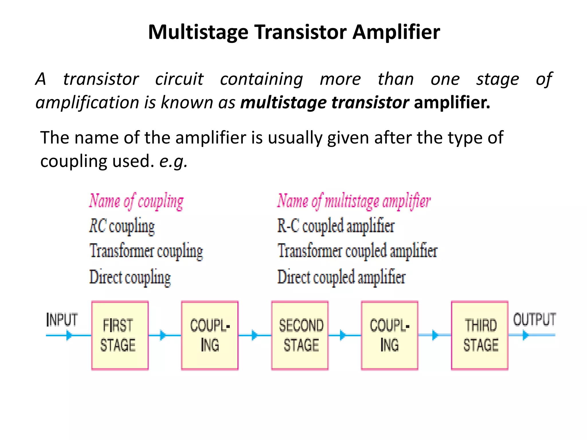
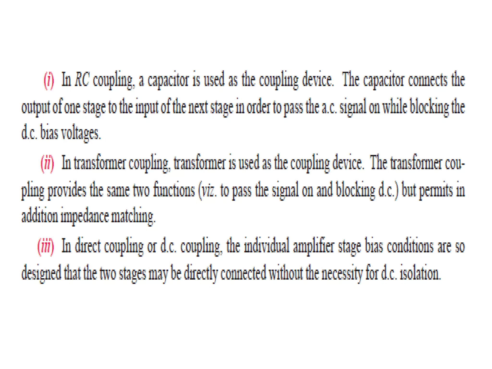
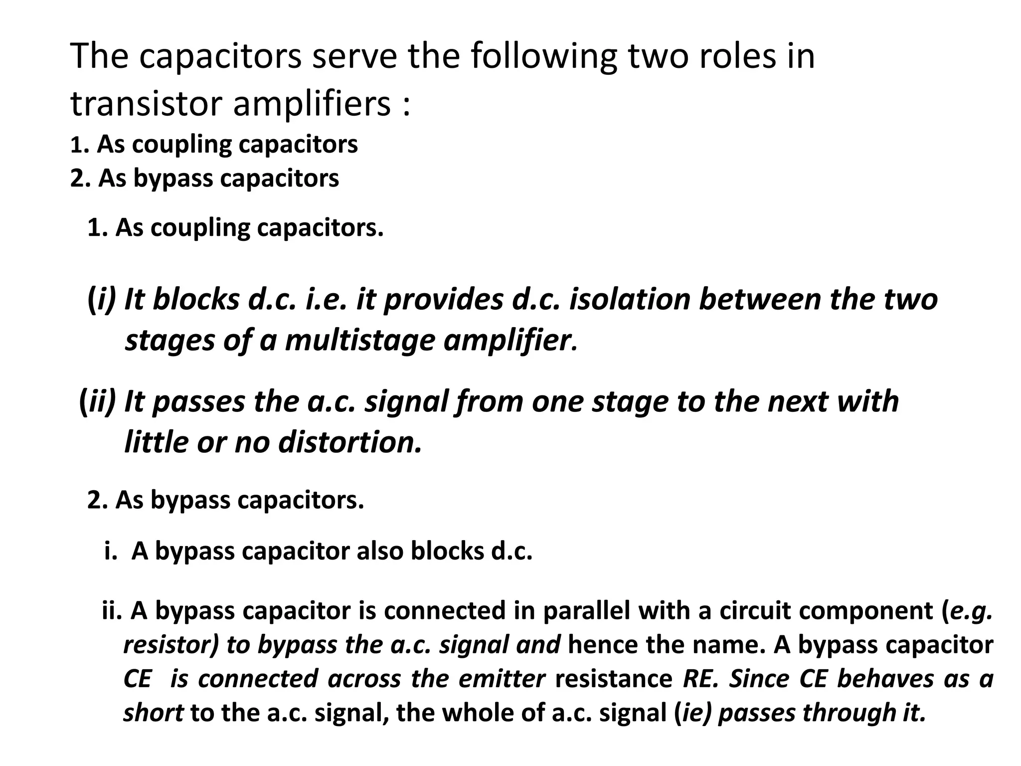
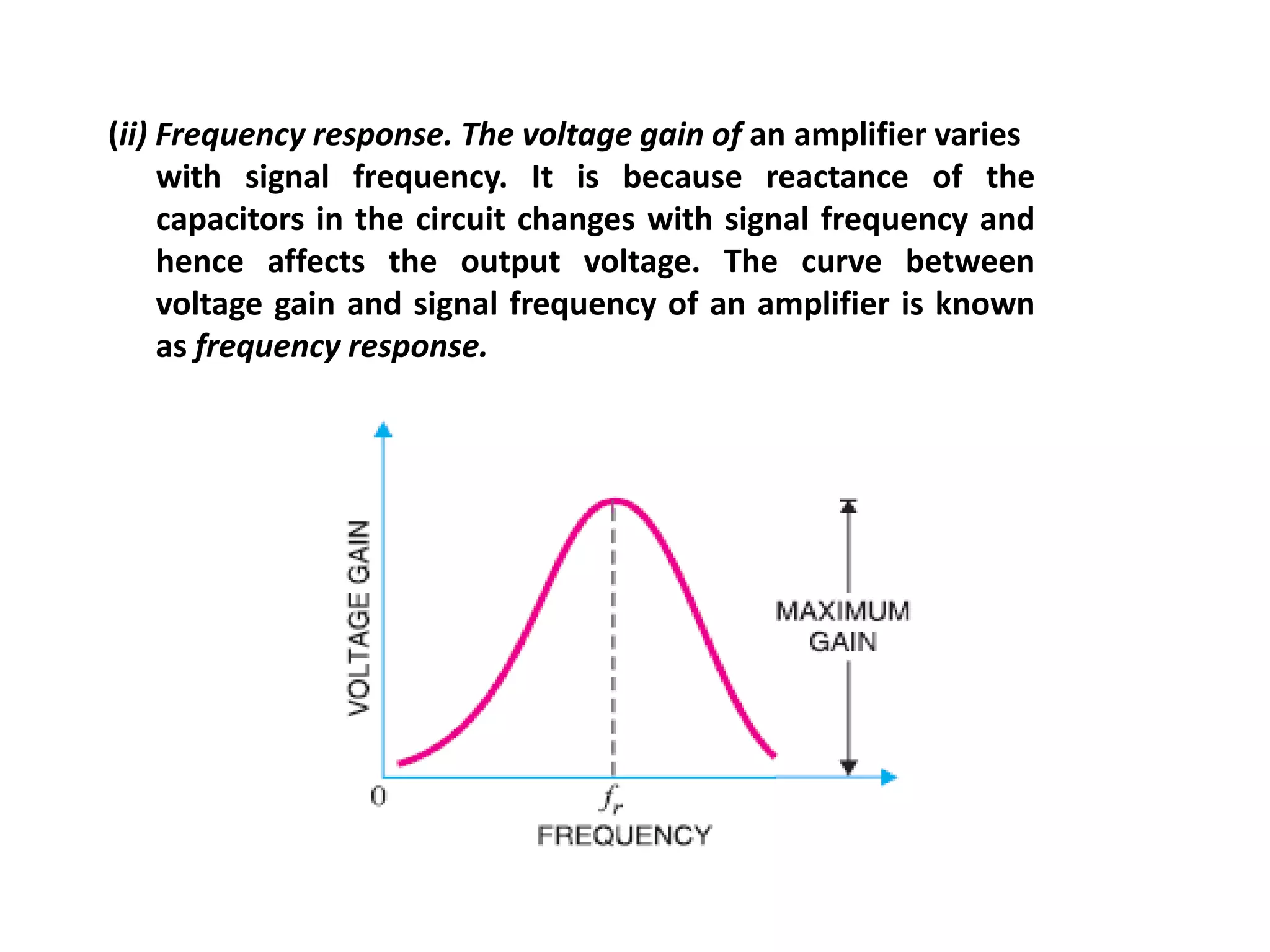
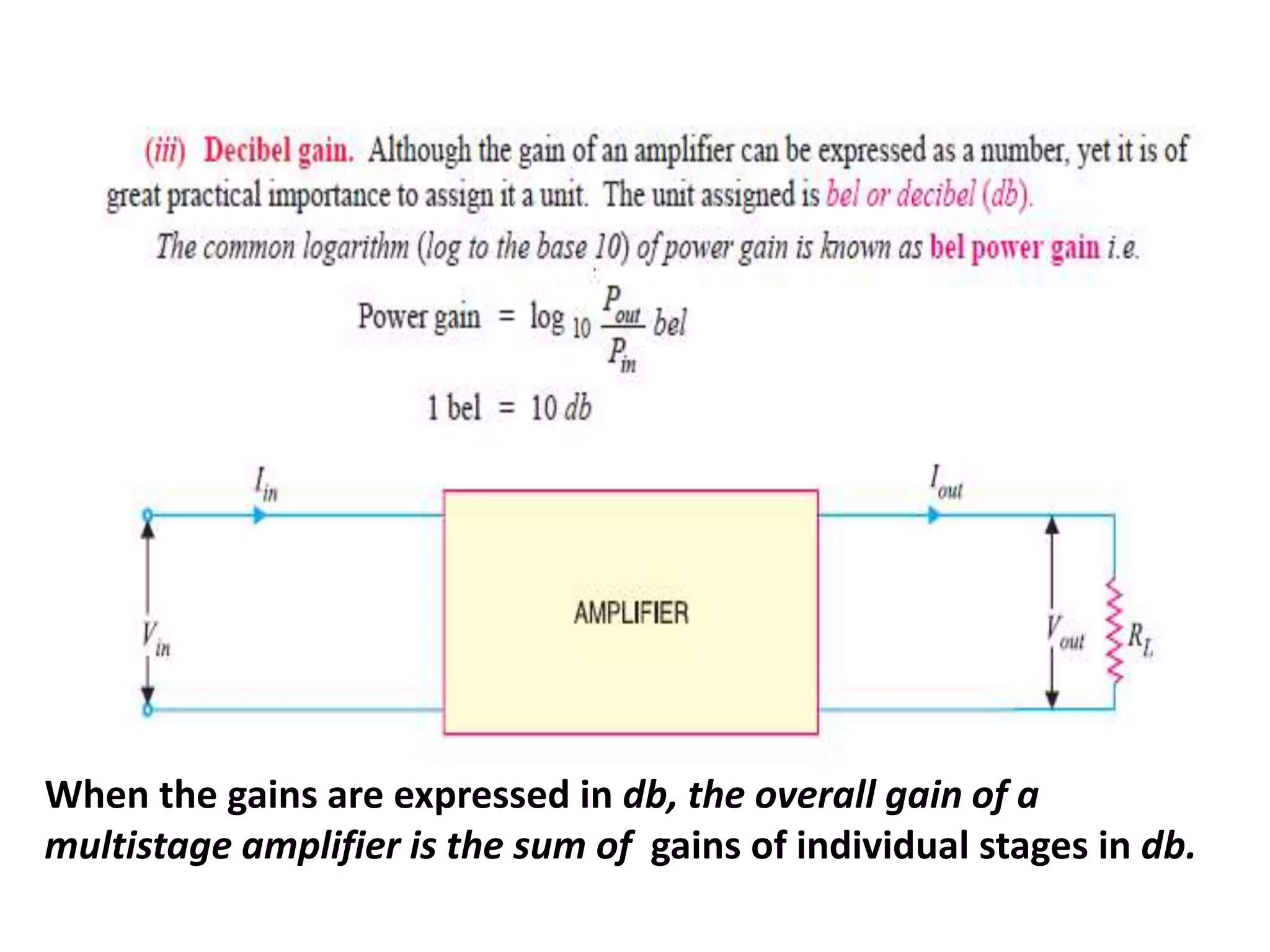
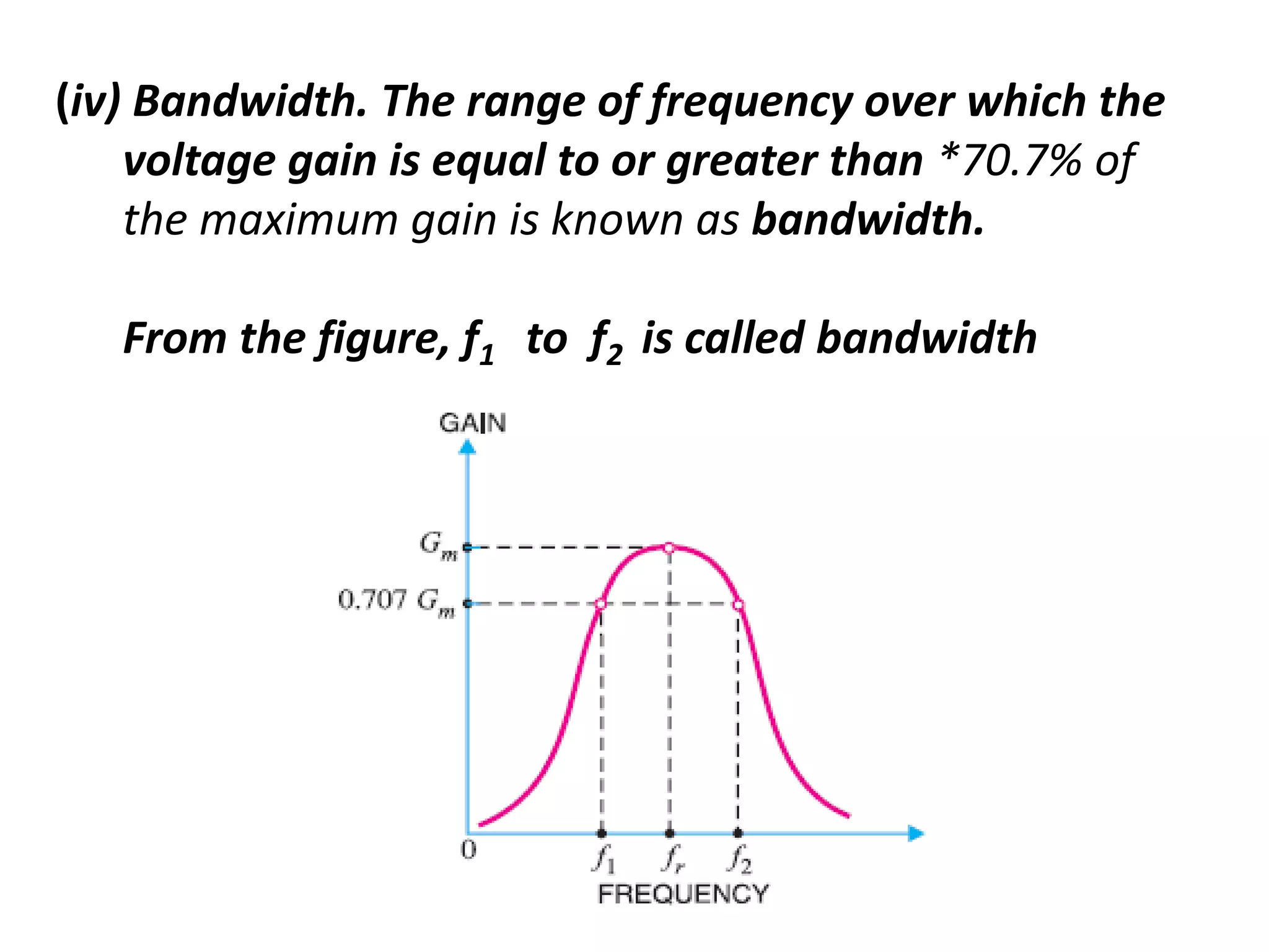
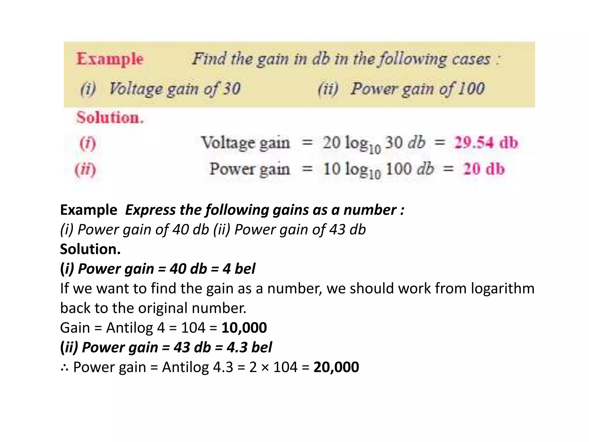
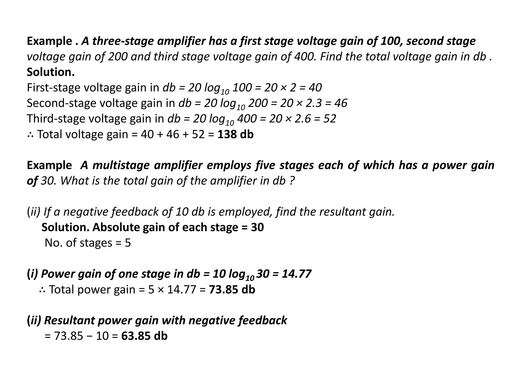
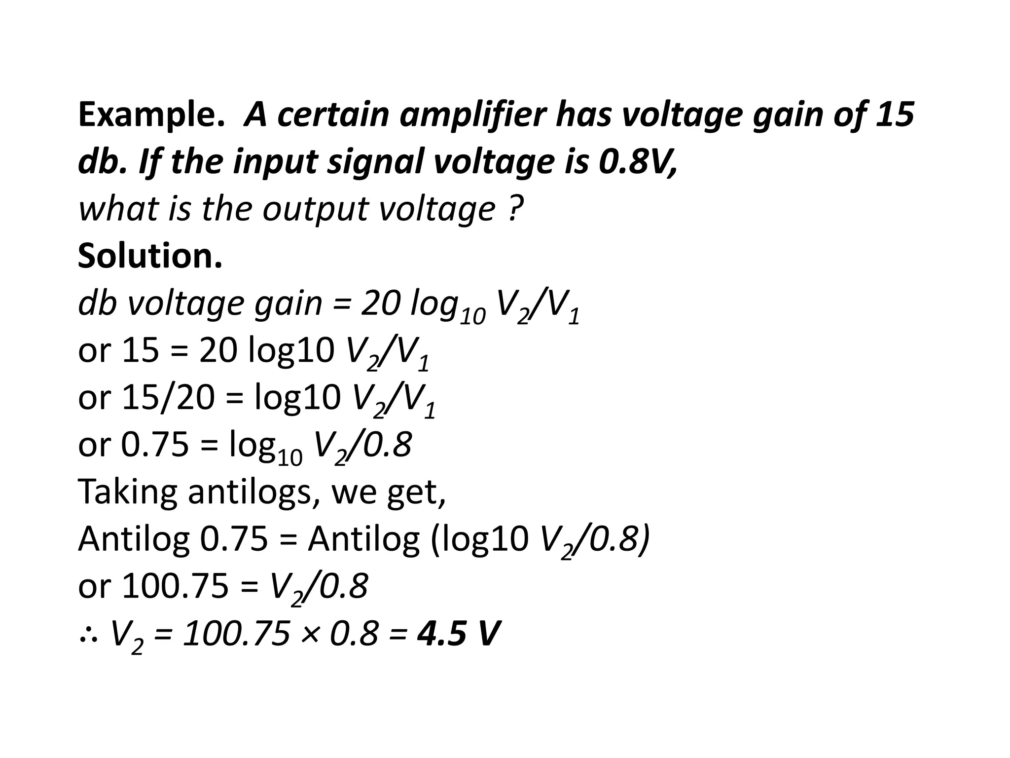
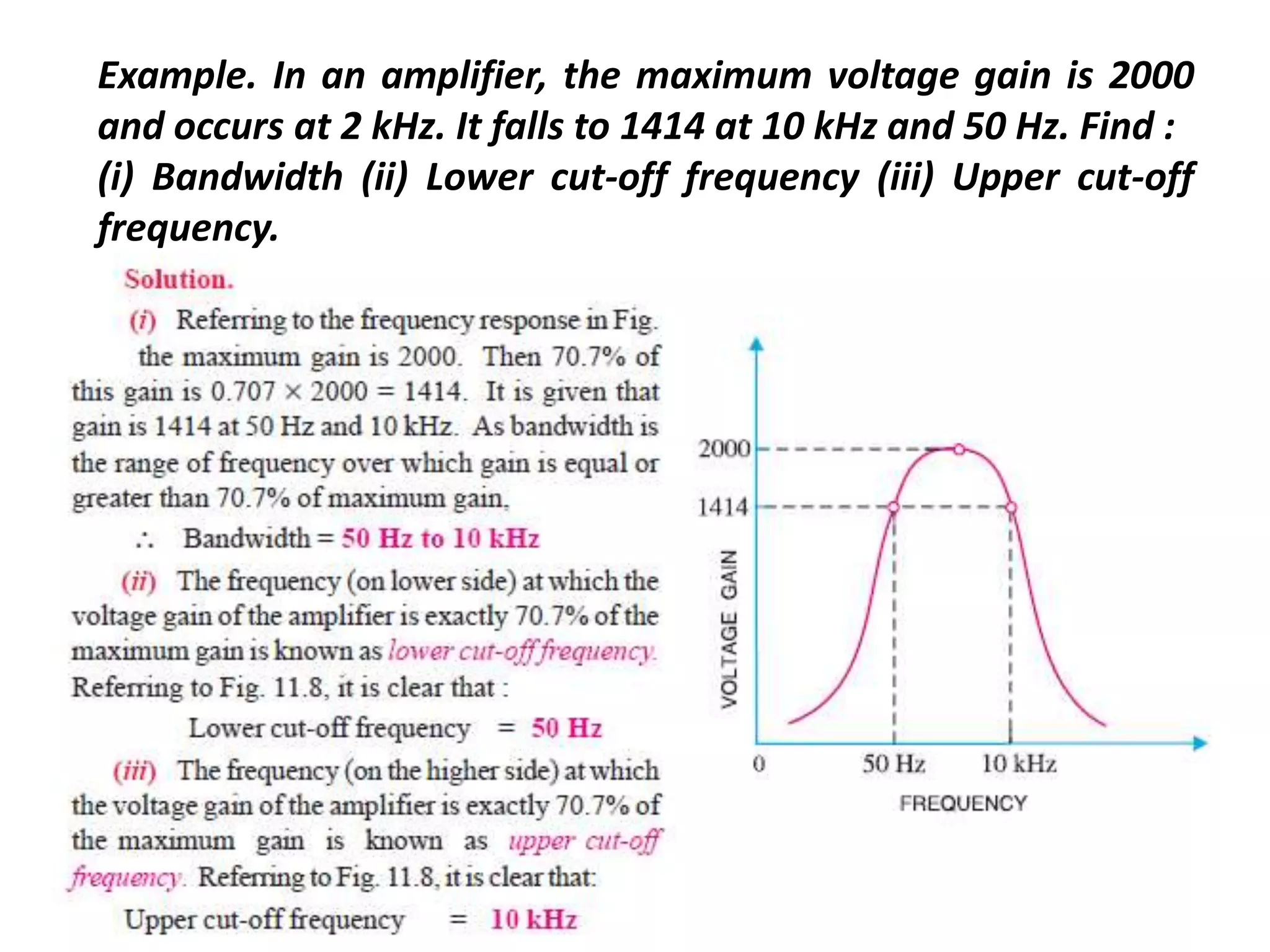
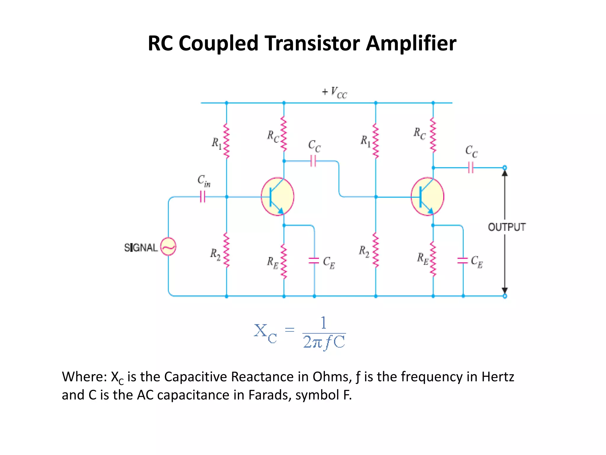
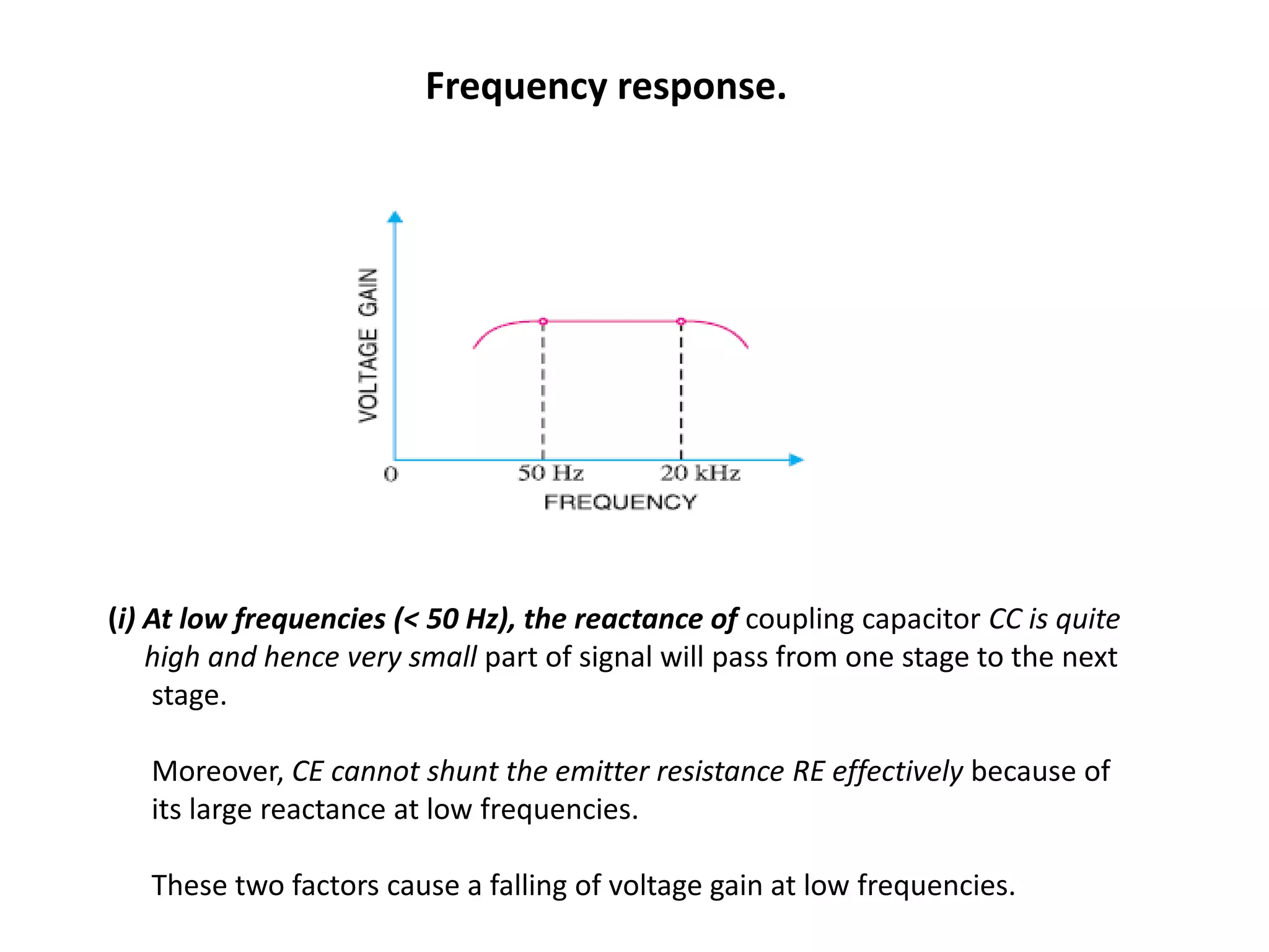
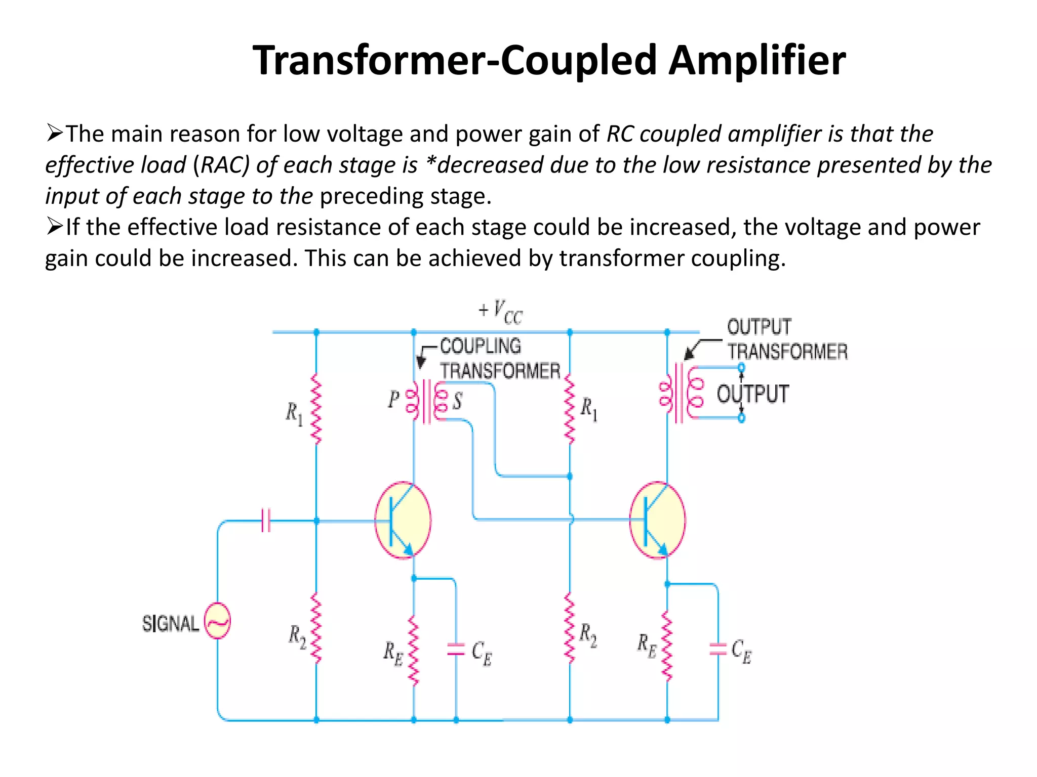
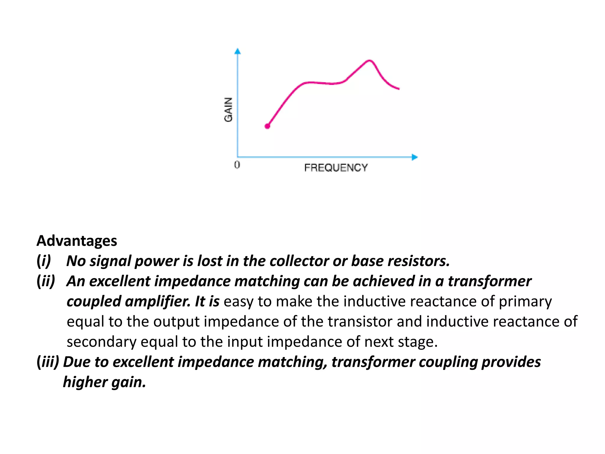
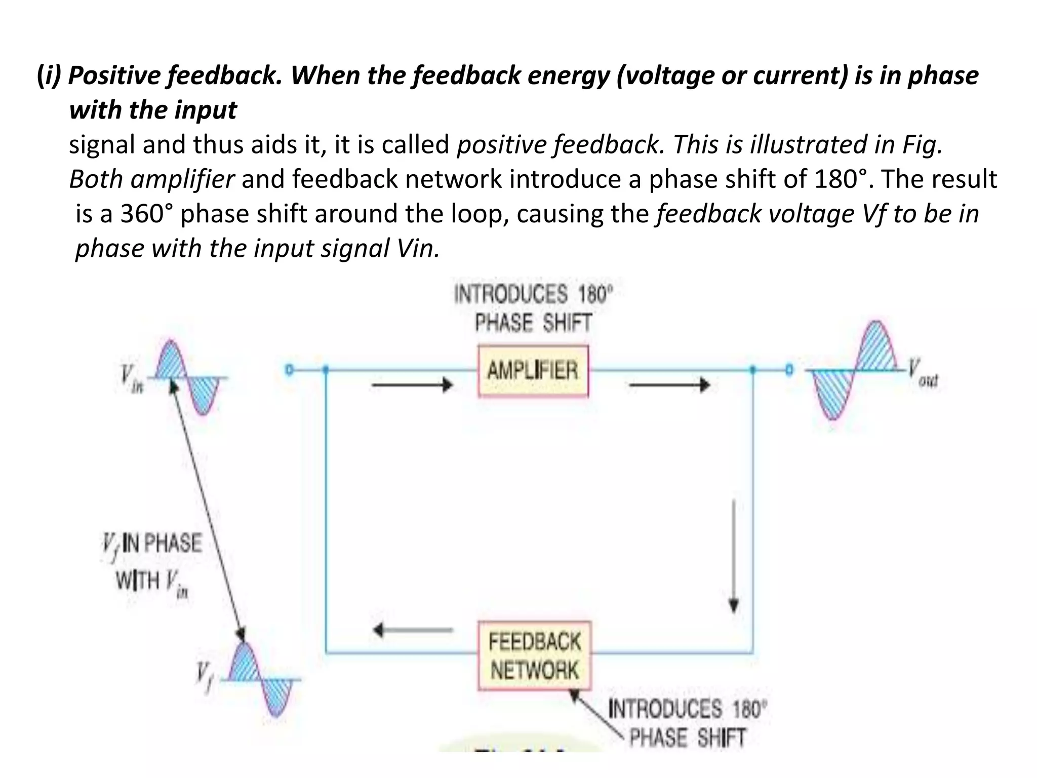
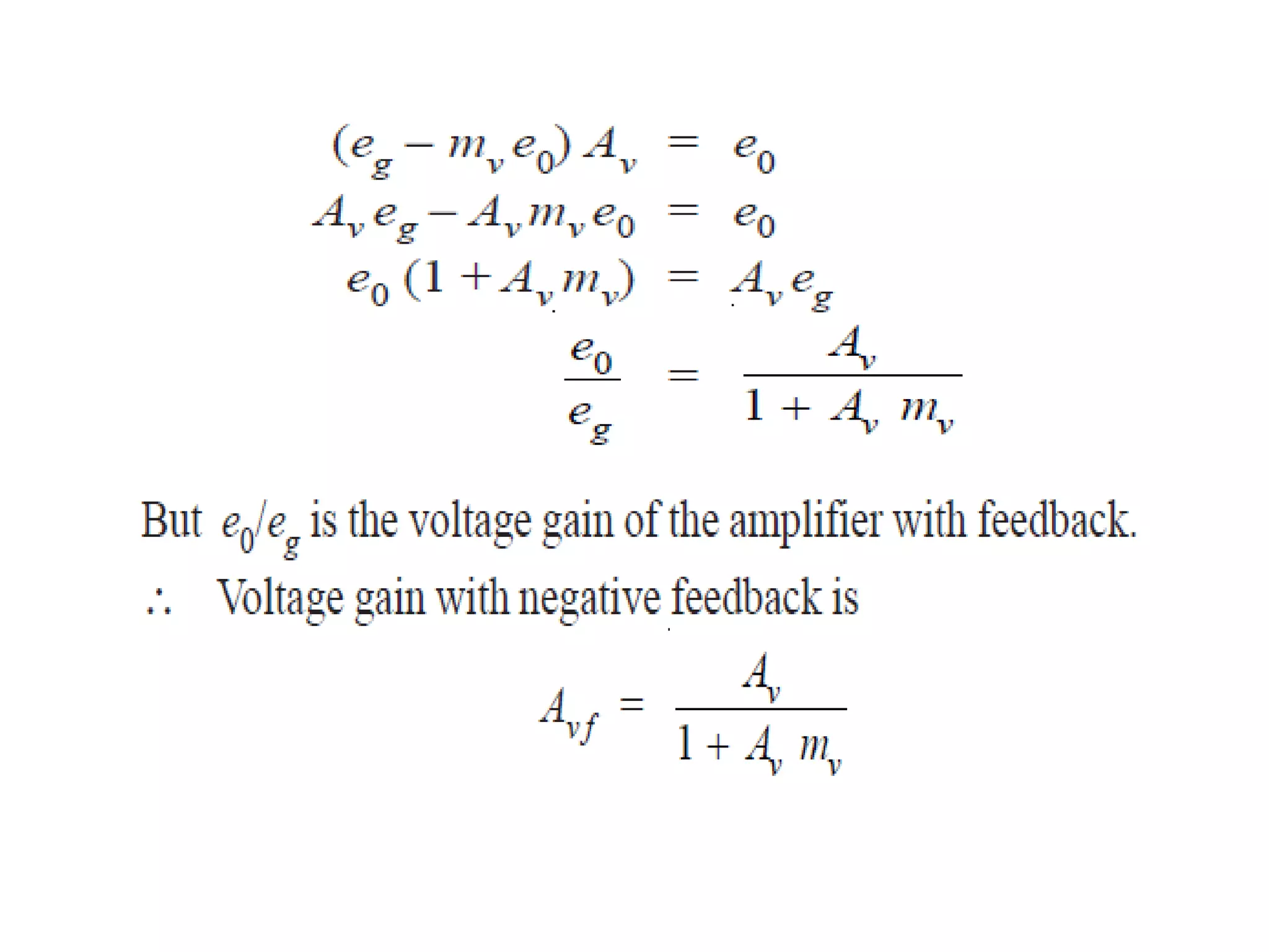
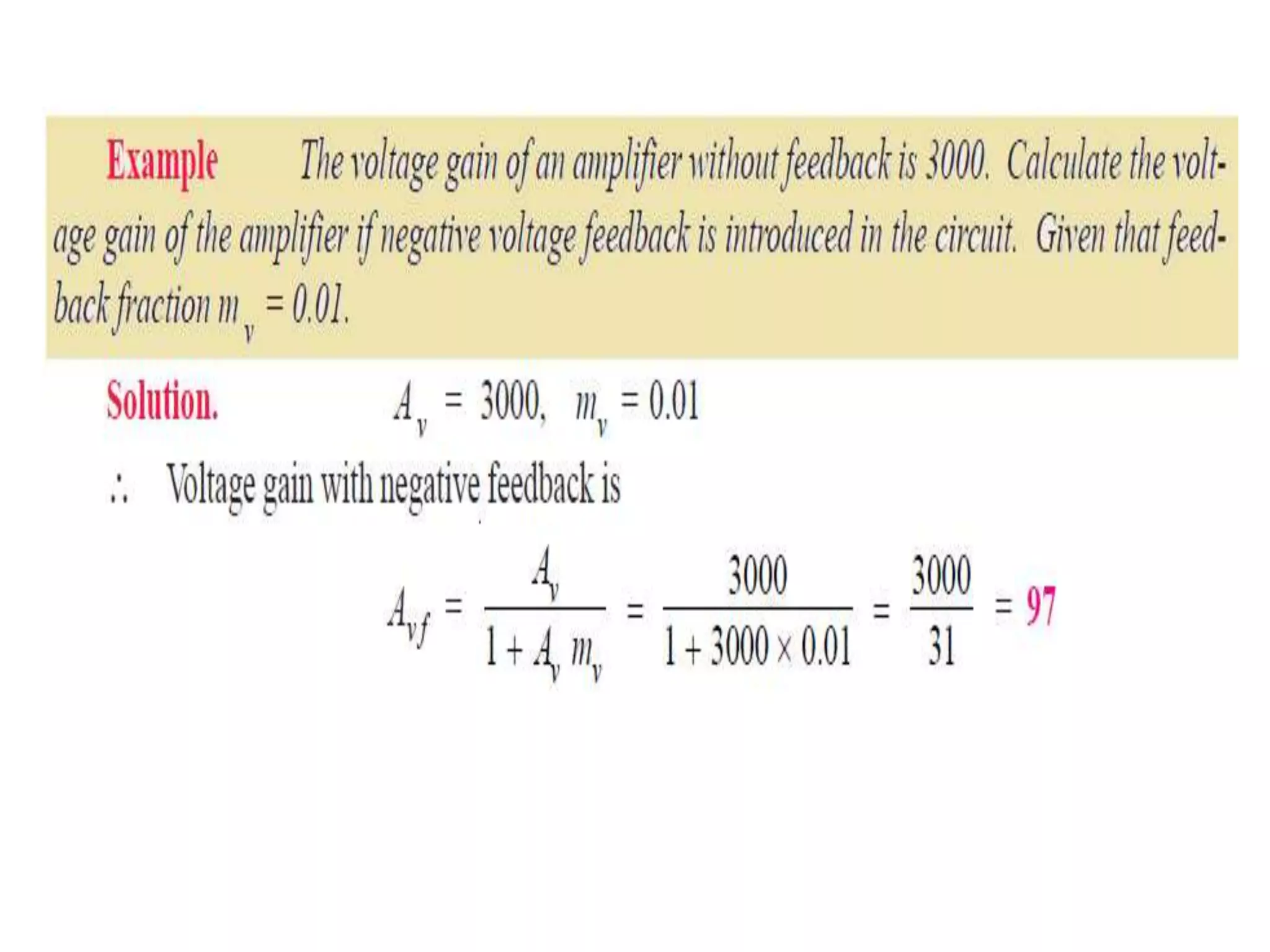
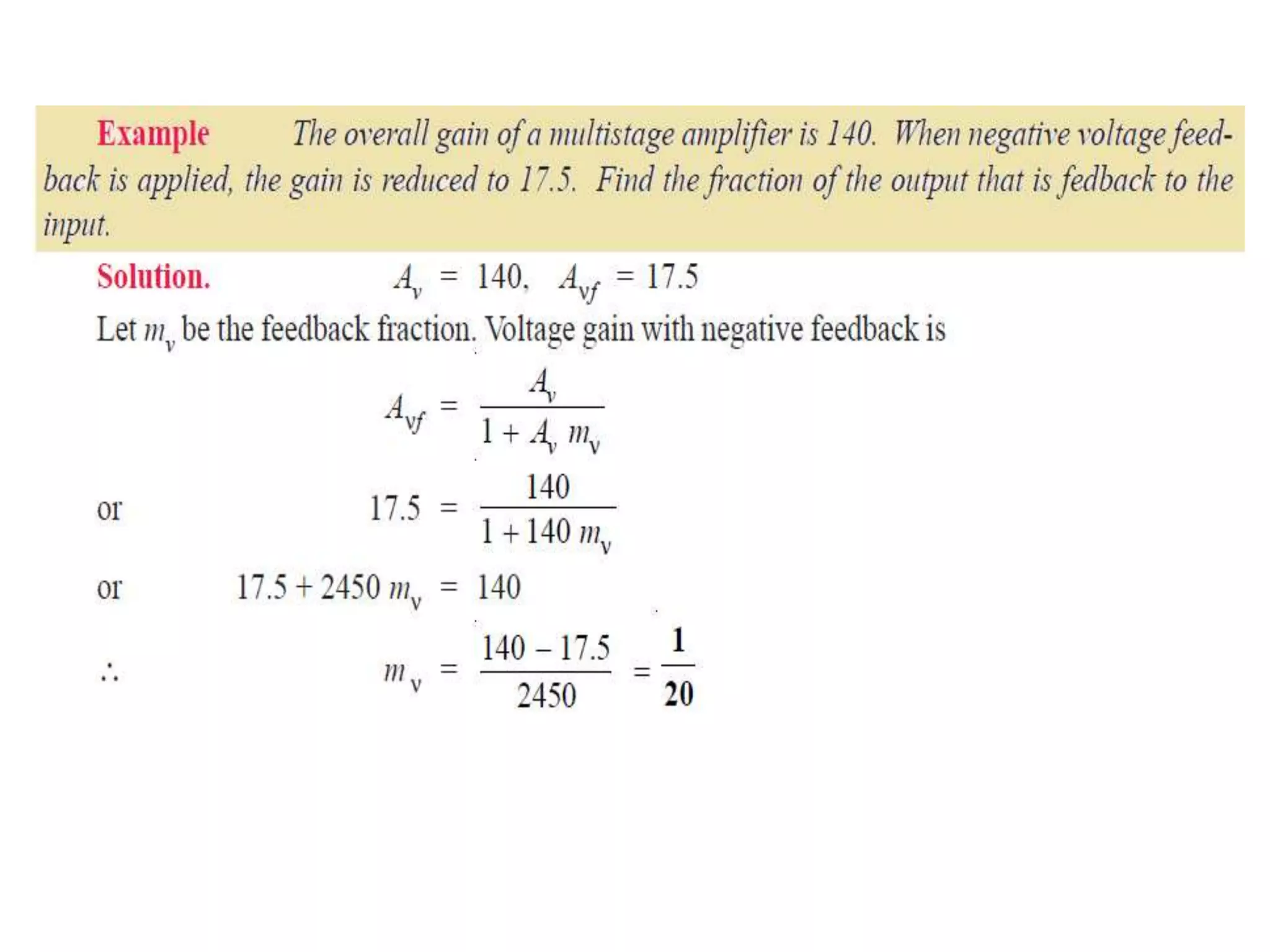
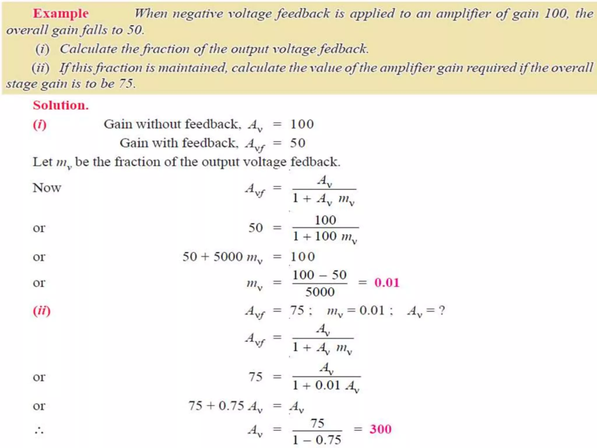
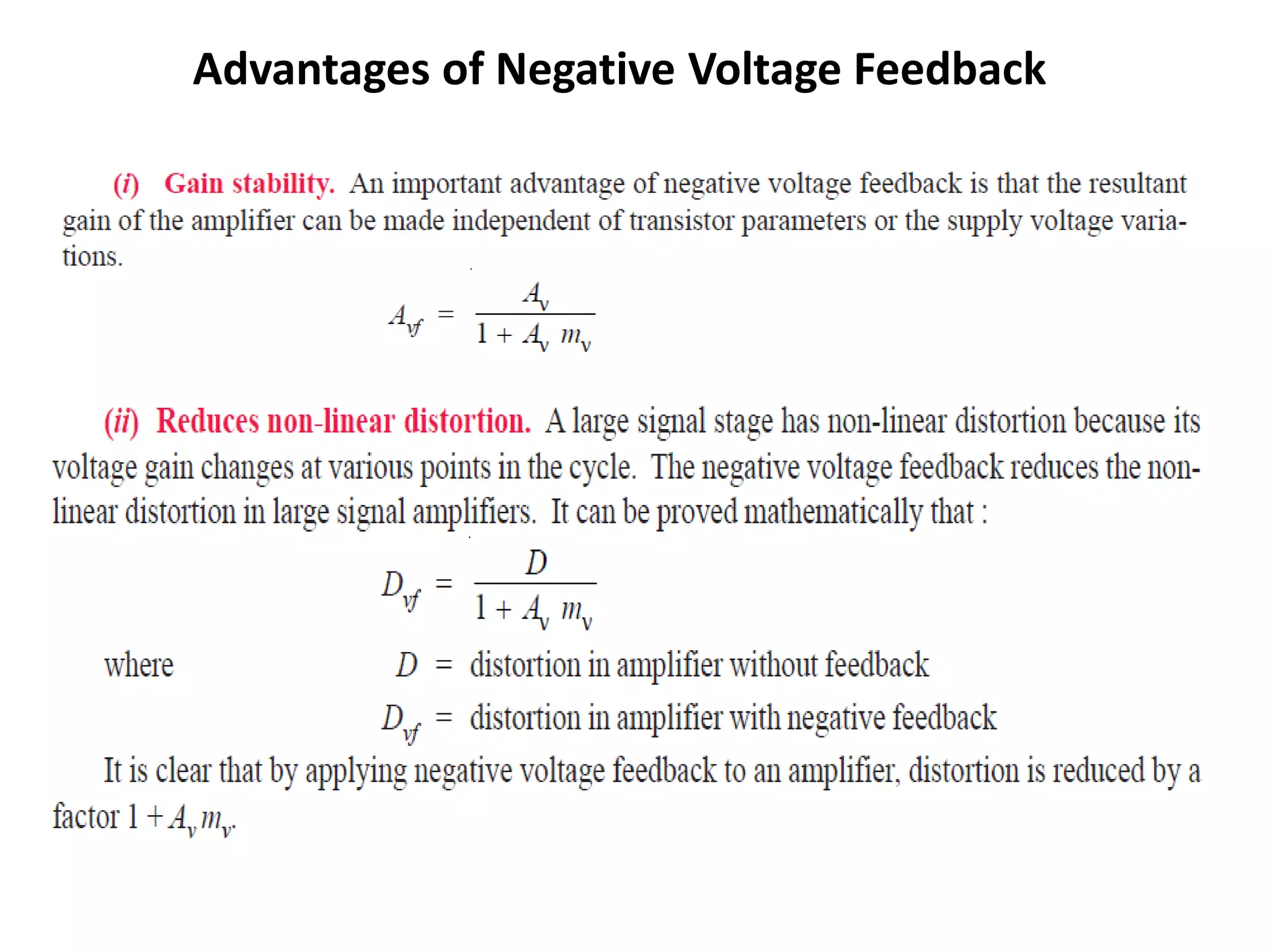
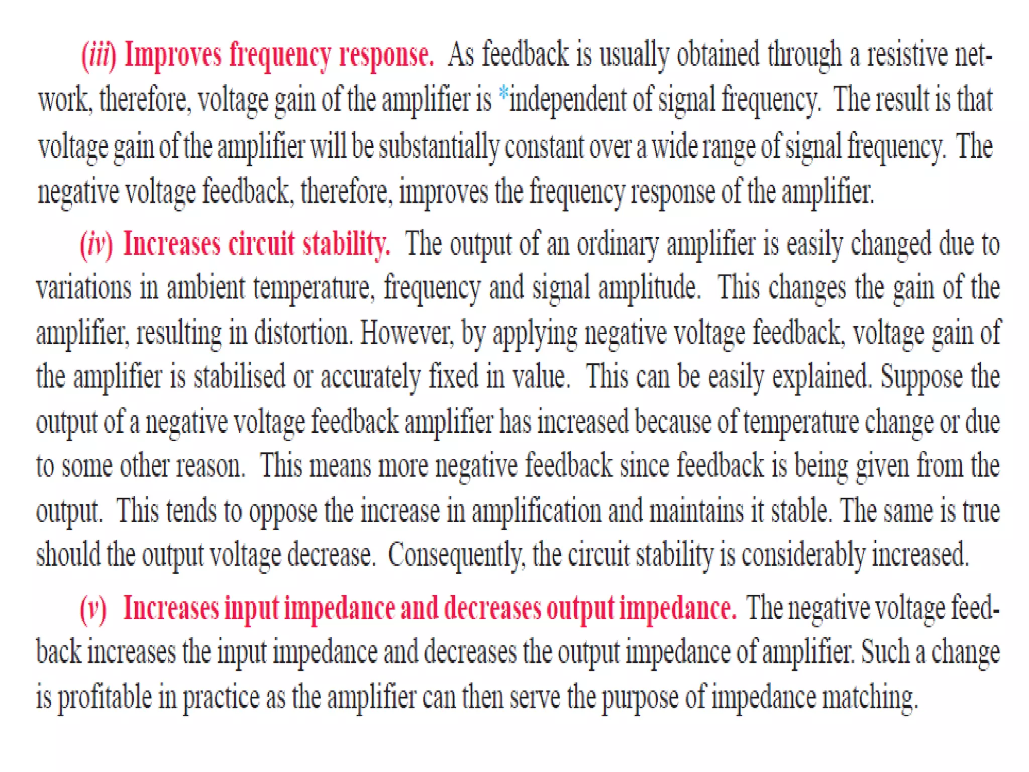
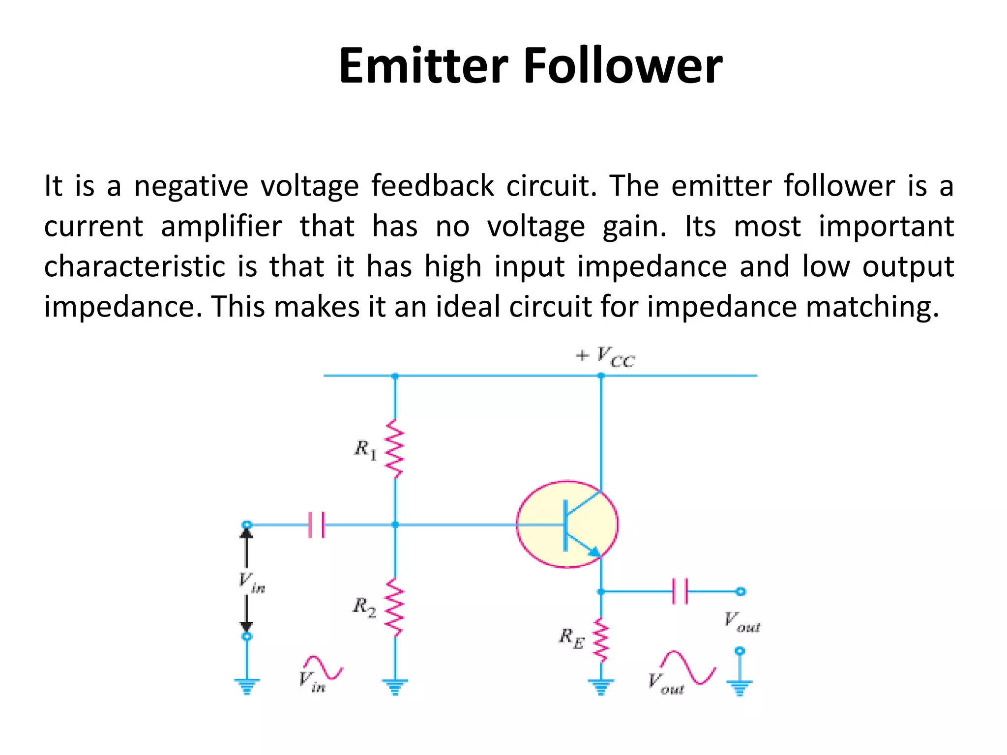
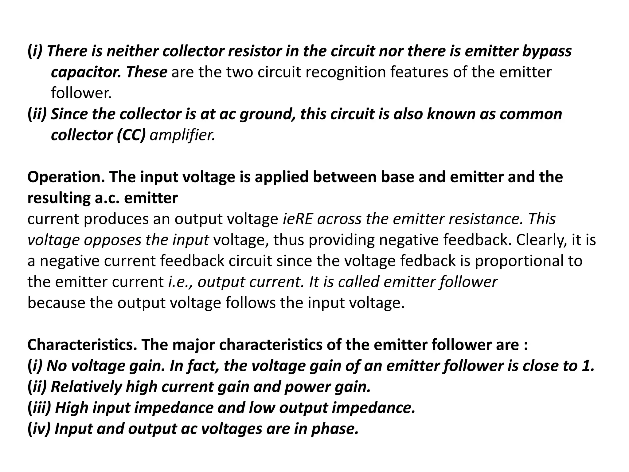
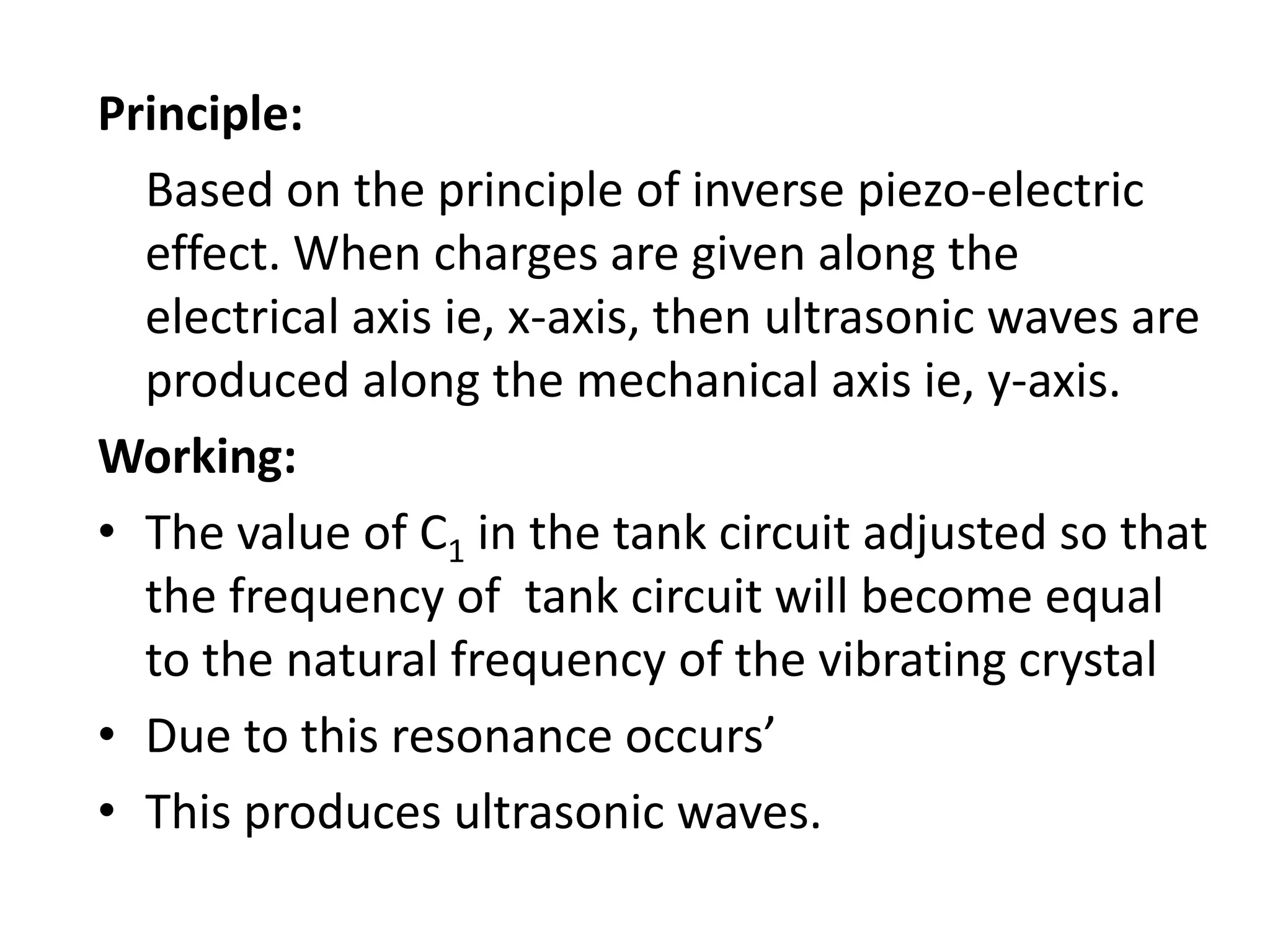
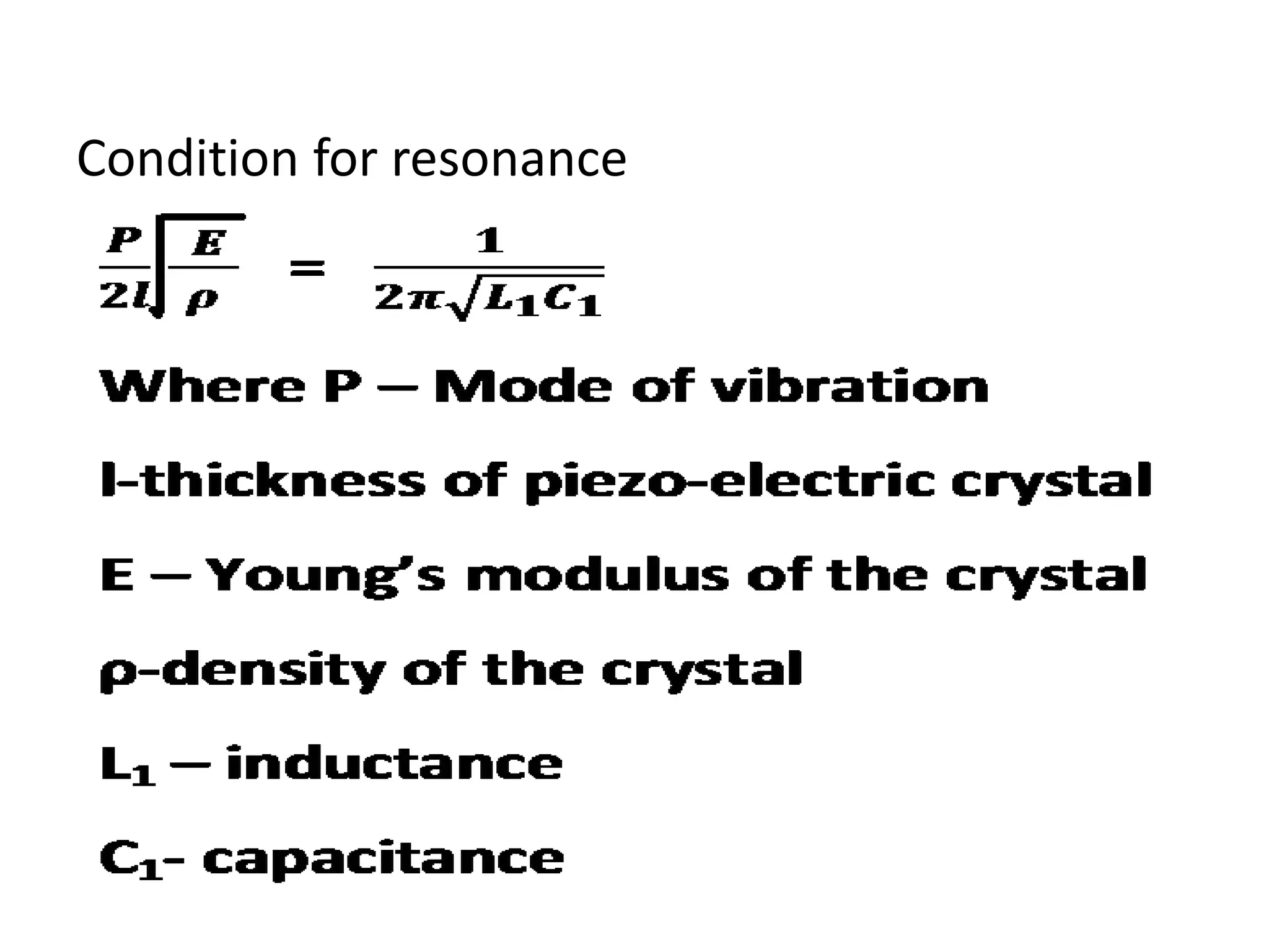
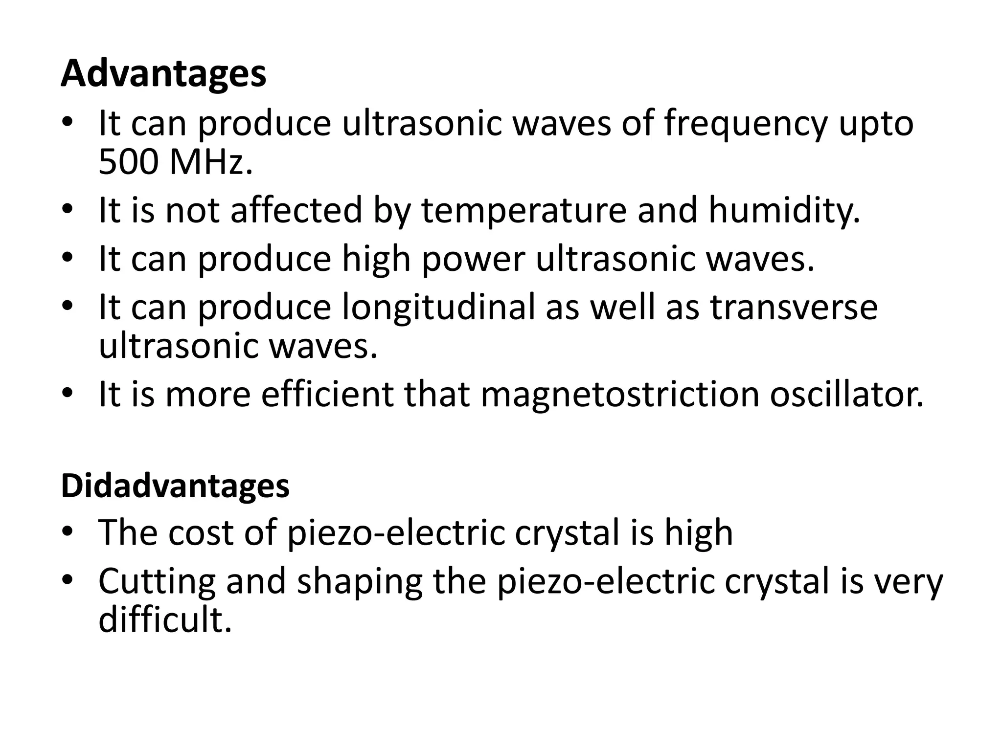
Dr. V. Mathivanan
Associate Professor of Physics
E.mail: mr.mathivanan@rediffmail.com
Multistage Transistor Amplifier
A transistor circuit containing more than one stage of
amplification is known as multistage transistor amplifier.
The name of the amplifier is usually given after the type of
coupling used. e.g.
The capacitors serve the following two roles in
transistor amplifiers :
1. As coupling capacitors
2. As bypass capacitors
1. As coupling capacitors.
(i) It blocks d.c. i.e. it provides d.c. isolation between the two
stages of a multistage amplifier.
(ii) It passes the a.c. signal from one stage to the next with
little or no distortion.
2. As bypass capacitors.
i. A bypass capacitor also blocks d.c.
ii. A bypass capacitor is connected in parallel with a circuit component (e.g.
resistor) to bypass the a.c. signal and hence the name. A bypass capacitor
CE is connected across the emitter resistance RE. Since CE behaves as a
short to the a.c. signal, the whole of a.c. signal (ie) passes through it.
Important Terms
(i) Gain. The ratio of the output *electrical quantity to
the input one of the amplifier is called its gain.
For instance, if G1, G2 and G3 are the individual
voltage gains of a three-stage amplifier, then total
voltage gain G is given by :
*G = G1 × G2 × G3
It is worthwhile to mention here that in practice,
total gain G is less than G1 × G2 × G3 due to the
loading effect of next stages.
(ii) Frequency response. The voltage gain of an amplifier varies
with signal frequency. It is because reactance of the
capacitors in the circuit changes with signal frequency and
hence affects the output voltage. The curve between
voltage gain and signal frequency of an amplifier is known
as frequency response.
When the gains are expressed in db, the overall gain of a
multistage amplifier is the sum of gains of individual stages in db.
(iv) Bandwidth. The range of frequency over which the
voltage gain is equal to or greater than *70.7% of
the maximum gain is known as bandwidth.
From the figure, f1 to f2 is called bandwidth
Example Express the following gains as a number :
(i) Power gain of 40 db (ii) Power gain of 43 db
Solution.
(i) Power gain = 40 db = 4 bel
If we want to find the gain as a number, we should work from logarithm
back to the original number.
Gain = Antilog 4 = 104 = 10,000
(ii) Power gain = 43 db = 4.3 bel
∴ Power gain = Antilog 4.3 = 2 × 104 = 20,000
Example . A three-stage amplifier has a first stage voltage gain of 100, second stage
voltage gain of 200 and third stage voltage gain of 400. Find the total voltage gain in db .
Solution.
First-stage voltage gain in db = 20 log10 100 = 20 × 2 = 40
Second-stage voltage gain in db = 20 log10 200 = 20 × 2.3 = 46
Third-stage voltage gain in db = 20 log10 400 = 20 × 2.6 = 52
∴ Total voltage gain = 40 + 46 + 52 = 138 db
Example A multistage amplifier employs five stages each of which has a power gain
of 30. What is the total gain of the amplifier in db ?
(ii) If a negative feedback of 10 db is employed, find the resultant gain.
Solution. Absolute gain of each stage = 30
No. of stages = 5
(i) Power gain of one stage in db = 10 log10 30 = 14.77
∴ Total power gain = 5 × 14.77 = 73.85 db
(ii) Resultant power gain with negative feedback
= 73.85 − 10 = 63.85 db
Example. A certain amplifier has voltage gain of 15
db. If the input signal voltage is 0.8V,
what is the output voltage ?
Solution.
db voltage gain = 20 log10 V2/V1
or 15 = 20 log10 V2/V1
or 15/20 = log10 V2/V1
or 0.75 = log10 V2/0.8
Taking antilogs, we get,
Antilog 0.75 = Antilog (log10 V2/0.8)
or 100.75 = V2/0.8
∴ V2 = 100.75 × 0.8 = 4.5 V
Example. In an amplifier, the maximum voltage gain is 2000
and occurs at 2 kHz. It falls to 1414 at 10 kHz and 50 Hz. Find :
(i) Bandwidth (ii) Lower cut-off frequency (iii) Upper cut-off
frequency.
RC Coupled Transistor Amplifier
Where: XC is the Capacitive Reactance in Ohms, ƒ is the frequency in Hertz
and C is the AC capacitance in Farads, symbol F.
This is the most popular type of coupling because it is cheap and provides
excellent audio fidelity over a wide range of frequency.
It is usually employed for voltage amplification. Fig. shows two stages of an RC
coupled amplifier. A coupling capacitor CC is used to connect the output of
first stage to the base (i.e. input) of the second stage and so on.
As the coupling from one stage to next is achieved by a coupling capacitor
followed by a connection to a shunt resistor, therefore, such amplifiers are
called resistance – capacitance coupled amplifiers.
The resistances R1, R2 and RE form the biasing and stabilization network.
The emitter bypass capacitor offers low reactance path to the signal. Without
it, the voltage gain of each stage would be lost.
The coupling capacitor CC transmits a.c. signal but blocks d.c. This prevents
d.c. interference between various stages and the shifting of operating point.
Operation. When a.c. signal is applied to the base of the first
transistor, it appears in the amplified form across its collector
load RC.
The amplified signal developed across RC is given to base of
next stage through coupling capacitor CC.
The second stage does further amplification of the signal. In
this way, the cascaded (one after another) stages amplify the
signal and the overall gain is considerably increased.
It may be mentioned here that total gain is less than the
product of the gains of individual stages.
It is because when a second stage is made to follow the first
stage, the effective load resistance of first stage is reduced
due to the shunting effect of the input resistance of second
stage.
Frequency response.
(i) At low frequencies (< 50 Hz), the reactance of coupling capacitor CC is quite
high and hence very small part of signal will pass from one stage to the next
stage.
Moreover, CE cannot shunt the emitter resistance RE effectively because of
its large reactance at low frequencies.
These two factors cause a falling of voltage gain at low frequencies.
(ii) At high frequencies (> 20 kHz), the reactance of CC is very small
and it behaves as a short circuit.
 This increases the loading effect of next stage and serves to
reduce the voltage gain.
 Moreover, at high frequency, capacitive reactance of base-
emitter junction is low which increases the base current. This
reduces the current amplification factor β.
Due to these two reasons, the voltage gain drops off at high
frequency.
(iii) At mid-frequencies (50 Hz to 20 kHz), the voltage gain of the
amplifier is constant.
The effect of coupling capacitor in this frequency range is such so as
to maintain a uniform voltage gain.
Thus, as the frequency increases in this range, reactance of CC
decreases which tends to increase the gain.
However, at the same time, lower reactance means higher loading of
first stage and hence lower gain.
These two factors almost cancel each other, resulting in a uniform gain
at mid-frequency.
Transformer-Coupled Amplifier
The main reason for low voltage and power gain of RC coupled amplifier is that the
effective load (RAC) of each stage is *decreased due to the low resistance presented by the
input of each stage to the preceding stage.
If the effective load resistance of each stage could be increased, the voltage and power
gain could be increased. This can be achieved by transformer coupling.
Operation. When an a.c. signal is applied to the base of first transistor, it appears in
the amplified form across primary P of the coupling transformer.
 The voltage developed across primary is transferred to the input of the next stage
by the transformer secondary as shown in Fig.
 The second stage renders amplification in an exactly similar manner.
Frequency response. The frequency response of a transformer coupled
amplifier is shown in Fig. It is clear that frequency response is rather poor i.e.
gain is constant only over a small range of frequency.
The output voltage is equal to the collector current multiplied by reactance of
primary.
At low frequencies, the reactance of primary begins to fall, resulting in
decreased gain. At high frequencies, the capacitance between turns of windings
acts as a bypass condenser to reduce the output voltage and hence gain.
It follows, therefore, that there will be disproportionate amplification of
frequencies in a complete signal such as music, speech etc. Hence, transformer-
coupled amplifier introduces frequency distortion.
Advantages
(i) No signal power is lost in the collector or base resistors.
(ii) An excellent impedance matching can be achieved in a transformer
coupled amplifier. It is easy to make the inductive reactance of primary
equal to the output impedance of the transistor and inductive reactance of
secondary equal to the input impedance of next stage.
(iii) Due to excellent impedance matching, transformer coupling provides
higher gain.
Disadvantages
(i) It has a poor frequency response i.e.the gain varies
considerably with frequency.
(ii) The coupling transformers are bulky and fairly expensive at
audio frequencies.
(iii) Frequency distortion is higher i.e. low frequency signals are
less amplified as compared to the high frequency signals.
(iv) Transformer coupling tends to introduce *hum in the
output.
Applications. Transformer coupling is mostly
employed for impedance matching. In general, the
last stage of a multistage amplifier is the power stage.
Here, a concentrated effort is made to transfer
maximum power to the output device e.g. a
loudspeaker.
Feedback
The process of injecting a fraction of output
energy of some device back to the input is
known as feedback.
It has been found very useful in reducing
noise in amplifiers and making amplifier
operation stable.
(i) Positive feedback. When the feedback energy (voltage or current) is in phase
with the input
signal and thus aids it, it is called positive feedback. This is illustrated in Fig.
Both amplifier and feedback network introduce a phase shift of 180°. The result
is a 360° phase shift around the loop, causing the feedback voltage Vf to be in
phase with the input signal Vin.
The positive feedback increases the gain of
the amplifier.
However, it has the disadvantages of
increased distortion and instability.
Therefore, positive feedback is seldom
employed in amplifiers.
One important use of positive feedback is
in oscillators.
(ii) Negative feedback. When the feedback energy
(voltage or current) is out of phase with the
input signal and thus opposes it, it is called negative feedback. This is illustrated in
Fig. As you can see, the amplifier introduces a phase shift of 180° into the circuit
while the feedback network is so designed that it introduces no phase shift (i.e., 0°
phase shift). The result is that the feedback voltage Vf is 180° out of
phase with the input signal Vin.
Negative feedback reduces the gain of the
amplifier.
However, the advantages of negative
feedback are: reduction in distortion,
stability in gain, increased bandwidth and
improved input and output impedances.
It is due to these advantages that negative
feedback is frequently employed in
amplifiers.
Gain of Negative Voltage Feedback Amplifier
Advantages of Negative Voltage Feedback
Emitter Follower
It is a negative voltage feedback circuit. The emitter follower is a
current amplifier that has no voltage gain. Its most important
characteristic is that it has high input impedance and low output
impedance. This makes it an ideal circuit for impedance matching.
(i) There is neither collector resistor in the circuit nor there is emitter bypass
capacitor. These are the two circuit recognition features of the emitter
follower.
(ii) Since the collector is at ac ground, this circuit is also known as common
collector (CC) amplifier.
Operation. The input voltage is applied between base and emitter and the
resulting a.c. emitter
current produces an output voltage ieRE across the emitter resistance. This
voltage opposes the input voltage, thus providing negative feedback. Clearly, it is
a negative current feedback circuit since the voltage fedback is proportional to
the emitter current i.e., output current. It is called emitter follower
because the output voltage follows the input voltage.
Characteristics. The major characteristics of the emitter follower are :
(i) No voltage gain. In fact, the voltage gain of an emitter follower is close to 1.
(ii) Relatively high current gain and power gain.
(iii) High input impedance and low output impedance.
(iv) Input and output ac voltages are in phase.
Applications of Emitter Follower
(i) To provide current amplification with no voltage gain.
(ii) Impedance matching.
(i) Current amplification without voltage gain. We know that an emitter
follower is a current amplifier that has no voltage gain (Aν j 1). There are
many instances (especially in digital electronics) where an increase in
current is required but no increase in voltage is needed. In such a situation,
an emitter follower can be used. For example, consider the two stage
amplifier circuit as shown in Fig. Suppose this 2-stage amplifier has
the desired voltage gain but current gain of this multistage amplifier is
insufficient. In that case, we can use an emitter follower to increase the
current gain without increasing the voltage gain.
(ii) Impedance matching. We know that an emitter follower has high input
impedance and low output impedance. This makes the emitter follower an
ideal circuit for impedance matching. Fig. shows the impedance matching by an
emitter follower. Here the output impedance of the source is 120 kΩ while that
of load is 20 Ω. The emitter follower has an input impedance of 120 kΩ and
output impedance of 22 Ω. It is connected between high-impedance source
and low impedance load. The net result of this arrangement is that maximum
power is transferred from the original source to the original load. When an
emitter follower is used for this purpose, it is called a buffer
amplifier.
Hartley Oscillator
The tank circuit is made up of L1, L2 and C. The frequency of oscillations is
determined by the values of L1, L2 and C and is given by :
Circuit operation. When the circuit is turned on, the capacitor is charged. When
this capacitor is fully charged, it discharges through coils L1 and L2 setting up
oscillations of frequency determined by *exp. (i). The output voltage of the
amplifier appears across L1 and feedback voltage across L2. The voltage across L2
is 180° out of phase with the voltage developed across L1 (Vout) as shown in Fig. .
It is easy to see that voltage fedback (i.e., voltage across L2) to the transistor
provides positive feedback. A phase shift of 180° is produced by the transistor and
a further phase shift of 180° is produced by L1 − L2 voltage divider. In this way,
feedback is properly phased to produce continuous undamped oscillations.
Circuit operation.
 When the circuit is turned on, the capacitor is charged.
 When this capacitor is fully charged, it discharges through coils L1 and L2
setting up oscillations of frequency.
 The output voltage of the amplifier appears across L1 and feedbackvoltage
across L2. The voltage across L2 is 180° out of phase with the voltage
developed across L1 (Vout) as shown in Fig. I
It is easy to see that voltage fedback (i.e., voltage across L2) to the
transistor provides positive feedback. A phase shift of 180° is produced by
the transistor and a further phase shift of 180° is produced by L1 − L2
voltage divider.
 In this way, feedback is properly phased to produce continuous undamped
oscillations.
Wien Bridge Oscillator
 The Wien-bridge oscillator is the standard oscillator circuit for all
frequencies in the range of 10 Hz to about 1 MHz.
It is the most frequently used type of audio oscillator as the output is
free from circuit fluctuations and ambient temperature. Fig. shows the
circuit of Wien bridge oscillator.
It is essentially a two-stage amplifier with R-C bridge circuit. The bridge
circuit has the arms R1C1, R3, R2C2 and tungsten lamp Lp.
 Resistances R3 and Lp are used to stabilise the amplitude of the
output.
The transistor T1 serves as an oscillator and amplifier while the other
transistor T2 serves as an inverter (i.e. to produce a phase shift of
180º).
The circuit uses positive and negative feedbacks. The positive feedback
is through R1C1, C2R2 to the transistor T1. The negative feedback is
through the voltage divider to the input of transistor T2. The frequency
of oscillations is determined by the series element R1C1 and parallel
element R2C2 of the bridge.
When the circuit is started, bridge circuit produces
oscillations of frequency.
The two transistors produce a total phase shift of 360º so
that proper positive feedback is ensured.
The negative feedback in the circuit ensures constant
output. This is achieved by the temperature sensitive
tungsten lamp Lp. Its resistance increases with current.
Should the amplitude of output tend to increase, more
current would provide more negative feedback. The result
is that the output would return to original value. A reverse
action would take place if the output tends to decrease.
Advantages
(i) It gives constant output.
(ii) The circuit works quite easily.
(iii) The overall gain is high because of two
transistors.
(iv) The frequency of oscillations can be easily
changed by using a potentiometer.
Disadvantages
(i) The circuit requires two transistors and a large
number of components.
(ii) It cannot generate very high frequencies.
• It consists of a transformer having primary and
secondary circuits.
• The primary circuits consist of a battery which
gives variable current, a npn transistor and a
tank circuit consisting of inductance and
capacitance connected in parallel.
• The secondary circuit consists of a coil L which
is given to a Piezo-electric crystal.
Principle:
Based on the principle of inverse piezo-electric
effect. When charges are given along the
electrical axis ie, x-axis, then ultrasonic waves are
produced along the mechanical axis ie, y-axis.
Working:
• The value of C1 in the tank circuit adjusted so that
the frequency of tank circuit will become equal
to the natural frequency of the vibrating crystal
• Due to this resonance occurs’
• This produces ultrasonic waves.
Condition for resonance
Advantages
• It can produce ultrasonic waves of frequency upto
500 MHz.
• It is not affected by temperature and humidity.
• It can produce high power ultrasonic waves.
• It can produce longitudinal as well as transverse
ultrasonic waves.
• It is more efficient that magnetostriction oscillator.
Didadvantages
• The cost of piezo-electric crystal is high
• Cutting and shaping the piezo-electric crystal is very
difficult.

Basic Electronics 4 by Dr. Mathivanan Velumani

  • 1.
    Dr. V. Mathivanan AssociateProfessor of Physics E.mail: mr.mathivanan@rediffmail.com
  • 2.
    Multistage Transistor Amplifier Atransistor circuit containing more than one stage of amplification is known as multistage transistor amplifier. The name of the amplifier is usually given after the type of coupling used. e.g.
  • 4.
    The capacitors servethe following two roles in transistor amplifiers : 1. As coupling capacitors 2. As bypass capacitors 1. As coupling capacitors. (i) It blocks d.c. i.e. it provides d.c. isolation between the two stages of a multistage amplifier. (ii) It passes the a.c. signal from one stage to the next with little or no distortion. 2. As bypass capacitors. i. A bypass capacitor also blocks d.c. ii. A bypass capacitor is connected in parallel with a circuit component (e.g. resistor) to bypass the a.c. signal and hence the name. A bypass capacitor CE is connected across the emitter resistance RE. Since CE behaves as a short to the a.c. signal, the whole of a.c. signal (ie) passes through it.
  • 5.
    Important Terms (i) Gain.The ratio of the output *electrical quantity to the input one of the amplifier is called its gain. For instance, if G1, G2 and G3 are the individual voltage gains of a three-stage amplifier, then total voltage gain G is given by : *G = G1 × G2 × G3 It is worthwhile to mention here that in practice, total gain G is less than G1 × G2 × G3 due to the loading effect of next stages.
  • 6.
    (ii) Frequency response.The voltage gain of an amplifier varies with signal frequency. It is because reactance of the capacitors in the circuit changes with signal frequency and hence affects the output voltage. The curve between voltage gain and signal frequency of an amplifier is known as frequency response.
  • 7.
    When the gainsare expressed in db, the overall gain of a multistage amplifier is the sum of gains of individual stages in db.
  • 8.
    (iv) Bandwidth. Therange of frequency over which the voltage gain is equal to or greater than *70.7% of the maximum gain is known as bandwidth. From the figure, f1 to f2 is called bandwidth
  • 9.
    Example Express thefollowing gains as a number : (i) Power gain of 40 db (ii) Power gain of 43 db Solution. (i) Power gain = 40 db = 4 bel If we want to find the gain as a number, we should work from logarithm back to the original number. Gain = Antilog 4 = 104 = 10,000 (ii) Power gain = 43 db = 4.3 bel ∴ Power gain = Antilog 4.3 = 2 × 104 = 20,000
  • 10.
    Example . Athree-stage amplifier has a first stage voltage gain of 100, second stage voltage gain of 200 and third stage voltage gain of 400. Find the total voltage gain in db . Solution. First-stage voltage gain in db = 20 log10 100 = 20 × 2 = 40 Second-stage voltage gain in db = 20 log10 200 = 20 × 2.3 = 46 Third-stage voltage gain in db = 20 log10 400 = 20 × 2.6 = 52 ∴ Total voltage gain = 40 + 46 + 52 = 138 db Example A multistage amplifier employs five stages each of which has a power gain of 30. What is the total gain of the amplifier in db ? (ii) If a negative feedback of 10 db is employed, find the resultant gain. Solution. Absolute gain of each stage = 30 No. of stages = 5 (i) Power gain of one stage in db = 10 log10 30 = 14.77 ∴ Total power gain = 5 × 14.77 = 73.85 db (ii) Resultant power gain with negative feedback = 73.85 − 10 = 63.85 db
  • 11.
    Example. A certainamplifier has voltage gain of 15 db. If the input signal voltage is 0.8V, what is the output voltage ? Solution. db voltage gain = 20 log10 V2/V1 or 15 = 20 log10 V2/V1 or 15/20 = log10 V2/V1 or 0.75 = log10 V2/0.8 Taking antilogs, we get, Antilog 0.75 = Antilog (log10 V2/0.8) or 100.75 = V2/0.8 ∴ V2 = 100.75 × 0.8 = 4.5 V
  • 12.
    Example. In anamplifier, the maximum voltage gain is 2000 and occurs at 2 kHz. It falls to 1414 at 10 kHz and 50 Hz. Find : (i) Bandwidth (ii) Lower cut-off frequency (iii) Upper cut-off frequency.
  • 13.
    RC Coupled TransistorAmplifier Where: XC is the Capacitive Reactance in Ohms, ƒ is the frequency in Hertz and C is the AC capacitance in Farads, symbol F.
  • 14.
    This is themost popular type of coupling because it is cheap and provides excellent audio fidelity over a wide range of frequency. It is usually employed for voltage amplification. Fig. shows two stages of an RC coupled amplifier. A coupling capacitor CC is used to connect the output of first stage to the base (i.e. input) of the second stage and so on. As the coupling from one stage to next is achieved by a coupling capacitor followed by a connection to a shunt resistor, therefore, such amplifiers are called resistance – capacitance coupled amplifiers. The resistances R1, R2 and RE form the biasing and stabilization network. The emitter bypass capacitor offers low reactance path to the signal. Without it, the voltage gain of each stage would be lost. The coupling capacitor CC transmits a.c. signal but blocks d.c. This prevents d.c. interference between various stages and the shifting of operating point.
  • 15.
    Operation. When a.c.signal is applied to the base of the first transistor, it appears in the amplified form across its collector load RC. The amplified signal developed across RC is given to base of next stage through coupling capacitor CC. The second stage does further amplification of the signal. In this way, the cascaded (one after another) stages amplify the signal and the overall gain is considerably increased. It may be mentioned here that total gain is less than the product of the gains of individual stages. It is because when a second stage is made to follow the first stage, the effective load resistance of first stage is reduced due to the shunting effect of the input resistance of second stage.
  • 16.
    Frequency response. (i) Atlow frequencies (< 50 Hz), the reactance of coupling capacitor CC is quite high and hence very small part of signal will pass from one stage to the next stage. Moreover, CE cannot shunt the emitter resistance RE effectively because of its large reactance at low frequencies. These two factors cause a falling of voltage gain at low frequencies.
  • 17.
    (ii) At highfrequencies (> 20 kHz), the reactance of CC is very small and it behaves as a short circuit.  This increases the loading effect of next stage and serves to reduce the voltage gain.  Moreover, at high frequency, capacitive reactance of base- emitter junction is low which increases the base current. This reduces the current amplification factor β. Due to these two reasons, the voltage gain drops off at high frequency. (iii) At mid-frequencies (50 Hz to 20 kHz), the voltage gain of the amplifier is constant. The effect of coupling capacitor in this frequency range is such so as to maintain a uniform voltage gain. Thus, as the frequency increases in this range, reactance of CC decreases which tends to increase the gain. However, at the same time, lower reactance means higher loading of first stage and hence lower gain. These two factors almost cancel each other, resulting in a uniform gain at mid-frequency.
  • 19.
    Transformer-Coupled Amplifier The mainreason for low voltage and power gain of RC coupled amplifier is that the effective load (RAC) of each stage is *decreased due to the low resistance presented by the input of each stage to the preceding stage. If the effective load resistance of each stage could be increased, the voltage and power gain could be increased. This can be achieved by transformer coupling.
  • 20.
    Operation. When ana.c. signal is applied to the base of first transistor, it appears in the amplified form across primary P of the coupling transformer.  The voltage developed across primary is transferred to the input of the next stage by the transformer secondary as shown in Fig.  The second stage renders amplification in an exactly similar manner. Frequency response. The frequency response of a transformer coupled amplifier is shown in Fig. It is clear that frequency response is rather poor i.e. gain is constant only over a small range of frequency. The output voltage is equal to the collector current multiplied by reactance of primary. At low frequencies, the reactance of primary begins to fall, resulting in decreased gain. At high frequencies, the capacitance between turns of windings acts as a bypass condenser to reduce the output voltage and hence gain. It follows, therefore, that there will be disproportionate amplification of frequencies in a complete signal such as music, speech etc. Hence, transformer- coupled amplifier introduces frequency distortion.
  • 21.
    Advantages (i) No signalpower is lost in the collector or base resistors. (ii) An excellent impedance matching can be achieved in a transformer coupled amplifier. It is easy to make the inductive reactance of primary equal to the output impedance of the transistor and inductive reactance of secondary equal to the input impedance of next stage. (iii) Due to excellent impedance matching, transformer coupling provides higher gain.
  • 22.
    Disadvantages (i) It hasa poor frequency response i.e.the gain varies considerably with frequency. (ii) The coupling transformers are bulky and fairly expensive at audio frequencies. (iii) Frequency distortion is higher i.e. low frequency signals are less amplified as compared to the high frequency signals. (iv) Transformer coupling tends to introduce *hum in the output. Applications. Transformer coupling is mostly employed for impedance matching. In general, the last stage of a multistage amplifier is the power stage. Here, a concentrated effort is made to transfer maximum power to the output device e.g. a loudspeaker.
  • 23.
    Feedback The process ofinjecting a fraction of output energy of some device back to the input is known as feedback. It has been found very useful in reducing noise in amplifiers and making amplifier operation stable.
  • 24.
    (i) Positive feedback.When the feedback energy (voltage or current) is in phase with the input signal and thus aids it, it is called positive feedback. This is illustrated in Fig. Both amplifier and feedback network introduce a phase shift of 180°. The result is a 360° phase shift around the loop, causing the feedback voltage Vf to be in phase with the input signal Vin.
  • 25.
    The positive feedbackincreases the gain of the amplifier. However, it has the disadvantages of increased distortion and instability. Therefore, positive feedback is seldom employed in amplifiers. One important use of positive feedback is in oscillators.
  • 26.
    (ii) Negative feedback.When the feedback energy (voltage or current) is out of phase with the input signal and thus opposes it, it is called negative feedback. This is illustrated in Fig. As you can see, the amplifier introduces a phase shift of 180° into the circuit while the feedback network is so designed that it introduces no phase shift (i.e., 0° phase shift). The result is that the feedback voltage Vf is 180° out of phase with the input signal Vin.
  • 27.
    Negative feedback reducesthe gain of the amplifier. However, the advantages of negative feedback are: reduction in distortion, stability in gain, increased bandwidth and improved input and output impedances. It is due to these advantages that negative feedback is frequently employed in amplifiers.
  • 28.
    Gain of NegativeVoltage Feedback Amplifier
  • 33.
    Advantages of NegativeVoltage Feedback
  • 35.
    Emitter Follower It isa negative voltage feedback circuit. The emitter follower is a current amplifier that has no voltage gain. Its most important characteristic is that it has high input impedance and low output impedance. This makes it an ideal circuit for impedance matching.
  • 36.
    (i) There isneither collector resistor in the circuit nor there is emitter bypass capacitor. These are the two circuit recognition features of the emitter follower. (ii) Since the collector is at ac ground, this circuit is also known as common collector (CC) amplifier. Operation. The input voltage is applied between base and emitter and the resulting a.c. emitter current produces an output voltage ieRE across the emitter resistance. This voltage opposes the input voltage, thus providing negative feedback. Clearly, it is a negative current feedback circuit since the voltage fedback is proportional to the emitter current i.e., output current. It is called emitter follower because the output voltage follows the input voltage. Characteristics. The major characteristics of the emitter follower are : (i) No voltage gain. In fact, the voltage gain of an emitter follower is close to 1. (ii) Relatively high current gain and power gain. (iii) High input impedance and low output impedance. (iv) Input and output ac voltages are in phase.
  • 37.
    Applications of EmitterFollower (i) To provide current amplification with no voltage gain. (ii) Impedance matching. (i) Current amplification without voltage gain. We know that an emitter follower is a current amplifier that has no voltage gain (Aν j 1). There are many instances (especially in digital electronics) where an increase in current is required but no increase in voltage is needed. In such a situation, an emitter follower can be used. For example, consider the two stage amplifier circuit as shown in Fig. Suppose this 2-stage amplifier has the desired voltage gain but current gain of this multistage amplifier is insufficient. In that case, we can use an emitter follower to increase the current gain without increasing the voltage gain.
  • 38.
    (ii) Impedance matching.We know that an emitter follower has high input impedance and low output impedance. This makes the emitter follower an ideal circuit for impedance matching. Fig. shows the impedance matching by an emitter follower. Here the output impedance of the source is 120 kΩ while that of load is 20 Ω. The emitter follower has an input impedance of 120 kΩ and output impedance of 22 Ω. It is connected between high-impedance source and low impedance load. The net result of this arrangement is that maximum power is transferred from the original source to the original load. When an emitter follower is used for this purpose, it is called a buffer amplifier.
  • 39.
    Hartley Oscillator The tankcircuit is made up of L1, L2 and C. The frequency of oscillations is determined by the values of L1, L2 and C and is given by :
  • 40.
    Circuit operation. Whenthe circuit is turned on, the capacitor is charged. When this capacitor is fully charged, it discharges through coils L1 and L2 setting up oscillations of frequency determined by *exp. (i). The output voltage of the amplifier appears across L1 and feedback voltage across L2. The voltage across L2 is 180° out of phase with the voltage developed across L1 (Vout) as shown in Fig. . It is easy to see that voltage fedback (i.e., voltage across L2) to the transistor provides positive feedback. A phase shift of 180° is produced by the transistor and a further phase shift of 180° is produced by L1 − L2 voltage divider. In this way, feedback is properly phased to produce continuous undamped oscillations.
  • 41.
    Circuit operation.  Whenthe circuit is turned on, the capacitor is charged.  When this capacitor is fully charged, it discharges through coils L1 and L2 setting up oscillations of frequency.  The output voltage of the amplifier appears across L1 and feedbackvoltage across L2. The voltage across L2 is 180° out of phase with the voltage developed across L1 (Vout) as shown in Fig. I It is easy to see that voltage fedback (i.e., voltage across L2) to the transistor provides positive feedback. A phase shift of 180° is produced by the transistor and a further phase shift of 180° is produced by L1 − L2 voltage divider.  In this way, feedback is properly phased to produce continuous undamped oscillations.
  • 43.
    Wien Bridge Oscillator The Wien-bridge oscillator is the standard oscillator circuit for all frequencies in the range of 10 Hz to about 1 MHz. It is the most frequently used type of audio oscillator as the output is free from circuit fluctuations and ambient temperature. Fig. shows the circuit of Wien bridge oscillator. It is essentially a two-stage amplifier with R-C bridge circuit. The bridge circuit has the arms R1C1, R3, R2C2 and tungsten lamp Lp.  Resistances R3 and Lp are used to stabilise the amplitude of the output. The transistor T1 serves as an oscillator and amplifier while the other transistor T2 serves as an inverter (i.e. to produce a phase shift of 180º). The circuit uses positive and negative feedbacks. The positive feedback is through R1C1, C2R2 to the transistor T1. The negative feedback is through the voltage divider to the input of transistor T2. The frequency of oscillations is determined by the series element R1C1 and parallel element R2C2 of the bridge.
  • 45.
    When the circuitis started, bridge circuit produces oscillations of frequency. The two transistors produce a total phase shift of 360º so that proper positive feedback is ensured. The negative feedback in the circuit ensures constant output. This is achieved by the temperature sensitive tungsten lamp Lp. Its resistance increases with current. Should the amplitude of output tend to increase, more current would provide more negative feedback. The result is that the output would return to original value. A reverse action would take place if the output tends to decrease.
  • 46.
    Advantages (i) It givesconstant output. (ii) The circuit works quite easily. (iii) The overall gain is high because of two transistors. (iv) The frequency of oscillations can be easily changed by using a potentiometer. Disadvantages (i) The circuit requires two transistors and a large number of components. (ii) It cannot generate very high frequencies.
  • 48.
    • It consistsof a transformer having primary and secondary circuits. • The primary circuits consist of a battery which gives variable current, a npn transistor and a tank circuit consisting of inductance and capacitance connected in parallel. • The secondary circuit consists of a coil L which is given to a Piezo-electric crystal.
  • 49.
    Principle: Based on theprinciple of inverse piezo-electric effect. When charges are given along the electrical axis ie, x-axis, then ultrasonic waves are produced along the mechanical axis ie, y-axis. Working: • The value of C1 in the tank circuit adjusted so that the frequency of tank circuit will become equal to the natural frequency of the vibrating crystal • Due to this resonance occurs’ • This produces ultrasonic waves.
  • 50.
  • 51.
    Advantages • It canproduce ultrasonic waves of frequency upto 500 MHz. • It is not affected by temperature and humidity. • It can produce high power ultrasonic waves. • It can produce longitudinal as well as transverse ultrasonic waves. • It is more efficient that magnetostriction oscillator. Didadvantages • The cost of piezo-electric crystal is high • Cutting and shaping the piezo-electric crystal is very difficult.

Editor's Notes

  • #35 Maximum power will be transferred when the internal impedance(resistance) of the circuit matches with the imedance due to the load. This is the use of impedance matching.
  • #36 The transistor doesn’t produce any phase difference. But, the feedback circuit ie, RE along with R1 and R2 produces a phase shift of 1800 to the output signal . Thus the feedback signal is 1800 out of phase with the input signal. Due to this, the resultant out put voltage will not be amplified. But there is current gain and power gain
  • #40 The Oscillations are produced in the LC circuit showing an ac voltage. The output of the ac voltage is obtained in L1. But, L2 acts as negative feedback, which inverts the part of the output signal by 1800 and send as input to transistor. The transistor inverts signal by 1800 . Thus undamped, continous output is got in the output.
  • #41 There is no input signal. But, when the frequency of the external dc voltage matches with the frequency of the LC cirucuit, resonance occurs and oscillations are produced. These oscillations shows the ac voltage.
  • #45 The oscillations are produced in the bridge circuit. This oscillating ac signal is supplied to T1. This T1 amplifies and inverts the input signal through 1800. This inverted signal is given as input to T2. T2 inverts the signal through 1800 . Now, the part of the output signal is given as positive feedback to T1. Now, the voltage divider system R6,R7,R8 and R9 provides a negative feedback to the input of transistor T1. Thus the signal due to the positive feed back is controlled to get a stable and constant output.
  • #46 Tungsten lamp is used for stabilization purposes.
  • #47 The frequency of oscillation can be changed by using voltage divider ie, Potentiometer. This can be used in the place of L1 andL2 , so that the output voltage can be divided according to the requirement. Part of the voltage is output and part of the voltage is used as feed back.