Downloaded 102 times


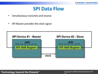
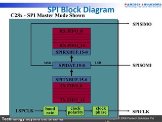
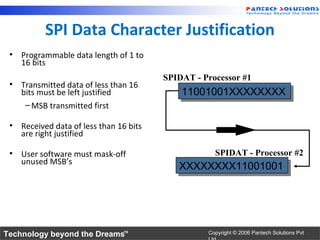
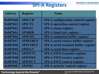
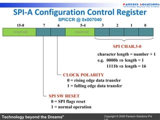
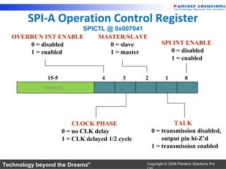
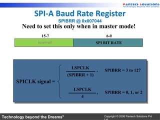
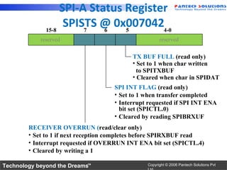
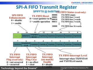
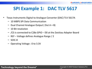
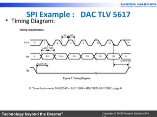
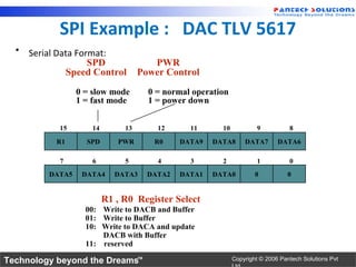
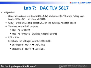
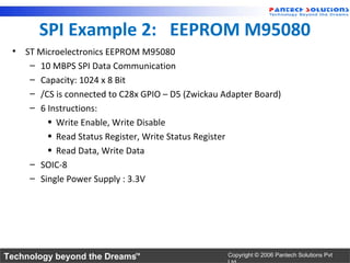
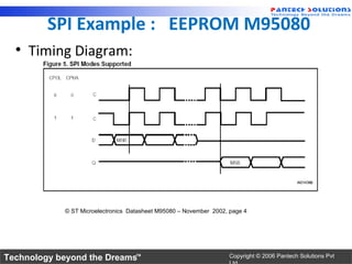

The document provides an overview of the Serial Peripheral Interface (SPI) for the TMS320F2812 digital signal controller, detailing its data flow, architecture, and operational registers. It explains the communication setup between master and slave devices, data length programmability, and configuration registers. Additionally, it includes examples of using the SPI interface with devices like the DAC TLV 5617 and EEPROM M95080, along with their respective operational commands and timing diagrams.