Download to read offline
![Area Optimization of SPI Module Using Verilog HDL
http://www.iaeme.com/IJECET/index.asp 39 editor@iaeme.com
1. INTRODUCTION
The communication links across components of a chip or a board may be either serial
or parallel. Serial communication is performed over fewer interconnecting cables,
thus enables to save a significant amount of space and reduce the number of
connecting pins. These reasons have led the serial communication interfaces to play a
major role in the field of embedded systems.
Even though serial communications like I2
C offers much more features than SPI,
Such as less pin count, automatic multi-master conflicts handling and built in
addressing management etc. SPI is preferable, since it is very simple, high speed
protocol, gives better throughput and offers extensions and variations.
Technology has been increased Integrated chips came into picture, where millions
of devices are integrated in to the single chip reduces area and Cost as well. In this
Paper we moved one more step to reduce area consumed by the SPI module.
SPI protocol introduced by the Motorola has four wires. It doesn’t have a Certain
Speed limit, today’s it works up to 10Mega bits per second. It is a Mater-Slave
protocol i.e., A Module can be acts as either Master or Slave. Master initiates the
transmission and sends out Clock.
In this paper we used a Structural code Verilog to implement SPI module. A
simple master, slave are deigned and the whole design is simulated and synthesized
using Xilinx9.1.
1.1. SPI Protocol
SPI is a simple four wire protocol designed by the Motorola initially, later many
vendors came up with new SPI designs ,some features added .it is a full duplex,
Synchronous serial comminution protocol. It isn’t a standard protocol like I2
C.
Designer has freedom to Extend it .SPI works in either master mode or Slave mode.
Four pins and their description according to the Motorola as below
Table1 Shows how the purpose of pins vary for master and slave modules
Pin notation Master Slave
MOSI (Master out slave in) Output pin Input pin
MISO (master in Slaveout) Input pin Output pin
SCK (serial clock) Output pin Input Pin
SS_ba (slave select) Output pin Input pin
Master starts sending or receiving by asserting slave select line of particular slave,
generates Clock and sends out the clock to the slave through SCK line, keep whole
transmission under control of the clock.
Every SPI module has mainly Port logic, Baud rate generation logic, Shift logic
[7]. It has 8 bit registers through which user can sets SPI module. Even it is 8 bit, it
can transmit up to 12 bits. Control word written decides whether the SPI Module
works as master or slave, the two shift register’s , one in Master and one in Slave are
Connected in loop through MOSI and MISO lines[7]. Since it is full duplex for every
clock pulse one bit is shifted in and shifted out of the module. Once Data has been
received, data will transfer to receive data register parallelly, sets bits in Status
register.](https://image.slidesharecdn.com/ijecet0703005-160729092313/85/AREA-OPTIMIZATION-OF-SPI-MODULE-USING-VERILOG-HDL-2-320.jpg)
![Bangaru Kalpana, Amrut Anilrao Purohit and R. Venkata Siva Reddy
http://www.iaeme.com/IJECET/index.asp 40 editor@iaeme.com
Baud rate register
R/W SPPR2 SPPR1 SPPR0 SPR2 SPR1 SPR0
Reset 0 0 0 0 0 0 0 0
Figure1 Reset values, bits description of baud rate register
Above shows a baud rate register with 8 bits sets the clock rate, SPPR2, SPPR1,
SPPR0 are Baud rate preselection bits and SPR0, SPR1, SPR2 SPI Baud rate selection
bits combinely to divide clock to desired frequency.
Status Register: As per name it shows the status of SPI module
R/W SPIF SPTEF
Reset 0 0 0 0 0 0 0 0
Figure2 Reset values and bit descriptions of status register
SPTEF -set's the interrupt when the transmit data register is empty. Clearing this
bit after writing to data register starts next transmission.
SPIF-SPI interrupt flag: Once data has been received, this bit is set. Reading data
register without reading status register is not allowed.
Control register
R/W SPIE SPE SPTIE MSTR CPOL CPHA SSOE LSBFE
Reset 0 0 0 0 1 0 0 0
Figure3: Reset values and bit descriptions of control register
SPIE- interrupt enable bit of SPI module. Enable the interrupt for reading
operation if SPIF =1.ISR interrupt service routine, which includes operations to Start
next byte of transmission consider the interrupt raises by SPIF this bit is to be set.
SPE- system enable bit of SPI module. SPI module works only, if this bit is set.
Clearing of this bit disables the SPI module and goes to idle state. SPTIE-Transmit
enable bit of SPI. Enable the interrupt for next transmission if SPITFE=1.This bit
enables the SPTEF interrupt to survive. MSTR-This bit shows weather module acts as
master or slave, if 1 acts as master. CPOL: Clock polarity bit, if 1, Clock inversion
occurs. This bit sets the clock as inverted clock or non-inverted that module has to
work. CPHA: This bit decides at which clock edges latching and shifting has to occur,
if it is 0, latching occurs on even edges and shifting in odd. SSOE: Slave select output
enabled, for master acts as output pin assert to Vcc if single master, for slave acts as
input pin grounded to 0 if single slave. LSBFE-This bit decides which bit to shift
either LSB (least significant bit) or MSB (most significant bit) to shift.
2. FUNCTIONAL DESCRIPTION
Control word written decides Module as a master or Slave. SPE bit enables the SPI
module and MSTR decides Mater or Slave [4].
MASTER
If MSTR=1, Module do master functions.it has to generate Clock. Baud logic
generates the clock from the word written to the baud rate register. Master initiates the
transmission by selecting slave through SS_bar line. The slave by asserting slave
select line of particular slave to 0 in Multi slave mode. If single slave in](https://image.slidesharecdn.com/ijecet0703005-160729092313/85/AREA-OPTIMIZATION-OF-SPI-MODULE-USING-VERILOG-HDL-3-320.jpg)
![Area Optimization of SPI Module Using Verilog HDL
http://www.iaeme.com/IJECET/index.asp 41 editor@iaeme.com
communication, VCC is given to SS pin. It begins transmission by reading the Status
register, if SPITE =1 write the data has to be transmitted into Transmit data register.
Transmit data register shifts 8bit data parrallely into Shift register by clearing SPITE
flag. Communication occurs by transmitting one bit per one clock pulse, after 8 pulses
data has been received shifted out parallelly into Receive data register by setting SPIF
flag.
Slave
If MSTR=0, module acts as Slave. In slave mode SCK and MOSI acts as input pins
and MISO as output pin by default. Select pin is connected to the ground before
transmission. Data exchanging occurs under the control of master clock. Once data
has been received, bits are transmitted to Data register by setting SPIF flag bit. This
bit is cleared by doing read accesses to the status register followed by data register.
2.1.1. Transmission Formats: [4]
CPOL, CPHA bits in the Control register decides four modes in which data
transmission occurs. CPOL bit decides, Clock is inverted or not.
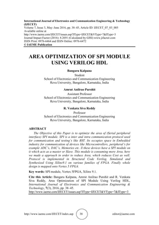
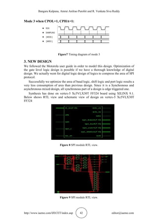
Mode 0 when CPOL=0, CPHA=0:
Data changing on falling edge, reading on raising edge
FIGURE 4 Timing diagram of mode0
Mode 1 when CPOL=1, CPHA=0:
FIGURE 5 Timing diagram of mode1
Mode 2 when CPOL=0, CPHA=1:
FIGURE 6 Timing diagram of mode2](https://image.slidesharecdn.com/ijecet0703005-160729092313/85/AREA-OPTIMIZATION-OF-SPI-MODULE-USING-VERILOG-HDL-4-320.jpg)
![Area Optimization of SPI Module Using Verilog HDL
http://www.iaeme.com/IJECET/index.asp 43 editor@iaeme.com
4. IMPLEMENTATION RESULTS
Whole design implemented in XILINX9.1. Below shows verification results of design
done by using MODELSIM 9.1. Design wrong with control, data, and baud registers
which has to set by the user. A default value has been assigned to the register before
module works for transmission. In our design default values are shown above.
Below shows synthesis results of design, mapped on to vertex-5 Xc5VLX30T
FF324 board, spatran3 board etc... A comparison is made to the previous design
results.
SPI master module sending data out:
Figure 10.SPI module as Master when MSTR=1.
SPI slave module receiving data:
Figure 11 SPI module as a slave when MSTR=0.
Table 2 Shows Synthesis results on Vertex 5 xc5vlx30-3ff324 comparison [1] & [4]
Used by Utilized in
Our design Available percentage
Slices count 0 40 0%
LUT count 40 19200 0%
Bound ed IOB ‘s 22 220 10%](https://image.slidesharecdn.com/ijecet0703005-160729092313/85/AREA-OPTIMIZATION-OF-SPI-MODULE-USING-VERILOG-HDL-6-320.jpg)
![Bangaru Kalpana, Amrut Anilrao Purohit and R. Venkata Siva Reddy
http://www.iaeme.com/IJECET/index.asp 44 editor@iaeme.com
Table3 Shows Synthesis results comparison on different boards with previous design done in
reference [2]
Spartan 3E Used by Used By previous
XC3S500E -
5[2]
Our design design Available
Slices count 13 51 4656
LUT count of
4 input
92 23 9312
Bounded
IOB’s 21outof232
22 Out of 92
Spartan 3E
XC3S1200E
-5
Slices count 13 51 8672
LUT count 23 92 17344
Bounded
IOB’s
22outof
190
21 out of
250
Virtex 4
XC4VFX100
-12
Slices
count
13 43 42176
LUT count 81 23 84352
Bounded
IOB’s
22 out of
576
21out of
680
5. CONCLUSION AND FUTURE SCOPE
Proposed design is simple SPI module acts as either master or slave. Our design
consumes less area comparatively known from results in section before. Reducing
area, reduces cost of design as well. Future, by adding some more features this
module can also work in multi slave and multi master communication environment,
still consumes less area.
REFERENCES
[1] Anand N, George Joseph, Suwin Sam Oommen, and R Dhanabal, design and
implementation of high speed serial interface, School of Electronics Engineering,
VIT University, Vellore, India.
[2] Amit Kumar Shrivastava and Himanshu Joshi, Design, Implementation and
Functional Verification of Serial Communication Protocols (SPI and I2C) on
FPGAs, HCTL Open IJTIR Volume 4, July 2013.](https://image.slidesharecdn.com/ijecet0703005-160729092313/85/AREA-OPTIMIZATION-OF-SPI-MODULE-USING-VERILOG-HDL-7-320.jpg)
![Area Optimization of SPI Module Using Verilog HDL
http://www.iaeme.com/IJECET/index.asp 45 editor@iaeme.com
[3] T. Durga Prasad and B. Ramesh Babu, Design and simulation of master/ using
Verilog HDL, IJSR, 3 (8), August 2014.
[4] Prof. Jai Karan Singh and Prof. Mukesh Tiwari, Implementation of SPI slave on
FPGA, IJAET/Vol.III/ Issue IV/Oct.-Dec, 2012/24-26.
[5] A.K. Oudjida et al, FPGA Implementation of I2C and SPI protocols, IEEE
Instrumentation & Measurement Magazine, pp.8–13, February 2009.
[6] Motorola Inc, SPI Block Guide V03.06, February 2003.
[7] Fareha Naqvi, design and implementation of serial peripheral interface protocol
Using Verilog HDL, 2015 IJEDR, 3(3) ISDSN: 2321–9939.
[8] Qazi Raza Abdul Quadir, Arif Rasool, Manan Mushtaq and Yasirbhat, Design
and Simulation of A Non-Pipelined, Multi- Cycle 16 Bit Risc Educational
Processor Using Verilog HDL, International Journal of Electronics and
Communication Engineering & Technology, 5(9), 2014, pp. 14–23.
[9] Md. Ajmal Sadiq, T.Naga Raju and Kumar. Keshamoni, Modeling and
Simulation Of Test Data Compression Using Verilog, International Journal of
Electronics and Communication Engineering & Technology, 4(5), 2013, pp. 143–
141.
[10] R.Kathiresan, M.Thangavel, K.Rathinakumar And S.Maragadharaj, Analysis of
Different Bit Carry Look Ahead Adder Using Verilog Code, International
Journal of Electronics and Communication Engineering & Technology, 4(4),
2013, pp. 214–220.](https://image.slidesharecdn.com/ijecet0703005-160729092313/85/AREA-OPTIMIZATION-OF-SPI-MODULE-USING-VERILOG-HDL-8-320.jpg)

This paper discusses the optimization of the Serial Peripheral Interface (SPI) module using Verilog HDL to reduce area consumption in FPGA designs. The authors implemented the SPI protocol in structural Verilog and performed simulations and synthesis using Xilinx tools, achieving significant area reductions compared to previous designs. The study concludes that a smaller area also decreases overall costs, with potential future developments to enhance functionality for multi-master and multi-slave environments.