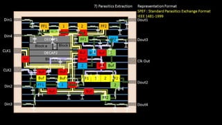
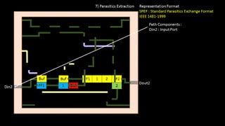
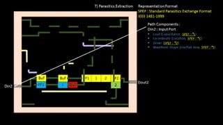
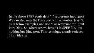
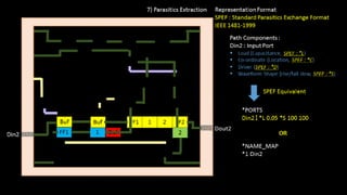
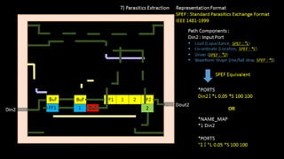
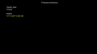
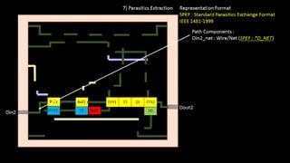
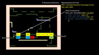
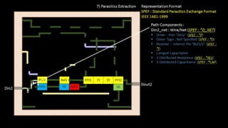
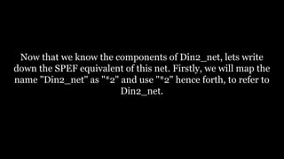
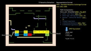
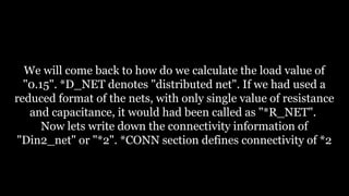
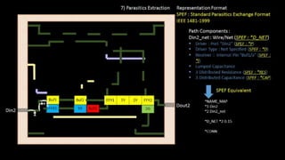
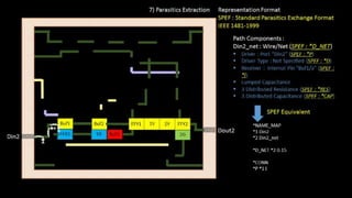
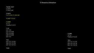
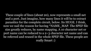
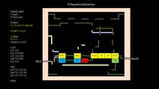
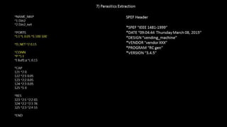
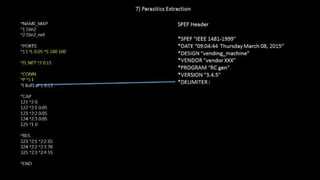
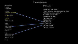
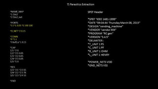
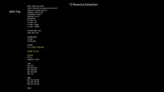
So, this has been due for long time. May be because of tight tape out deadlines, this very important piece of Physical Design flow just got missed. And I am sure, like me, many might be curious to know what is the IEEE SPEF format, what does various attributes of SPEF file represent, etc...
The paper describes the basic of Timing analysis like setup time, hold time, delays in logic circuits, timing violations and different types of timing paths like flip-flop to flip-flop path, clock gating path, asynchronous signal path, half cycle path, flip-flop to output path, input to flip-flop path and input to output path.
Note : To get more understanding Recommending to see first section - Low power in vlsi with upf basics part 1
With Increase in Portable devices, VLSI chips has to consider about Power usages in VLSI silicon chips. So Power Aware design and verification is so important in Industry. To get basic knowledge on Low Power Design and Verification with UPF basics Go through this Slides.
Clock Tree Synthesis is a technique for distributing the clock equally among all sequential parts of a VLSI design. The purpose of Clock Tree Synthesis is to reduce skew and delay. Clock Tree Synthesis is provided the placement data as well as the clock tree limitations as input. Clock Tree Synthesis (CTS) is the technique of balancing the clock delay to all clock inputs by inserting buffers/inverters along the clock routes of an ASIC design. As a result, CTS is used to balance the skew and reduce insertion latency. Before Clock Tree Synthesis, all clock pins were driven by a single clock source. Clock tree synthesis includes both clock tree construction and clock tree balance. Clock tree inverters may be used to create a clock tree that maintains the correct transition (duty cycle), and clock tree buffers (CTB) can balance the clock tree to fulfil the skew and latency requirements. To fulfil the space and power limits, fewer clock tree inverters and buffers should be employed.
Timing and Design Closure in Physical Design Flows Olivier Coudert
A physical design flow consists of producing a production-worthy layout from a gate-level netlist subject to a set of constraints. We focus on the problems imposed by shrinking process technologies. It exposes the problems of timing closure, signal integrity, design variable dependencies, clock and power/ground routing, and design signoff. It also surveys some physical design flows, and outlines a refinement-based flow.
This is the presentation that was shared by Nilesh Ranpura and Vineeth Mathramkote at CDNLIVE 2015. The session briefs about the implementation challenges and covers the solution approach and how to achieve results
https://www.udemy.com/vlsi-academy
Usually, while drawing any circuit on paper, we have only one 'vdd' at the top and one 'vss' at the bottom. But on a chip, it becomes necessary to have a grid structure of power, with more than one 'vdd' and 'vss'. The concept of power grid structure would be uploaded soon. It is actually the scaling trend that drives chip designers for power grid structure.
With Increase in Portable devices, VLSI chips has to consider about Power usages in VLSI silicon chips. So Power Aware design and verification is so important in Industry. To get basic knowledge on Low Power Design and Verification with UPF basics Go through this Slides.
VLSI Physical Design Flow(http://www.vlsisystemdesign.com)VLSI SYSTEM Design
Learning becomes Fun..
When tedious & difficult topics like Chip Design are explained in simple n creative videos....https://www.udemy.com/vlsi-academy
A typical design flow follows the below structure and can be broken down into multiple steps. Some of these phases happen in parallel and some in sequentially.
Requirements
A customer of a semiconductor firm is typically some other company who plans to use the chip in its systems or end products. So, the customer's requirements also play an important role in deciding how the chip should be designed.
The first step is to collect the requirements, estimate the end product's market value, and evaluate the number of resources required to do the project.
Specifications
The next step is to collect specifications that describe the functionality, interface abstractly, and over all architecture of the chip to be designed. This can be something along the lines such as:
Play
Next
Unmute
Current TimeÂ
0:00
/
DurationÂ
18:10
Â
Fullscreen
Backward Skip 10s
Play Video
Forward Skip 10s
Requires computational power to run imaging algorithms to support virtual reality.
Requires two ARM A53 processors with coherent interconnect and should run at 600 MHz.
Requires USB 3.0, Bluetooth, and PCIe 2nd gen interfaces.
It should support 1920x1080 pixel displays with an appropriate controller.
Digital Design
Because of the complex nature of modern chips, it's impossible to build something from scratch, and in many cases, many components will be reused.
For example, company A requires a FlexCAN module to interact with other modules in an automobile. They can either buy the FlexCAN design from another company to save time and effort or spend resources to build one.
It's not practical to design such a system from basic building blocks such as flip-flops and CMOS transistors.
Instead, a behavioral description is developed to analyze the design in terms of functionality, performance, and other high-level issues using a Hardware Description Language such as Verilog or VHDL.
This is usually done by a digital designer and is similar to a high-level computer programmer equipped with digital electronics skills.
Verification
Once the RTL design is ready, it needs to be verified for functional correctness.
For example, a DSP processor is expected to issue bus transactions with fetching instructions from memory and know that this will happen as expected.
The functional verification is required at this point, which is done with EDA simulators' help that can model the design and apply a different stimulus to it. This is the job of a pre-silicon verification engineer.
Logic Synthesis
Now we will convert this design into hardware schematic with real elements such as combinational gates and flip-flops. This step is called synthesis.
Logic synthesis tools enable the conversion of RTL description in HDL to a gate-level netlist. This netlist is a description of the circuit in terms of gates and connections between them.
Logic synthesis tools ensure that the netlist meets timing, area, and power specifications. Typically, they have access to different technology node
This presentation includes basic information related to sockets ,socket-buffer,cliet-server programs and relationship between them
The files included in the ppt for the variables are taken from linux-2.6.10.
In case of any queriers.
contact souravpunoriyar@gmail.com
Project descriptionIn this Phase, we will develop two nodes.docxwkyra78
Project description:
In this Phase, we will develop two nodes for the network simulator. The first node is a trasmitter and the second node is a receiver.
Each node is defined by a unique node_ID. That is, there are no two nodes in the network with the same ID.
Since we are using a single machine to perform PHY transmissions, the node_ID values can be arbitrary IP address.
Each node has five layers namely: application_layer, transport_layer, network_layer, link_layer and PHY_layer.
For this phase of the project, we develop protocols for three layers: application_layer, transport_layer and PHY_layer
Each layer (depending on its location) has allocated buffers to establish communication with the other layers above or below it.
For instance, the transport_layer has four buffers: to_network_layer, from_network_layer, from_application_layer, to_application_layer
For the application_layer, we will develop file transfer protocol (FTP). The FTP class has two sides, the transmitter and receiver sides.
The transmitter sides reads a file (specified by user) and convert that into application_layer_messages.
The receiver side gets application_layer_messages from the transport_layer converts them into single file.
For the transport_layer, we will develop UDP protocol. This protocol has two sides, the transmitter and receiver sides.
The transmitter side gets the application_layer_messages from the application_layer and converts them into transport_layer segments.
Note that the length of each segment should be maximum segment size MSS (excluding UDP header).
The value of MSS usually depends on the PHY link that each node is connected to.
Each segment should have the following fields:
# application_layer_messages_no: 4bytes: 32 bits
# segment_no: packet number : 4bytes: 32 bits
# source_port: this field identifies the sender's port : 2 bytes: 16 bits
# destination_port: This field identifies the receiver's port: 2 bytes : 16 bits
# Length: the length in bytes of the UDP header and UDP data : 2 bytes : 16 bits
# Checksum: the checksum field is used for error-checking of the header and data. 2 bytes : 16 bits
# Reference flag: indicates the beginning of a set of segments for an individual application message
It is important to note that each application_layer_messages is divided to a set of segments. The reference byte represent the beginning of each set.
The receiver side of the transport_layer gets the set of segments and concatenated them to makes a single application_layer_messages.
For the PHY layer, we use python socket library to send and receive messages over ports.
This is because, we will use a single machine for the network simulator.
The PHY sender simply transfers packets over the specified port.
The PHY receiver listens to that port and send the received packets to the upper layer.
For this Phase, you need to develop the following files:
application_lay ...
Difference between OSI Layer & TCP/IP LayerNetwax Lab
Difference between OSI Layer & TCP/IP Layer
TCP/IP OSI
It has 4 layers. It has 7 layers.
TCP/IP Protocols are considered to be standards
around which the internet has developed.
OSI Model however is a "generic, protocolindependent standard."
Follows Vertical Approach Follows Horizontal Approach
In TCP/IP Model, Transport Layer does not
Guarantees delivery of packets.
In OSI Model, Transport Layer Guarantees
delivery of packets.
I have been receiving multiple queries on what is clk-to-q delay, how's it different from library setup time and library hold time, etc. I mentioned in my discussions, that the videos on CMOS digital circuit will be uploaded soon, but looks like, it might take some time, and hence decided to uploaded few images from my CMOS course, to explain the difference between all of them.
https://www.udemy.com/vlsi-academy
http://vlsisystemdesign.com/need_for_decap.php
A decoupling capacitor is a capacitor, which is used decouple the critical cells from main power supply, in order to protect the cells from the disturbance occuring in the power distribution lines and source. The purpose of using decoupling capacitors is to deliver current to the gates during switching. Herein, we would peep inside the reasons for the distrubance occuring in the power distribution lines.
https://www.udemy.com/vlsi-academy
http://vlsisystemdesign.com/switchAct.php
A CMOS, is basically an inverter logic (NOT gate), that consists of a PMOS at the top, and NMOS at the bottom (as shown in figure below), whose 'gate' and 'drain' terminal are tied together. The 'gate' terminals of both the MOS transistors is the input side of an inverter, whereas, the 'drain' terminals form the output side.
https://www.udemy.com/vlsi-academy
http://vlsisystemdesign.com/noise_margin.php
Noise margin is the amount of noise that a CMOS circuit could withstand without compromising the operation of circuit. Noise margin does makes sure that any signal which is logic '1' with finite noise added to it, is still recognised as logic '1' and not logic '0'. It is basically the difference between signal value and the nosie value.
https://www.udemy.com/vlsi-academy
http://vlsisystemdesign.com/place_decap.php
Once the critical cells are placed on the chip, it becomes necessary to surround the critical cells by decoupling capacitors. The placement of de-coupling capacitors surrounding the pre-placed cells improves the reliability and efficiency of the chip.
Floorplan (http://www.vlsisystemdesign.com/PD-Flow.php)VLSI SYSTEM Design
https://www.udemy.com/vlsi-academy
Floorplanning is basically the arrangement of logical blocks (i.e. multiplexer, AND, OR gates, buffers) on silicon chip.
Define location of Preplaced cells(http://www.vlsisystemdesign.com/PD-Flow.php)VLSI SYSTEM Design
https://www.udemy.com/vlsi-academy
During placement and routing, most of the placement tools, place/move logic cells based on floorplan specifications. Some of the important or critical cell's locations has to be pre-defined before actual placement and routing stages. The critical cells are mostly the cells related to clocks, viz. clock buffers, clock mux, etc. and also few other cells such as RAM's, ROM,s etc. Since, these cells are placed in to core before placement and routing stage, they are called 'preplaced cells'.
Define Width and Height of Core and Die (http://www.vlsisystemdesign.com/PD-F...VLSI SYSTEM Design
https://www.udemy.com/vlsi-academy
The very first step in chip design is floorplanning, in which the width and height of the chip, basically the area of the chip, is defined. A chip consists of two parts, 'core' and 'die'.
Connector Corner: Automate dynamic content and events by pushing a buttonDianaGray10
Here is something new! In our next Connector Corner webinar, we will demonstrate how you can use a single workflow to:
Create a campaign using Mailchimp with merge tags/fields
Send an interactive Slack channel message (using buttons)
Have the message received by managers and peers along with a test email for review
But there’s more:
In a second workflow supporting the same use case, you’ll see:
Your campaign sent to target colleagues for approval
If the “Approve” button is clicked, a Jira/Zendesk ticket is created for the marketing design team
But—if the “Reject” button is pushed, colleagues will be alerted via Slack message
Join us to learn more about this new, human-in-the-loop capability, brought to you by Integration Service connectors.
And...
Speakers:
Akshay Agnihotri, Product Manager
Charlie Greenberg, Host
LF Energy Webinar: Electrical Grid Modelling and Simulation Through PowSyBl -...DanBrown980551
Do you want to learn how to model and simulate an electrical network from scratch in under an hour?
Then welcome to this PowSyBl workshop, hosted by Rte, the French Transmission System Operator (TSO)!
During the webinar, you will discover the PowSyBl ecosystem as well as handle and study an electrical network through an interactive Python notebook.
PowSyBl is an open source project hosted by LF Energy, which offers a comprehensive set of features for electrical grid modelling and simulation. Among other advanced features, PowSyBl provides:
- A fully editable and extendable library for grid component modelling;
- Visualization tools to display your network;
- Grid simulation tools, such as power flows, security analyses (with or without remedial actions) and sensitivity analyses;
The framework is mostly written in Java, with a Python binding so that Python developers can access PowSyBl functionalities as well.
What you will learn during the webinar:
- For beginners: discover PowSyBl's functionalities through a quick general presentation and the notebook, without needing any expert coding skills;
- For advanced developers: master the skills to efficiently apply PowSyBl functionalities to your real-world scenarios.
Software Delivery At the Speed of AI: Inflectra Invests In AI-Powered QualityInflectra
In this insightful webinar, Inflectra explores how artificial intelligence (AI) is transforming software development and testing. Discover how AI-powered tools are revolutionizing every stage of the software development lifecycle (SDLC), from design and prototyping to testing, deployment, and monitoring.
Learn about:
• The Future of Testing: How AI is shifting testing towards verification, analysis, and higher-level skills, while reducing repetitive tasks.
• Test Automation: How AI-powered test case generation, optimization, and self-healing tests are making testing more efficient and effective.
• Visual Testing: Explore the emerging capabilities of AI in visual testing and how it's set to revolutionize UI verification.
• Inflectra's AI Solutions: See demonstrations of Inflectra's cutting-edge AI tools like the ChatGPT plugin and Azure Open AI platform, designed to streamline your testing process.
Whether you're a developer, tester, or QA professional, this webinar will give you valuable insights into how AI is shaping the future of software delivery.
Neuro-symbolic is not enough, we need neuro-*semantic*Frank van Harmelen
Neuro-symbolic (NeSy) AI is on the rise. However, simply machine learning on just any symbolic structure is not sufficient to really harvest the gains of NeSy. These will only be gained when the symbolic structures have an actual semantics. I give an operational definition of semantics as “predictable inference”.
All of this illustrated with link prediction over knowledge graphs, but the argument is general.
Dev Dives: Train smarter, not harder – active learning and UiPath LLMs for do...UiPathCommunity
💥 Speed, accuracy, and scaling – discover the superpowers of GenAI in action with UiPath Document Understanding and Communications Mining™:
See how to accelerate model training and optimize model performance with active learning
Learn about the latest enhancements to out-of-the-box document processing – with little to no training required
Get an exclusive demo of the new family of UiPath LLMs – GenAI models specialized for processing different types of documents and messages
This is a hands-on session specifically designed for automation developers and AI enthusiasts seeking to enhance their knowledge in leveraging the latest intelligent document processing capabilities offered by UiPath.
Speakers:
👨🏫 Andras Palfi, Senior Product Manager, UiPath
👩🏫 Lenka Dulovicova, Product Program Manager, UiPath
Builder.ai Founder Sachin Dev Duggal's Strategic Approach to Create an Innova...Ramesh Iyer
In today's fast-changing business world, Companies that adapt and embrace new ideas often need help to keep up with the competition. However, fostering a culture of innovation takes much work. It takes vision, leadership and willingness to take risks in the right proportion. Sachin Dev Duggal, co-founder of Builder.ai, has perfected the art of this balance, creating a company culture where creativity and growth are nurtured at each stage.
Let's dive deeper into the world of ODC! Ricardo Alves (OutSystems) will join us to tell all about the new Data Fabric. After that, Sezen de Bruijn (OutSystems) will get into the details on how to best design a sturdy architecture within ODC.
Slack (or Teams) Automation for Bonterra Impact Management (fka Social Soluti...Jeffrey Haguewood
Sidekick Solutions uses Bonterra Impact Management (fka Social Solutions Apricot) and automation solutions to integrate data for business workflows.
We believe integration and automation are essential to user experience and the promise of efficient work through technology. Automation is the critical ingredient to realizing that full vision. We develop integration products and services for Bonterra Case Management software to support the deployment of automations for a variety of use cases.
This video focuses on the notifications, alerts, and approval requests using Slack for Bonterra Impact Management. The solutions covered in this webinar can also be deployed for Microsoft Teams.
Interested in deploying notification automations for Bonterra Impact Management? Contact us at sales@sidekicksolutionsllc.com to discuss next steps.
Accelerate your Kubernetes clusters with Varnish CachingThijs Feryn
A presentation about the usage and availability of Varnish on Kubernetes. This talk explores the capabilities of Varnish caching and shows how to use the Varnish Helm chart to deploy it to Kubernetes.
This presentation was delivered at K8SUG Singapore. See https://feryn.eu/presentations/accelerate-your-kubernetes-clusters-with-varnish-caching-k8sug-singapore-28-2024 for more details.
JMeter webinar - integration with InfluxDB and GrafanaRTTS
Watch this recorded webinar about real-time monitoring of application performance. See how to integrate Apache JMeter, the open-source leader in performance testing, with InfluxDB, the open-source time-series database, and Grafana, the open-source analytics and visualization application.
In this webinar, we will review the benefits of leveraging InfluxDB and Grafana when executing load tests and demonstrate how these tools are used to visualize performance metrics.
Length: 30 minutes
Session Overview
-------------------------------------------
During this webinar, we will cover the following topics while demonstrating the integrations of JMeter, InfluxDB and Grafana:
- What out-of-the-box solutions are available for real-time monitoring JMeter tests?
- What are the benefits of integrating InfluxDB and Grafana into the load testing stack?
- Which features are provided by Grafana?
- Demonstration of InfluxDB and Grafana using a practice web application
To view the webinar recording, go to:
https://www.rttsweb.com/jmeter-integration-webinar
State of ICS and IoT Cyber Threat Landscape Report 2024 previewPrayukth K V
The IoT and OT threat landscape report has been prepared by the Threat Research Team at Sectrio using data from Sectrio, cyber threat intelligence farming facilities spread across over 85 cities around the world. In addition, Sectrio also runs AI-based advanced threat and payload engagement facilities that serve as sinks to attract and engage sophisticated threat actors, and newer malware including new variants and latent threats that are at an earlier stage of development.
The latest edition of the OT/ICS and IoT security Threat Landscape Report 2024 also covers:
State of global ICS asset and network exposure
Sectoral targets and attacks as well as the cost of ransom
Global APT activity, AI usage, actor and tactic profiles, and implications
Rise in volumes of AI-powered cyberattacks
Major cyber events in 2024
Malware and malicious payload trends
Cyberattack types and targets
Vulnerability exploit attempts on CVEs
Attacks on counties – USA
Expansion of bot farms – how, where, and why
In-depth analysis of the cyber threat landscape across North America, South America, Europe, APAC, and the Middle East
Why are attacks on smart factories rising?
Cyber risk predictions
Axis of attacks – Europe
Systemic attacks in the Middle East
Download the full report from here:
https://sectrio.com/resources/ot-threat-landscape-reports/sectrio-releases-ot-ics-and-iot-security-threat-landscape-report-2024/
DevOps and Testing slides at DASA ConnectKari Kakkonen
My and Rik Marselis slides at 30.5.2024 DASA Connect conference. We discuss about what is testing, then what is agile testing and finally what is Testing in DevOps. Finally we had lovely workshop with the participants trying to find out different ways to think about quality and testing in different parts of the DevOps infinity loop.
2. So, this has been due for long time. May be
because of tight tape out deadlines, this very
important piece of Physical Design flow just got
missed. And I am sure, like me, many might be
curious to know what is the IEEE SPEF format,
what does various attributes of SPEF file
represent, etc...
3. So, here you go. Finally got time to
make video on IEEE SPEF format. Let's nail
this down, with below example design, which I
have been using on Udemy
4.
5. We will take a piece of the circuit and write the
SPEF file for a piece of input port and net
6.
7. Let's write down the path components of Input
port Din2 in SPEF format, which will also be a
part of large SPEF file
8.
9.
10.
11. In the above SPEF equivalent "I" represents input port
We can also map the Din2 port with a number, (say *1,
as in below example), and use *1 as reference for Input
Port Din2. So, wherever, we have *1 in SPEF file, it is
nothing but Din2 port. This technique greatly reduces
SPEF file size
16. Further, we will extract the net
connected to Din2 (shown below) and
write a SPEF format of the same
17.
18. Let's move on with identifying the
path components of net connected to
Din2 port shown below
19.
20. For now, let's have a distributed RC network representation of
the net (shown below). We do have another way of
representing RC network in reduced format. I will come back
to that in a moment
21.
22. Now that we know the components of Din2_net, lets write
down the SPEF equivalent of this net. Firstly, we will map the
name "Din2_net" as "*2" and use "*2" hence forth, to refer to
Din2_net.
23.
24. We will come back to how do we calculate the load value of
"0.15". *D_NET denotes "distributed net". If we had used a
reduced format of the nets, with only single value of resistance
and capacitance, it would had been called as "*R_NET".
Now lets write down the connectivity information of
"Din2_net" or "*2". *CONN section defines connectivity of *2
25.
26. The below says. *2 (Din2_net) is connected to external port
(*P), named *1 (port Din2), which has direction "input" (I)
27.
28. The other end of net "*2" is connected to internal pin "Buf1:a"
and having a load (*L) of 0.15 units. I will come back later on
the "units" section, in my following post
29.
30. This becomes a part of the SPEF file, so lets put it in a file, that
we were maintaining from last post
31.
32. Notice, we have 3 capacitances and 3 resistances on the net. So
the way to represent them is in below image. The numbers
"121", "122", etc. are the line numbers, *2:1, *2:2.... are the
respective capacitances. I will get back on *2 and *1 and the
beginning and end of the cap section. Broadly, this is to denote
the start and end section of *CAP
33.
34. Now, we have 4 nodes, and within a pair of node, we have a
resistance, like below
35.
36. With the introduction of nodes, the representation of
resistance has now become fairly simple, like below
37.
38. These set of lines for distributed resistance and capacitance,
will become a part of the SPEF file, we were maintaining. So
let;s add it there
39.
40. These couple of lines (about 20), now represents a small net
and a port. Just imagine, how many lines it will be to extract
parasitics for the complete circuit, below. Its HUGE. I think,
now we nail the reason for having *NAME_MAP. The SPEF file
size greatly reduces, by name mapping. A 10 character net or
port name can be reduced to a 2~3 character net name and can
be referred and reused in the whole SPEF file. These people are
really Smart :)
41.
42. Remember, I had mentioned, I will get back on units. So here
we go. We have a header file that defines all of the them.
Firstly, the design name, vendor name, version, etc.
43.
44. Then, the delimiter. Usually, in any report, we see, it as "/". In
SPEF you can have your own delimiter, by defining something
like below
49. Below is the SPEF file, for one net and one port
50.
51. So, next time, when you look at the SPEF, just make sure to
open it, and see, if what we discussed in all SPEF format posts,
does make sense.
And, In Lady Windemere's Fan, Oscar Wilde had Lord
Darlington quip that a cynic was 'a man who knows the
price of everything and the value of nothing.'
Let's value SPEF files :)
52. For more, please refer to below courses
Circuit design & SPICE simulations
https://www.udemy.com/vlsi-academy-circuit-design/?couponCode=forSlideshare
Physical design flow
https://www.udemy.com/vlsi-academy-physical-design-flow/?couponCode=forSlideshare
Clock tree synthesis
https://www.udemy.com/vlsi-academy-clock-tree-synthesis/?couponCode=forSlideshare
Signal integrity
https://www.udemy.com/vlsi-academy-crosstalk/?couponCode=forSlideshare
VLSI – Essential concepts and detailed interview guide
https://www.udemy.com/vlsi-academy/?couponCode=forSlideshare