Special Diode Types
Dr. Varun Kumar
Dr. Varun Kumar (IIIT Surat) Unit 1 1 / 11
Outlines
1 Varactors
2 Schottky-Barrier Diode
3 Photodiodes
PIN photodiode
Avalanche photodiode
4 Light-Emitting Diodes
Dr. Varun Kumar (IIIT Surat) Unit 1 2 / 11
Varactor diode:
Key properties of Varactor diode
The varactor diode is also known as
Variable capacitance diode
Variable reactance diode
Tuning diode
Varactor diode always function in reverse biasing condition.
Mathematical, formulation of capacitance can be expressed as
C =
0r A
d
and V =
Q
C
Its doping level is high.
⇒ Junction width reduces by increasing the doping concentration.
⇒ Higher the reverse voltage, greater be the junction width.
⇒ By changing the applied voltage the capacitance can be varied.
Dr. Varun Kumar (IIIT Surat) Unit 1 3 / 11
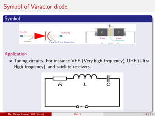
Symbol of Varactor diode
Symbol
Application
Tuning circuits. For instance VHF (Very high frequency), UHF (Ultra
High frequency), and satellite receivers.
Dr. Varun Kumar (IIIT Surat) Unit 1 4 / 11
Schottky-Barrier Diode
Schottky Diode
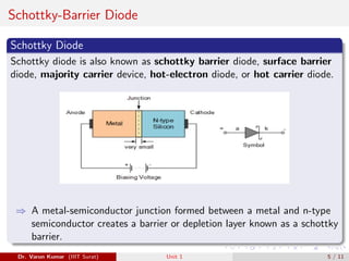
Schottky diode is also known as schottky barrier diode, surface barrier
diode, majority carrier device, hot-electron diode, or hot carrier diode.
⇒ A metal-semiconductor junction formed between a metal and n-type
semiconductor creates a barrier or depletion layer known as a schottky
barrier.
Dr. Varun Kumar (IIIT Surat) Unit 1 5 / 11
Continued–
⇒ A Schottky Diode is a metal-semiconductor diode with a low forward
voltage drop (0.2V-0.5V), pn-junction diode ∼ (0.6V-0.8V)

and a
very fast switching speed.
⇒ Barrier height depends on the combination of semiconductor and
metal.
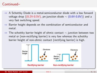
⇒ The schottky barrier height of ohmic contact ∼ junction between two
metal or (non-rectifying barrier) is very low whereas the schottky
barrier height of non-ohmic contact (rectifying barrier) is high.
Dr. Varun Kumar (IIIT Surat) Unit 1 6 / 11
Application of Schottky diode
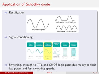
⇒ Rectification
⇒ Signal conditioning
⇒ Switching, through to TTL and CMOS logic gates due mainly to their
low power and fast switching speeds.
.
Dr. Varun Kumar (IIIT Surat) Unit 1 7 / 11
Photodiode
⇒ It is a form of light sensor that converts light energy into electrical
energy (voltage or current).
⇒ Between the p (positive) and n (negative) layers, an intrinsic layer is
present.
Types of photodiode:
1 PIN Photodiode
2 Avalanche Photodiode
Dr. Varun Kumar (IIIT Surat) Unit 1 8 / 11
Advantages and Disadvantages of PIN/Avalanche photodiode
Advantage of PIN photodiode
High-frequency response.
It is inexpensive and the response time is in nanoseconds.
PIN diodes have a broad spectral response.
Used for detection of laser pulses in ultra-fast switching circuits.
Disadvantage of PIN photodiode
It requires large reverse bias for its operation which reduces the SNR.
Advantages and Disadvantages of Avalanche Photodiode
⇒ It can detect very weak signal due to high current-gain bandwidth
product.
⇒ The construction is quite complicated.
Application: It is widely used in fibre optic communication Systems.
Dr. Varun Kumar (IIIT Surat) Unit 1 9 / 11
Light Emitting Diode (LED)
⇒ A light-emitting diode (LED) is a semiconductor light source that
emits light when current flows through it.
Dr. Varun Kumar (IIIT Surat) Unit 1 10 / 11
References
A. S. Sedra, D. E. A. S. Sedra, K. C. Smith et al., Microelectronic circuits. New
York: Oxford University Press, 1998.
R. L. Boylestad, Electronic devices and circuit theory. Pearson Education India,
2009.
D. L. Schilling, C. Belove, T. Apelewicz, and R. J. Saccardi, Electronic circuits:
discrete and integrated. McGraw-Hill Kogakushaˆ eTokyo Tokyo, 1968.
Dr. Varun Kumar (IIIT Surat) Unit 1 11 / 11

Special type diode

  • 1.
    Special Diode Types Dr.Varun Kumar Dr. Varun Kumar (IIIT Surat) Unit 1 1 / 11
  • 2.
    Outlines 1 Varactors 2 Schottky-BarrierDiode 3 Photodiodes PIN photodiode Avalanche photodiode 4 Light-Emitting Diodes Dr. Varun Kumar (IIIT Surat) Unit 1 2 / 11
  • 3.
    Varactor diode: Key propertiesof Varactor diode The varactor diode is also known as Variable capacitance diode Variable reactance diode Tuning diode Varactor diode always function in reverse biasing condition. Mathematical, formulation of capacitance can be expressed as C = 0r A d and V = Q C Its doping level is high. ⇒ Junction width reduces by increasing the doping concentration. ⇒ Higher the reverse voltage, greater be the junction width. ⇒ By changing the applied voltage the capacitance can be varied. Dr. Varun Kumar (IIIT Surat) Unit 1 3 / 11
  • 4.
    Symbol of Varactordiode Symbol Application Tuning circuits. For instance VHF (Very high frequency), UHF (Ultra High frequency), and satellite receivers. Dr. Varun Kumar (IIIT Surat) Unit 1 4 / 11
  • 5.
    Schottky-Barrier Diode Schottky Diode Schottkydiode is also known as schottky barrier diode, surface barrier diode, majority carrier device, hot-electron diode, or hot carrier diode. ⇒ A metal-semiconductor junction formed between a metal and n-type semiconductor creates a barrier or depletion layer known as a schottky barrier. Dr. Varun Kumar (IIIT Surat) Unit 1 5 / 11
  • 6.
    Continued– ⇒ A SchottkyDiode is a metal-semiconductor diode with a low forward voltage drop (0.2V-0.5V), pn-junction diode ∼ (0.6V-0.8V) and a very fast switching speed. ⇒ Barrier height depends on the combination of semiconductor and metal. ⇒ The schottky barrier height of ohmic contact ∼ junction between two metal or (non-rectifying barrier) is very low whereas the schottky barrier height of non-ohmic contact (rectifying barrier) is high. Dr. Varun Kumar (IIIT Surat) Unit 1 6 / 11
  • 7.
    Application of Schottkydiode ⇒ Rectification ⇒ Signal conditioning ⇒ Switching, through to TTL and CMOS logic gates due mainly to their low power and fast switching speeds. . Dr. Varun Kumar (IIIT Surat) Unit 1 7 / 11
  • 8.
    Photodiode ⇒ It isa form of light sensor that converts light energy into electrical energy (voltage or current). ⇒ Between the p (positive) and n (negative) layers, an intrinsic layer is present. Types of photodiode: 1 PIN Photodiode 2 Avalanche Photodiode Dr. Varun Kumar (IIIT Surat) Unit 1 8 / 11
  • 9.
    Advantages and Disadvantagesof PIN/Avalanche photodiode Advantage of PIN photodiode High-frequency response. It is inexpensive and the response time is in nanoseconds. PIN diodes have a broad spectral response. Used for detection of laser pulses in ultra-fast switching circuits. Disadvantage of PIN photodiode It requires large reverse bias for its operation which reduces the SNR. Advantages and Disadvantages of Avalanche Photodiode ⇒ It can detect very weak signal due to high current-gain bandwidth product. ⇒ The construction is quite complicated. Application: It is widely used in fibre optic communication Systems. Dr. Varun Kumar (IIIT Surat) Unit 1 9 / 11
  • 10.
    Light Emitting Diode(LED) ⇒ A light-emitting diode (LED) is a semiconductor light source that emits light when current flows through it. Dr. Varun Kumar (IIIT Surat) Unit 1 10 / 11
  • 11.
    References A. S. Sedra,D. E. A. S. Sedra, K. C. Smith et al., Microelectronic circuits. New York: Oxford University Press, 1998. R. L. Boylestad, Electronic devices and circuit theory. Pearson Education India, 2009. D. L. Schilling, C. Belove, T. Apelewicz, and R. J. Saccardi, Electronic circuits: discrete and integrated. McGraw-Hill Kogakushaˆ eTokyo Tokyo, 1968. Dr. Varun Kumar (IIIT Surat) Unit 1 11 / 11