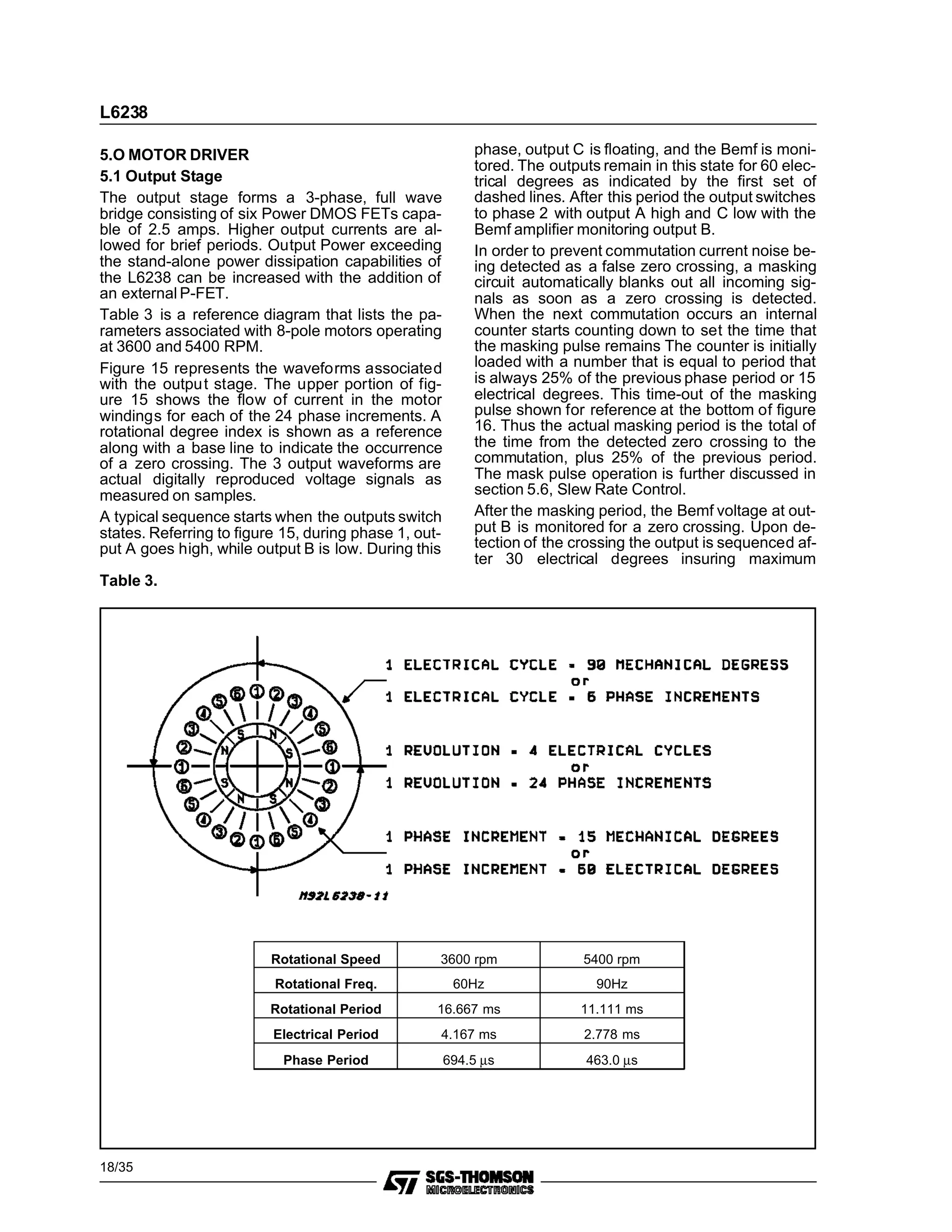
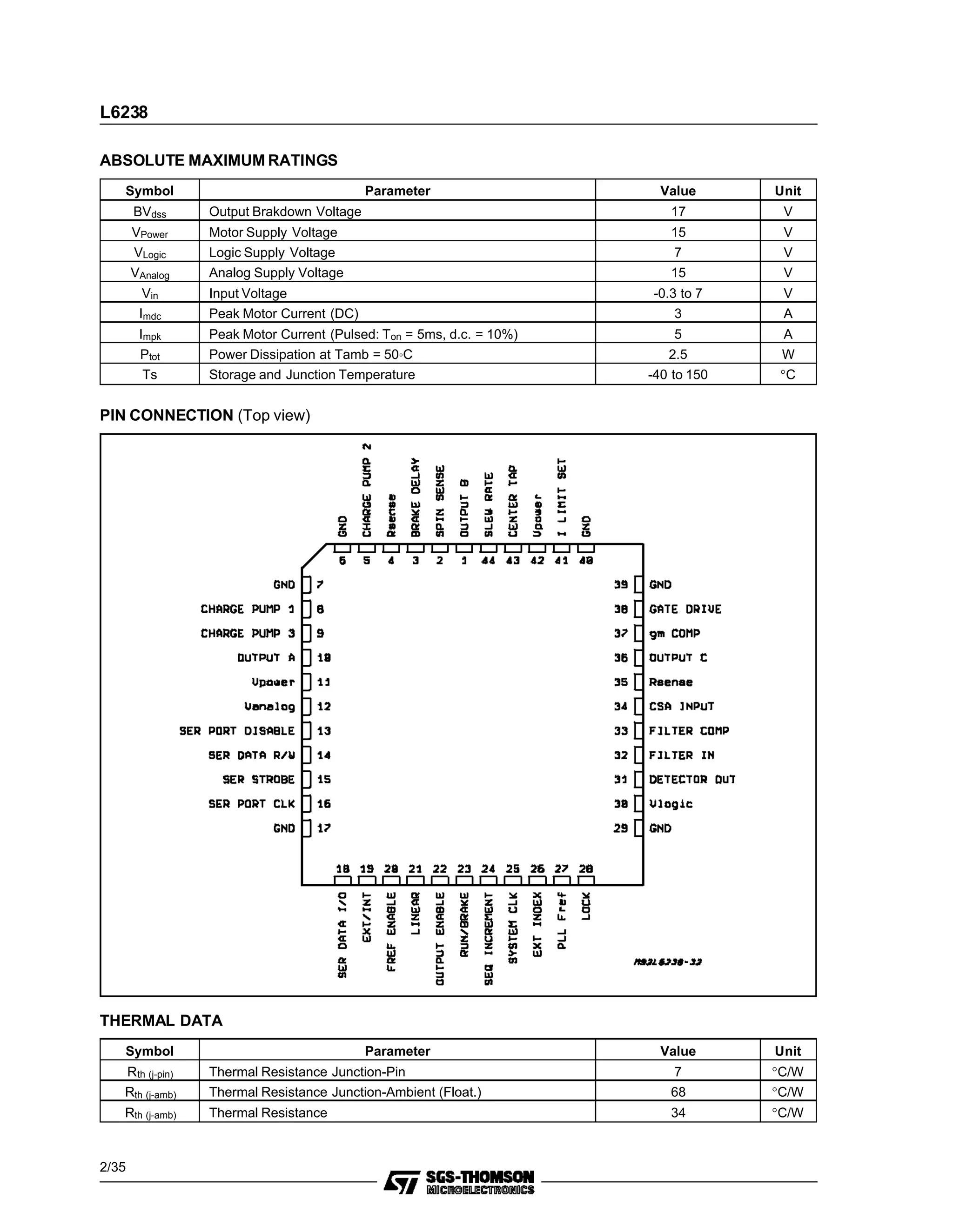
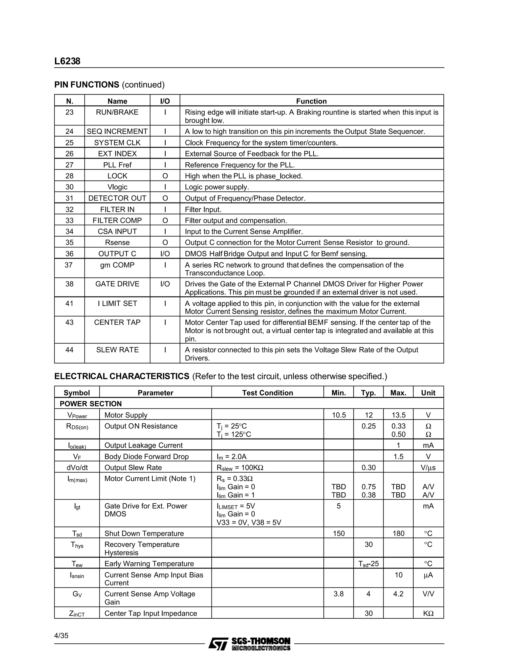
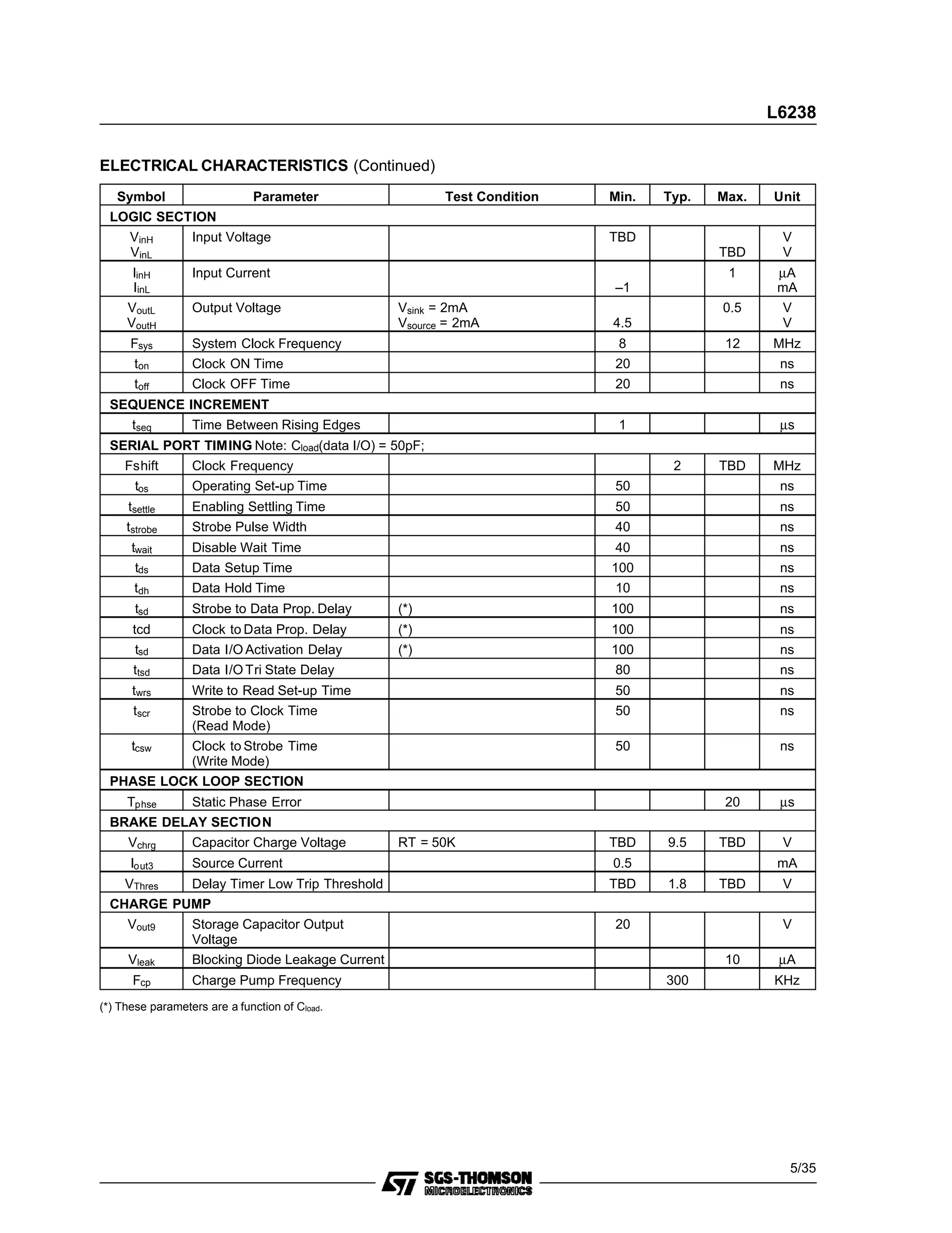
L6238
SENSORLESS SPINDLE MOTOR CONTROLLER
PRODUCT PREVIEW
2.5A, THREE-PHASE OUTPUT DRIVE
PRECISION DIGITAL PLL
FULLY-INTEGRATED ALIGN + GO
START-UP ALGORITHM
DIGITAL BEMF PROCESSING
MASTER/SLAVE SYNCHRONIZATION
BIDIRECTIONAL SERIAL PORT
STAND ALONE OR EXT. DRIVER
SHOOT-THROUGH PROTECTION
DESCRIPTION
The L6238 is a complete Three-Phase, D.C.
Brushless Spindle Motor Driver system. The de-
vice features both the Power and Control Sec-
tions and will operate Stand Alone, or can be
used in Higher Power Applications with the addi-
tion of an external Linear Driver.
Start-Up can be achieved with the Fully-Inte-
grated Align + GO Algorithm or may be se-
quenced manually for User-Defined start-up algo-
rithms.
A Digital PLL provides high accuracy and the ca-
pability to do Master/Slave Synchronization for
Disk Array configurations.
Programmable functions include commutation
Timing Adjustment and Slew Rate Control for
peak efficiency and minimum noise.
Protective features include Stuck RotorBackward
Rotation Detection and Automatic Thermal Shut-
down.
This is advanced information on a new product now in development or undergoing evaluation. Details are subject to change without notice.
June 1993
BLOCK DIAGRAM
PLCC44
ORDERING NUMBER: L6238
1/35
ABSOLUTE MAXIMUM RATINGS
Symbol Parameter Value Unit
BVdss Output Brakdown Voltage 17 V
VPower Motor Supply Voltage 15 V
VLogic Logic Supply Voltage 7 V
VAnalog Analog Supply Voltage 15 V
Vin Input Voltage -0.3 to 7 V
Imdc Peak Motor Current (DC) 3 A
Impk Peak Motor Current (Pulsed: Ton = 5ms, d.c. = 10%) 5 A
Ptot Power Dissipation at Tamb = 50°C 2.5 W
Ts Storage and Junction Temperature -40 to 150 °C
THERMAL DATA
Symbol Parameter Value Unit
Rth (j-pin) Thermal Resistance Junction-Pin 7 °C/W
Rth (j-amb) Thermal Resistance Junction-Ambient (Float.) 68 °C/W
Rth (j-amb) Thermal Resistance 34 °C/W
PIN CONNECTION (Top view)
L6238
2/35
GENERAL DESCRIPTION
The L6238 is an integrated circuit that will be
used to commutate and speed control a 3-Phase,
8-pole, brushless, DC motor. The primary applica-
tion is for disk drive spindle motors. This I.C. has
the following features:
No Motor Hall Effect Sensors are required for
commutation or speed control. Timing informa-
tion is determined from the Bemf voltage of the
undriven motor terminal.
On-board Speed Control via a Phase Locked
Loop that accepts a once-per-rev reference
frequency and locks the motor to that fre-
quency. The L6238 can accomodate a wide
range of speeds.
The L6238 achieves Spindle Synchronization
by locking to a once-per-rev reference that is
common to multiple drives. The L6238 has a
multiplexer that enhances the versatility of the
controller. This first multiplexer selects either
internal feedback, (generated by the Bemf of
the motor), or external feedback (embedded
index).
An External P-Channel FET can be connected
to the FET can be connected to the FET
Bridge for Higher Power Applications.
In this configuration, the internal DMOS drivers
are sequenced in full conduction state and the
external PFET is the linear control element. An
internal inverting buffer from the output of the
OTA controls the conduction of the EXT PFET.
An internal Virtual Center Tap is used if the
motor center tap is not connected.
The motor Current Limit can be set by an ex-
ternal resistor divider.
A Serial Port is included so that I/O can be
done with a minimum of pins. Key control and
status lines are also bonded out to achieve a
Minimum Configuration without using the Serial
Port.
Programmable Functions include Phase
Switch Timing Optimization for motor effi-
ciency, Speed Lock Threshold, Auto-Start or
mP Supervised Spinup, and output current lim-
iting gain.
Energy Recovery Mode for Head Retraction,
followed by Dynamic Braking Mode.
Logic signals are CMOS Compatible.
Stuck Rotor and Backward Rotation detection.
Automatic Thermal Shutdown with early warn-
ing bit available in the status register
PIN FUNCTIONS
N. Name I/O Function
1 OUTPUT B I/O DMOS Half Bridge Output and Input B for Bemf sensing.
2 SPIN SENSE O Toggless at each Zero Crossing of the Bemf.
3 BRAKE DELAY I Energy Recovery time constant, defined by external R-C to ground.
4 Rsense O Outputs A+B connections for the Motor Current Sense Resistor to ground
5 CHARGE PUMP 2 I Negative Terminal of Pump Capacitor.
6, 7,
17, 29,
39, 40
GROUND I Ground terminals.
8 CHARGE PUMP 1 I Positive terminal of Pump Capacitor.
9 CHARGE PUMP 3 I Positive terminal of Storage Capacitor.
10 OUTPUT A I/O DMOS Half Bridge Output and Input A for Bemf sensing.
11, 42 Vpower I Supplies the voltage for the Power Section.
12 Vanalog I 12V supply.
13 SER PORT
DISABLE
I Input for tri-stating the serial port.
14 SER DATA R/W I Selects Serial Data Read or Write Function.
15 SER STROBE I Dtat Strobe Input.
16 SER PORT CLK I Clock for Serial Data Control.
18 SER DATA I/O I/O Data stream Input/Output for Control/Status Registers.
19 EXT/INT I Selects thr Internal BEMF Zero Crossing or an External Source as Feedback
Frequency for te PLL.
20 FREF ENABLE I A zero on this pin passes the PLL Fref signal to the Freq/phase detector.
21 LINEAR I This input should be grounded or left unconnected.
22 OUTPUT
ENABLE
I Tristates Power Output Stage when a logic zero.
L6238
3/35
ELECTRICAL CHARACTERISTICS (Refer to the test circuit, unless otherwise specified.)
Symbol Parameter Test Condition Min. Typ. Max. Unit
POWER SECTION
VPower Motor Supply 10.5 12 13.5 V
RDS(on) Output ON Resistance Tj = 25°C
Tj = 125°C
0.25 0.33
0.50
Ω
Ω
Io(leak) Output Leakage Current 1 mA
VF Body Diode Forward Drop Im = 2.0A 1.5 V
dVo/dt Output Slew Rate Rslew = 100KΩ 0.30 V/µs
Im(max) Motor Current Limit (Note 1) Rs = 0.33Ω
Ilim Gain = 0
Ilim Gain = 1
TBD
TBD
0.75
0.38
TBD
TBD
A/V
A/V
Igt Gate Drive for Ext. Power
DMOS
ILIMSET = 5V
Ilim Gain = 0
V33 = 0V, V38 = 5V
5 mA
Tsd Shut Down Temperature 150 180 °C
Thys Recovery Temperature
Hysteresis
30 °C
Tew Early Warning Temperature Tsd-25 °C
Isnsin Current Sense Amp Input Bias
Current
10 µA
GV Current Sense Amp Voltage
Gain
3.8 4 4.2 V/V
ZinCT Center Tap Input Impedance 30 KΩ
PIN FUNCTIONS (continued)
N. Name I/O Function
23 RUN/BRAKE I Rising edge will initiate start-up. A Braking rountine is started when this input is
brought low.
24 SEQ INCREMENT I A low to high transition on this pin increments the Output State Sequencer.
25 SYSTEM CLK I Clock Frequency for the system timer/counters.
26 EXT INDEX I External Source of Feedback for the PLL.
27 PLL Fref I Reference Frequency for the PLL.
28 LOCK O High when the PLL is phase_locked.
30 Vlogic I Logic power supply.
31 DETECTOR OUT O Output of Frequency/Phase Detector.
32 FILTER IN I Filter Input.
33 FILTER COMP O Filter output and compensation.
34 CSA INPUT I Input to the Current Sense Amplifier.
35 Rsense O Output C connection for the Motor Current Sense Resistor to ground.
36 OUTPUT C I/O DMOS Half Bridge Output and Input C for Bemf sensing.
37 gm COMP I A series RC network to ground that defines the compensation of the
Transconductance Loop.
38 GATE DRIVE I/O Drives the Gate of the External P Channel DMOS Driver for Higher Power
Applications. This pin must be grounded if an external driver is not used.
41 I LIMIT SET I A voltage applied to this pin, in conjunction with the value for the external
Motor Current Sensing resistor, defines the maximum Motor Current.
43 CENTER TAP I Motor Center Tap used for differential BEMF sensing. If the center tap of the
Motor is not brought out, a virtual center tap is integrated and available at this
pin.
44 SLEW RATE I A resistor connected to this pin sets the Voltage Slew Rate of the Output
Drivers.
L6238
4/35
ELECTRICAL CHARACTERISTICS (Continued)
Symbol Parameter Test Condition Min. Typ. Max. Unit
LOGIC SECTION
VinH
VinL
Input Voltage TBD
TBD
V
V
IinH
IinL
Input Current
–1
1 µA
mA
VoutL
VoutH
Output Voltage Vsink = 2mA
Vsource = 2mA 4.5
0.5 V
V
Fsys System Clock Frequency 8 12 MHz
ton Clock ON Time 20 ns
toff Clock OFF Time 20 ns
SEQUENCE INCREMENT
tseq Time Between Rising Edges 1 µs
SERIAL PORT TIMING Note: Cload(data I/O) = 50pF;
Fshift Clock Frequency 2 TBD MHz
tos Operating Set-up Time 50 ns
tsettle Enabling Settling Time 50 ns
tstrobe Strobe Pulse Width 40 ns
twait Disable Wait Time 40 ns
tds Data Setup Time 100 ns
tdh Data Hold Time 10 ns
tsd Strobe to Data Prop. Delay (*) 100 ns
tcd Clock to Data Prop. Delay (*) 100 ns
tsd Data I/O Activation Delay (*) 100 ns
ttsd Data I/O Tri State Delay 80 ns
twrs Write to Read Set-up Time 50 ns
tscr Strobe to Clock Time
(Read Mode)
50 ns
tcsw Clock to Strobe Time
(Write Mode)
50 ns
PHASE LOCK LOOP SECTION
Tphse Static Phase Error 20 µs
BRAKE DELAY SECTION
Vchrg Capacitor Charge Voltage RT = 50K TBD 9.5 TBD V
Iout3 Source Current 0.5 mA
VThres Delay Timer Low Trip Threshold TBD 1.8 TBD V
CHARGE PUMP
Vout9 Storage Capacitor Output
Voltage
20 V
Vleak Blocking Diode Leakage Current 10 µA
Fcp Charge Pump Frequency 300 KHz
(*) These parameters are a function of Cload.
L6238
5/35
FUNCTIONAL DESCRIPTION
1.0 INTRODUCTION
1.1 Typical Application
In a typical application, the L6238 will operate in
conjunction with the L6243 Voice Coil Driver as
shown in Fig. 1. This configuration requires a
minimum amount of external components while
providing complete stand-alone operation.
Figure 1: Stand Alone Configuration
L6238
6/35
1.2 Input Default States
Figure 2 depicts the two possible input structures
for the logic inputs. If a particular pin is not used
in an application, it may either be connected to
ground or VLOGIC as required, or simply left un-
connected. If no connection is made, the pin is
either pulled high or low by internal constant cur-
rent generatorsas shown
A listing of the logic inputs is shown with the cor-
respondingdefault state.
1.3 Naming Convention
In order to differentiate between the various types
of control and status signals, the following naming
convention is used.
BOLD CAPITALS - Device pins.
Italics - Serial port control and status signals.
Three input signals form a special case. Referring
to figure 3, the RUN/BRAKE input pin and the
Run/Brake control signal form a logical AND func-
tion, while OUTPUT ENABLE and Output Enable
form an OR function. The outputs signal names,
in Bold Lower case labeled Run/Brake and Out-
put Enable will be used when referring to these
signals. Although not shown, SEQUENCE IN-
CREMENT and Sequence Increment also form
an OR function, with the resultant output signal
called Sequence Increment.
1.4 Modes of Operation
There are 5 basic modes of operation.
1) Tristate
When Output Enable is low, the output power
drivers are tristated.
2) Start-Up
With Output Enable high, bringing Run/Brake
from a low to a high will energize the motor and
the system will be driven by the Fully-Integrated
StartUp Algorithm. A user-defined Start-Up Algo-
rithm, under control of a MicroProcessor, can be
achieved via a serial port and/or external control
pins.
3) Run
Identified by the Lock signal, Run mode is
achieved when the motor speed (controlled by the
Internal PLL) reaches the nominal speed within a
predefined phase error.
4) Park
When Run/Brake is brought low, energy to park
the heads may be derived from the rectified Bemf.
The energy recovery time is a function of the
Brake Delay Time Constant. In this state, the qui-
escent current of the device is minimized (sleep
mode).
5) Brake
After the Energy Recovery Time-Out, the device
is in Brake, with all lower Drivers in full conduc-
tion.
During a power down, the Park Mode is triggered,
followed by a Dynamic Brake.
There are two mutually exclusive conditions
which may be present during the Tristate Mode
(wake up):
Figure 2: InputStructures
FUNCTION CONFIGURATION
PORT DIS
STROBE
PORT CLK
R/W
DATA I/O
EXT/INT
FREF ENABLE
LIN
OUTPUT ENABLE
RUN/BRAKE
SEQ INCR
SYS CLOCK
EXT INDEX
PLL FREF
PULL-UP
PULL-DOWN
PULL-UP
PULL-UP
PULL-UP
PULL-DOWN
PULL-DOWN
PULL-DOWN
PULL-DOWN
PULL-UP
PULL-DOWN
PULL-UP
PULL-UP
PULL-UP
Figure 3: Input Logic
L6238
7/35
a)the spindle is stopped.
b)the system is still running at a speed that
allows for resynchronization.
In order to minimize the ramp up time, the micro-
controller has the possibility to:
check the SPIN SENSE pin, (which toggles at
the Bemf zero crossing frequency)
enable the power to the motor based on the
previous information. Otherwise the uP may is-
sue a Brake command, followed by the start-
up procedure after the motor has stopped spin-
ning.
Brake
W/Mask
Hold & wait
for decision
Tri-state
W/Mask
Tri-state
W/Mask
RunBrk = 1
OutEna = 0
RunBrk = 1
OutEna = 1
OutEna = 1
&
RunBrk = 0
Run
W/Mask
Hold for
”Align & Go”
RunBrk
=
0
OutEna
=
0
Power
on
Reset
OutEna
=
1
RunBrk
=
1
RunBrk
=
0
RunBrk = 0
OutEna = 0
SeqInc = X
R
u
n
B
r
a
k
e
=
1
R
u
n
B
r
a
k
e
=
0
Run
Wo/Mask
SeqInc = 0
SeqInc = 1
SeqInc = 0
SeqInc = 1
Action across
line increments
sequencer
Auto Start-up
Enabled Disabled
RunBrk = 1
OutEna = 0
RunBrk = 1
OutEna = 1
O
u
t
E
n
a
=
0
O
u
t
E
n
a
=
1
Hold for
”Align & Go”
Start
”Align & Go”
Align =
Seqncr.
[Align
to
Phase
#
1]
StkRtr
=
0
[Align
to
Phase
#
3]
O
u
t
E
n
a
=
0
O
u
t
E
n
a
=
0
O
u
t
E
n
a
=
0
Align =
0
G
o =
0
Align
=
1
RunBrk
=
1
From Anywhere
Hold
for
”Resync”
Start
”Resync”
Resync = 1
Release
min mask
Run
G
o =
1
(Get
1st
Zc)
Zc
Reset
=
RunBrk = 1
OutEna = 0
O
u
t
E
n
a
=
0
O
u
t
E
n
a
=
0
O
u
t
E
n
a
=
0
No Zc
No Zc
Auto/Ext = 0
Stuck
Rotor
(hold)
(G
et 2
nd Z
c)
Zc R
eset=
OutEna = 1
&
RunBrk = 1
StrRtr = 0
StrRtr = 0
Mono
=
0
RunBrk = 0
&
OutEna = 0
Figure 4: State Diagram
L6238
8/35
2.0 STATE DIAGRAMS
2.1 State Diagram
Figure 4 is a complete State Diagram of the con-
troller depicting the operational flow as a function
of the control pins and motor status. The flow can
be separatedinto four distinct operations.
2.2 Align + Go
Figure 5 represent the normal flow that will
achieve a spin-up and phase lock of the spindle
motor. Upon power up, the controller first checks
to determine if the motor is still spinning. This
”Hold For Resync” decision block will be dis-
cussed later.
Hold & wait
for decision
RunBrk = 0
RunBrk = 1
Hold for
”Align & Go”
Hold
for
”Resync”
Start
”Align & Go”
Align =
Seqncr.
Run
[Align
to
Phase
#
1]
Go
=
1
[Align
to
Phase
#
3]
O
u
t
E
n
a
=
0
O
u
t
E
n
a
=
0
O
u
t
E
n
a
=
0
Align =
0
Go =
0
Power
on
Reset
Align
=
1
RunBrk
=
1
OutEna
=
1
OutEna
=
0
RunBrk = 1
OutEna = 0
OutEna = 0
&
RunBrk = 0
Figure 5: Align+Go
L6238
9/35
Assuming the motor is stationary, with Output
Enable high and Run/Brake low, the controller is
in the ”Hold for Align & GO” state. When
Run/Brake is brought high, the motor is in align
mode with Phase 1 active (Output A high and
Output B low). Align is a zero. After the align
time-out (user-programmable), the Align bit goes
high and the sequencer double increments the
outputs to Phase 3 (Output B high and Output C
low). After the next time-out, the controller enters
the Go mode, with the sequencer automatically
incrementing the output phase upon detection of
the motor’s Bemf.
Never command an Align & Go unless a refer-
ence signal is present at PLL FREF, since this
is the signal that determines the length of time
that phase 1 remains active.
If Run/Brake is brought low, (or if the 5V supply
is removed) the controller will revert to ”Hold for
Align & GO” and the serial port will be reinitial-
ized. In order to prevent an erroneous restart con-
dition, it is necessary that Run/Brake be held low
until the motor has completely stopped. Once the
motor has stopped, Run/Brake may be brought
high for a complete Align & Go Start-Up routine.
2.3 Resynchronization
If power is momentarily lost, the sequencer can
automatically resynchronize to the monitored
Bemf. This resychronization can either occur
whenever Output Enable is first brought low then
high or if the Logic Supply is momentarilylost.
Referring to figure 6, the ”Hold for Resync” state
is entered upon POR (Power On Reset) or when-
ever Output Enable is brought low. The control-
ler leaves this state and enters ”Start Resync”
when Output Enable is high.
If zero crossings are detected, the sequencer will
automatically lock on to the proper phase and
bring the motor speed up to Phase Lock.
This resynchronization will take effect with the
motor speed running as low as typically 30% of
it’s nominal value.
Never command an Align & Go while the mo-
tor is spinning. Always initiate a resync first
or initiate brake mode and allow the motor to
spin down.
Power
on
Reset
Hold
for
”Resync”
Start
”Resync”
Resync=1
Release
min mask
Run
OutEna=1
(Get
2nd
Zc)
Zc
Reset
=
(Get
1st
Zc)
Zc
Reset
=
RunBrk=1
OutEna=0
O
u
t
E
n
a
=
0
O
u
t
E
n
a
=
0
O
u
t
E
n
a
=
0
No Zc
No Zc
Figure 6: Resync.
L6238
10/35
2.4 Stuck Rotor/Monotonicity
Refer to figure 7. In order to alert the microproc-
essor of fault conditions, two bits are available in
the Serial Port’s Status Register.
1. Stuck Rotor
If the controller enters the Go mode after the Dou-
ble Align, Bemf must be detected within 419ms
when using a system clock frequency of 10MHz.
If this condition is not met, the outputs will be tris-
tated and set this bit to a zero. The controller en-
ters the ”Stuck Rotor Hold” state.
2. Mono
When the motor spins up normally, the resultant
S P IN SENSE pulses rise in frequency in a
monotonic pattern. Any fault condition that would
cause a rapid decrease in the SPIN SENSE fre-
quency would be detected by internal counters
setting the MONO bit low and forcing a Brake
condition
2.5 External Sequencing
Although the user-defined Start-Up Algorithm is
flexible and will consistently spin up a motor with
minimum external interaction, the possibility ex-
ists where certain applications might require com-
plete microprocessor control of start-up.
The L6238 offers this capability via the SE-
QUENCE INCREMENT input. Referring to figure
9, with Output Enable and Run/Brake low, the
controller is in the ”Hold and Wait for Decision”
state. If the SEQUENCE INCREMENT pin is
brought high during this state, the Auto StartUp
Algorithm is disabled and the sequencer can be
controlled externally.
When Output Enable and Run/Brake are
brought high, the sequencer is incremented every
time that the SEQUENCER INCREMENT pin is
first brought low and then high. During the time
that this pin is high, all Bemf information is
R un
S tu c k
Ro t or
(h ol d)
O ut En a = 1
&
Ru nB rk = 1
Mono
=
0
StkRtr
=
0
Figure 7: Stuck Rotor/Monotonicity.
Brake
W/Mask
Hold & wait
for decision
Tri-state
W/Mask
Tri-state
W/Mask
RunBrk = 1
OutEna = 0
RunBrk = 1
OutEna = 1
OutEna = 1
&
RunBrk = 0
Run
W/Mask
Hold for
”Align & Go”
RunBrk
=
0
OutEna
=
0
Power
on
Reset
OutEna
=
1
RunBrk
=
1
RunBrk
=
0
RunBrk = 0
OutEna = 0
SeqInc = X
Hold
for
”Resync”
R
u
n
B
r
a
k
e
=
1
R
u
n
B
r
a
k
e
=
0
RunBrk = 1
OutEna = 0
Run
Wo/Mask
SeqInc = 0
SeqInc = 1
SeqInc = 0
SeqInc = 1
Action across
line increments
sequencer
Auto Start-up
Enabled Disabled
RunBrk = 1
OutEna = 0
RunBrk = 1
OutEna = 1
O
u
t
E
n
a
=
0
O
u
t
E
n
a
=
1
OutEna = 0
&
RunBrk = 0
Figure 8: Ext. Sequence.
L6238
11/35
masked out, and when it is low, the Bemf informa-
tion can be detected normally. When the motor
has reached a predetermined speed, the SE-
QUENCE INCREMENT pin can be left low and
the L6238 Motor Control logic will take over and
automaticallybring the motor into Phase Lock.
3,0 START-UP ALGORITHMS
3.1 Spin-Up Operation
The spin operation can be separated into 3 parts:
1) Open Loop Start-Up - The object is to create
motion in the desired direction so that the Bemf
voltages at the 3 motor terminals can provide reli-
able information enabling a transition to closed
loop operation.
2) Closed Loop Start-Up - The Bemf voltage
zerocrossings provide timing information so that
the motor can be accelerated to steady state
speed.
3) Steady-State Operation - The Bemf voltage
zero-crossings provide timing information for pre-
cision speed control.
The L6238 contains features that offer flexible
control over the start-up procedure. Either the on-
board Auto-Start Algorithm can be used to control
the start-up sequence or more sophisticated exte-
mal start-up algorithms can be developed using
the Serial Port and key control/sense functions
brought out to pins.
3.2 Auto-Start Algorithm
The Serial Port Control Bit Auto/Ext (Refer to Ta-
ble 2), controls the start-up mode. The power up
default state is a logic high which selects the
AutoStart Mode. When Run/Brake is low, the
L6238 is in brake mode, and the Auto-Start Algo-
rithm is reset. In the brake mode, all of the lower
DMOS drivers are ON, and the upper drivers are
OFF.
Note that Run/Brake should be brought low for a
period exceeding the value selected for the brake
delay time in order to initialize the brake delay cir-
cuit.
The Auto-Start Algorithm is based on an Align &
Go approach and can be visualized by referring to
Figure 9. Shown are the Output Enable and
Run/Brake control signals, sequencer output with
the resultant output phases, and the Align and Go
status bits. The times labeled Tl and T2 are two
Figure 9: Auto Start Profile
Tasd <1> Tasd <0> Ta = T1 T2 Tg
0
0
1
1
0
1
0
1
0.178 s
0.356 s
0.533 s
0.711 s
0.533 s
1.067 s
1.600 s
2.133 s
0.711 s
1.422 s
2.133 s
2.844 s
Note: PLL Reference Frequency = 90Hz
L6238
12/35
delays that are 25% and 7S% respectively of the
total delay selected by the Auto-Start Delay Con-
trol Bits. The times labled T1 and T2 are the times
associated wim the Align and Go status bits. Typi-
cal delays associated with these times for a PLL
reference frequency of 90Hz are shown in the fig-
ure.
Referring to figure 9, the following is the se-
quence of events during Auto-Start:
Alignment Phase
- Output Stage is energized to phase 1 with
OUTPUT A high and OUTPUT B low for T
seconds.
- The intemal sequencer double increments the
output stage to Phase 3 for T2 seconds. If
phases 1 or 3 are high torque states, the mo-
tor should become aligned.
- During the alignment phase, the SEQ INCRE-
MENT signal is ignored.
Go Phase
- The internal sequencer double increments the
output stage to State 5, which should produce
torque in the desired direction.
- with SEQ INCREMENT held low, the se-
quencer is now controlled by the Bemf zero
crossings, and the motor should ramp up to
speed.
If backward rotation is detected, a status bit in the
serial port will be set, and the L6238 will revert to
the brake mode.
- If a stuck rotor condition exists, the Stuck Ro-
tor Status bit is flagged, but no action is
taken. If though during a stuck rotor condition,
the time out due to the backwards rotation oc-
curs, the L6238 will revert back to the brake
mode.
3.3 Externally Controlled Start-Up Algorithms
Enhanced Start-Up Algorithms can be achieved
by using a uProcessorto interact with the L6238’s
control and status signals. The uProcessor needs
to be heavily involved during Open Loop Start-Up.
The L6238 has the ability to transition to Closed
Loop Start-Up at very low speeds, reducing the
uProcessor task to monitoring status rather than
real time interaction. Thus, it is a perfect applica-
tion for an existing uProcessor.
To allow control via an external means, the
Auto/Ext Control Bit in the Serial Port must be set
low. This disables the internal Auto-Start Algo-
rithm. The following control and status signals al-
low for very flexible algorithm development:
SEQ_INCR A low to high transition at this input
is used to increment the state of the power out-
put stage. It is useful during start-up, because
the µProcessor can cycle to any desired state,
or cycle through the states at any desired rate.
When held high, it inhibits the BEMF zero
crossings from incrementing the internal se-
quencer.
SPIN SENSE This output is low until the first
detected Bemf zero crossing occurs. It then
toggles at each successive zero crossing. This
signal serves as a motion detector and gives
useful timing information as well.
LOCK A high denotes that the phase error be-
tween the PLL reference and the feedbacksig-
nals is within the programmed threshold. This
signal is updated once per revolution.
Seq Reset This bit is used to reset the output
stage to the first state.
3.4 Start Up Approaches
Align & Go Approach The Align & Go approach
provides a very time efficient algorithm by ener-
gizing the coils to align the rotor and stator to a
known phase. This approach can be achieved via
the Seq Reset, or by sequencing SEQ INCR.
SPIN SENSE can be monitored to assure that
motion occurred. Once ample time is given for
alignment to occur, SEQ INCR can be double in-
cremented, and the SPIN SENSE pin can be
monitored to detect motion. When SEQ INCR is
pulled low, control is transferred to the internal se-
quencer, and the L6238 finishes the spinup op-
eration. If no motion is detected, SEQ INCR can
be incremented to a different phase and the proc-
ess can be repeated. The alignment phase may
cause backward rotation, which on the average
will be greater than the Stepper Motor approach.
The Auto-Start algorithm described earlier is an
Align & Go approach. The main advantages of
the integrated Auto-Start are that the uP is not in-
volved real-time, and there are a minimum of in-
terface pins required to the spindle control sys-
tem.
Stepper Motor Approach This approach mini-
mizes backward rotation by sequencing SEQ
INCR at an initial rate that the rotor can follow.
Thus, it is driven in a similar fashion to a stepper
motor. The rate is continuallyincreased until the
Bemf voltage is large enough to reliably use the
zero-crossings for commutation timing. SEQ
INCR is held low, causing control to be passed to
the L6238’s internal sequencer as in the Align &
Go approach.
The Stepper Motor approach takes longer than
the Align & Go approach because the initial com-
mutation frequency and subsequent ramp rate
L6238
13/35
must be low enough so that the motor can follow
without slipping. This implies that to have a reli-
able algorithm, the initial frequency and ramp rate
must be chosen for the worst case motor under
worst case conditions.
4.0 DIGITAL PLL MOTOR SPEED CONTROL
4.1 Phase Detector
The internal Phase/Frequency Detector of the
PLL has two inputs:
- reference input (Fref)
- feedback input (Fmtr)
The feedback Input is multiplexed between the in-
ternal Bemf Zero Crossing Detector and an exter-
nally provided sync pulse (EXT INDEX)
Shown in figure 10 is the classical state diagram
for a phase detector along with waveform exam-
ples.
Positive phase is defined as when the reference
falling edge occurs before the falling edge of
Fmotor and the motor speed must be increased.
Negative phase is just the opposite, requiring a
slowing of the motor speed.
As an example, the top four waveforms in figure
10 represent a positive phase condition. In this
case the ”up” signal would go low since the refer-
ence signal went low before the appearance of a
negative transition of fmotor. The falling edge of
fmotor causes the ”up” signal to revert back to a
high. The period while the ”up” signal is in a low
state is a function of the phase difference.
Figure 10: Phase Detector State Diagram.
L6238
14/35
4.2 Counter Section
Figure 11 is a block diagram of the counter sec-
tion of the PLL along with the phase detector.
The phase detector provides up and down signals
that are used to control the direction and counting
period of two 8 bit counters. Two counters are
used to provide both coarse and fine phase error
information. The coarse counter operates to bring
the phase error into a finite window, while the fine
counter with it’s higher resolution controls the
phase jitter to typically 5µs.
As an example, during a positive phase measure-
ment, the counters are reset to 10000000 which
is the middle of their measurement range corre-
sponding to zero degrees phase error. The falling
edge of Fref, in conjunction with the ”up” signal,
causes the fine counter to then start counting up.
The coarse counter is inhibited by the fine counter
until the fine counter has reached it’s maximum
count. The falling edge of Fmtr causes the count-
ers to stop counting and the bits in the fine and
course counters are then latched into their re-
spective latches. The counters are then reset to
10000000 in anticipation of the next phase meas-
urement.
The operation of the counter section during spin-
up and phase lock can be described in three
phases:
1) Initial Spin-Up - At start-up the PLL will inher-
ently bring the motor speed ”in line” with the refer-
ence frequency.The phase detector is initialized
at power up to force the countersto start counting
up.
Since there will be many more Fref. vs Fmtr fall-
ing edges at start-up, the width of the ”up” pulse
will be wide. The fine counter will reach it’s maxi-
mum count and send an enable pulse to the
coarse counter causing it to start counting. After
127 counts, the coarse counter also reaches it’s
maximum count. At the end of the ”up” pulse, it’s
rising edge loads the outputs of the Coarse and
Fine counters into corresponding latches. Thus
the latches are updated once-per-rev with a bi-
nary number that corresponds to the measured
phase error. This count will be converted via a
Digital to Analog Convertors (DAC) into a speed
Command Voltage, which at start-up will be the
maximum as set by the ILIM SET voltage.
2) Overshoot - As the motor speed increases
close to the reference, the coarse counter comes
out of compliance and decreases it’s count as the
phase difference becomes smaller. The fine
counter then takes over when the phase is in a
certain range. A certain amount of phase over-
shoot will take place as the motor passes though
zero phase difference due to the closed loop sys-
tem response characteristics.
This will cause the counters to count down to
”slow” the motor down until the phase difference
is minimal.
Figure 11: Logic Block Diagram.
L6238
15/35
3) Phase Lock - After a brief settling time, typi-
cally 1-2 seconds after spin-up, the counters will
alternately count up and down as required to
maintain the phase difference to be as close to
minimum as possible. The counter outputs at this
time should be ”hovering” around 10000000.
The outputs of the two DACs are sent to latches
that store the digital representation of the meas-
ured phase error. This information is then bussed
to the DACs.
4.3 Coarse/Fine DACs
Two DACs are used to convert the digital phase
error information into an analog voltage that can
be used to command the output driver’s current.
In figure 12, the two 8-bit digital error signals are
used to switch in 256 possible voltages derived
from a precision Band-Gap reference. The same
resistor ladder string is used for the Coarse and
Fine DACs. The outputs of the DACS are then
sent to buffer stages and added together via a
summing amplifier.
4.4 Transfer Functions
Figure 13 represent the Output Voltage vs Phase
Error for the Coarse and Fine DACs depicting the
resolution that is achievable.
Table 2 shows examples of the resolution of both
Figure 12: Coarse and Fine DAC’s.
Table 2
Fsystem
Clock
Fcoarse
Phase LSB
Coarse
(Range)
Coarse
Ffine
Phase LSB
Fine
(Range)
Fine
8MHz 15.6KHz 64.1µs 16.3ms 1.0MHz 1.0µs 255µs
10MHz 19.5KHz 51.3µs 13.1ms 1.25MHz 800ns 204µs
12MHz 23.4KHz 42.7µs 10.9ms 1.5MHz 667ns 170µs
L6238
16/35
DACs as a function of the system clock repetition
rate. Fcoarse is the system clock divided by 512,
while Ffine divides the clock by 8. This gives for
example, Coarse and Fine LSB’s of 51.3us and
800ns respectively for a system clock repetition
rate of 10MHz. Therefore the best phase jitter that
could be achieved as a function of the counter
resolution is 800ns. The dynamic range of each
counter is also shown in the table.
It can be seen that the ratio of Fine to Coarse
counts is 64. The summing amplifler divides the
Fine DAC buffer output voltage by a factor of 16.
Therefore there is a 4:1 ratio of Fine to Coarse
gain.
This results in a Speed Control Loop that is fairly
easy to compensate with excellent transient re-
sponse.
The output of the PLL Detector is fed to a gener-
al purpose. filter amplifier that is used to compen-
sate the Speed Control Loop. The filter amplifier
output stage has been carefully designed to limit
the compliance voltage to a value that tracks the
Ilim Set voltage, thus limiting the amount of over-
shoot and enhancing the transient response of
the loop.
4.5 PLL Detector Output
Figure 14 is a graph of the typical DETECTOR
OUTPUT voltage as a function of the detected
phase difference as measured on production ma-
terial. The change of the gain slope is apparent
around the zero phase difference point. With the
spindle motor at phase lock, the DETECTOR
OUTPUT voltage is typically 2.0, equivalent to the
internal Virtual Ground level.
Figure 13: Coarse/Fine DAC’s Output Graphs.
Figure 14: Vdetector Output vs Phase Error.
L6238
17/35
5.O MOTOR DRIVER
5.1 Output Stage
The output stage forms a 3-phase, full wave
bridge consisting of six Power DMOS FETs capa-
ble of 2.5 amps. Higher output currents are al-
lowed for brief periods. Output Power exceeding
the stand-alone power dissipation capabilities of
the L6238 can be increased with the addition of
an external P-FET.
Table 3 is a reference diagram that lists the pa-
rameters associated with 8-pole motors operating
at 3600 and 5400 RPM.
Figure 15 represents the waveforms associated
with the output stage. The upper portion of fig-
ure 15 shows the flow of current in the motor
windings for each of the 24 phase increments. A
rotational degree index is shown as a reference
along with a base line to indicate the occurrence
of a zero crossing. The 3 output waveforms are
actual digitally reproduced voltage signals as
measured on samples.
A typical sequence starts when the outputs switch
states. Referring to figure 15, during phase 1, out-
put A goes high, while output B is low. During this
phase, output C is floating, and the Bemf is moni-
tored. The outputs remain in this state for 60 elec-
trical degrees as indicated by the first set of
dashed lines. After this period the output switches
to phase 2 with output A high and C low with the
Bemf amplifier monitoring output B.
In order to prevent commutation current noise be-
ing detected as a false zero crossing, a masking
circuit automatically blanks out all incoming sig-
nals as soon as a zero crossing is detected.
When the next commutation occurs an internal
counter starts counting down to set the time that
the masking pulse remains The counter is initially
loaded with a number that is equal to period that
is always 25% of the previous phase period or 15
electrical degrees. This time-out of the masking
pulse shown for reference at the bottom of figure
16. Thus the actual masking period is the total of
the time from the detected zero crossing to the
commutation, plus 25% of the previous period.
The mask pulse operation is further discussed in
section 5.6, Slew Rate Control.
After the masking period, the Bemf voltage at out-
put B is monitored for a zero crossing. Upon de-
tection of the crossing the output is sequenced af-
ter 30 electrical degrees insuring maximum
Table 3.
Rotational Speed 3600 rpm 5400 rpm
Rotational Freq. 60Hz 90Hz
Rotational Period 16.667 ms 11.111 ms
Electrical Period 4.167 ms 2.778 ms
Phase Period 694.5 µs 463.0 µs
L6238
18/35
Figure 15: Brake Delay.
L6238
19/35
torque. The spin sense waveform at the bottom of
the figure indicates that this output signal toggles
with each zero crossing.
5.2 Brake Delay
When Run/Brake is brought low, a brake is initi-
ated. Referring to figure 16, SWI is opened and
the brake delay capacitor, Cbrake, is allowed to
discharge towards ground via Rbrake. At the same
time, switches SW2 through SW7 bring the gates
of the output FETs to ground halting conduction,
causing the motor to coast. While the motor is
coasting, the Bemf is used to park the heads.
When Cbrake reaches a voltage that is below the
turn ON threshold of Q I, Switches SW8, 9 and 10
bring the gates of the lower drivers to Vbrake po-
tential. This enables the lower FETs causing a
braking action. This braking action also occurs if
the logic supply is lost. The analog supply is not
monitored in the L6238 since the L6243 already
monitors this voltage and initiates a Park function
when this supply drops to a predetermined level.
If multiple logic supplies are used in the applica-
tion, all logic signals to the L6238 including the
reference and clock signals should be buffered
with gates powered by the same supply as the
L6238 in order to prevent erroneous operation.
This would occur, for example, if the 5V supply to
the controller were lost while 5V were still present
at one of the logic pins. This would partially power
the chip, causing unpredictable operation.
5.3 Charge Pump
The charge pump circuitry is used as a means of
doubling the analog supply voltage in order to al-
low the upper N-channel DMOS transistors to be
driven like P-channel devices. The energy stored
in the reservoir capacitor is also used to drive the
Figure 16: Brake Delay.
L6238
20/35
lower drivers in a brake mode if the analog supply
is lost.
Figure 17 is a simplified schematic of the charge
pump circuitry. A capacitor, Cpump, is used to re-
trieve energy from the analog supply and then
”pumps” it into the storage capacitor, Cresvr. An in-
ternal 300kHz oscillator first turns ON Q2 to
quickly charge Cpump to approximately the rail
voltage. The oscillator then turns ON Ql while
turning OFF Q2. Since the bottom plate of Cpump
is now effectively at the rail potential, Cresvr is
charged to ~ twice the rail voltage via D2. A zener
referenced series-pass regulator supplies a volt-
age, Vbrake, during brake mode.
5.4 Output Current Control
The output current is controlled in a linear fashion
via a transconductance loop. Referring to figure
18, the sourcing FET of one phase is forced into
full conduction by connecting the gate to Vpump,
while the sinking transistor of an appropriate
phase operates as a transconductance element.
To understand the current control loop, it will be
assumed that Q2 in figure 18 is enabled via SW2
by the sequencer.
During a run condition, the current in Q2 is moni-
tored by a resistor R4 connected to the Rsense in-
put. The resulting voltage that appears across R4
is amplified by a factor of four by A3 and is sent to
A2 where it is compared to the PLL error signal.
A2 provides sufficient drive to Q2 in order to
maintain the motor speed at the proper level as
commanded by the PLL.
During initial start-up, the error signal from the
output of the PLL Phase/Frequency Detector will
be at compliance in order to quickly bring the mo-
tor up to correct speed. The motor current during
this condition can be safely limited to a predeter-
mined value by applying a voltage to the ILIM
SET input.
The voltage at this input is buffered by A1 and
sent to multiplexer, SWl. The output voltage of the
multiplexer, Vclmp, is used to control the maxi-
mum non-inverting input voltage for amplifier A2.
This multiplexer also receives a voltage that is 1/2
the ILIM SET value via a resistor divider con-
nected to the buffer. Control bit llim Gain deter-
mines which voltage is available at the output of
the multiplexer and allows a 2:1 change in the
output current limit under software control.
For example, if the Ilim Gain control bit is set
high, and 3.3V were applied to the ILIM SET in-
put, then Vclmp would equal 1.65V. Since A3 has
a voltage gain of 4, this would translate to a maxi-
mum sensed voltage at the Rsense input equal to
0.41V. If Rslew were selected to be 0.33 Ω, then
the maximum output current would be limited to
~1.25A.
By setting the Ilim Gain control bit low, Vclmp now
equals ILIM SET, and the clamped sensed volt-
age at the Rsense input would be doubled to
0.82V, allowing a maximum of 2.5A at the output.
Figure 17: Charge Pump Circuit.
L6238
21/35
5.5 Transconductance Loop Stability
The RC network connected to the Compensation
pin provides for a single pole/zero compensation
scheme. The pole/zero locations are adjusted
such that a few dB of gain (typ. 20dB) remains in
the transconductance loop at frequencies higher
than the zero.
The inductive characteristic of the load provides
Figure 18: LinearControl Loop.
Figure 19: Control Loop Response.
L6238
22/35
the pole necessary for loop stability. Thus the
loop bandwidth is actually limited by the motor it-
self.
Figure 19 shows the complete transconductance
loop including compensation, plus the response.
The Bode plot depicts the normal way to achieve
stability in the loop. The pole and zero are used to
set a gain of 20dB at a higher frequency and the
pole of the motor cuts the gain to achieve stabil-
ity.
Loop instability may be caused by two factors:
1)The motor pole is too close to the zero. Refer-
ring to figure 20, the zero is not able to decre-
ment the shift of phase, and when the effect
of the pole is present, the phase shift may
reach 180° and the loop will oscillate. To rec-
tify this situation, the pole/zero must be
shifted at lower frequencies by increasing the
compensationcapacitor.
2)The motor capacitance, CM, itself can inter-
fere with the loop, creating double poles. If
the gain at higher frequenciesis low, this dou-
ble pole will not be able to reach a critical
value due to it’s 40dB/decade slope. Figure
21 illustrates performance with low gain. Al-
though the gain decrease at a rate of
40dB/decade,the phase does not reach 180°
of shift.
If the gain at higher frequencies is sufficiently
high, the double pole slope of 40dB/decade can
cause the phase shift to reach 180°, resulting in
oscillation. Figure 22 is a Bode plot showing how
to correct this situation. The bold line indicates
the response with relatively high gain at the
higher frequencies. By leaving the pole un-
changed and increasing the zero, the response
indicated by the dashed lines can be achieved.
5.6 Slew Rate Control
A 3-phase motor appears as an inductive load to
the power supply. The power supply sees a dis-
turbance when one motor phase turns OFE and
another turns ON because the FET turn-OFF time
is much shorter than the L/R rise time. Abrupt
FET turn-OFF without a proper snubbing circuit
can even cause current recirculation back into the
supply.
However, the need for a snubber circuit can be
eliminated by controlling the turn-OFF time of the
FETs.
Figure 20: Motor Pole.
Figure 21: Effect of Cm.
Figure 22: Correct Compensation.
L6238
23/35
Referring back to figure 18, the rate at which the
upper and lower drivers turn OFF is programma-
ble via an external resistor, Rslew connected to the
SLEW RATE pin. This resistor defines a current
which is utilized internally to limit the voltage slew
rate at the outputs during transition, thus minimiz-
ing the load change that the power supply sees.
Figure 23 is a plot of the slew rate that will be ob-
tained as a function of the resistor connected to
the SLEW RATE pin. The voltage at the this pin
is typically 2.4V.
To insure proper operation the range of resistor
values indicated should not be exceeded and in
some applications values near the end points
should be avoided as discussed below.
Low Values of Rslew - If a relativelylow value of
Rslew is selected, the resultant fast slew rate will
result in increased commutation cross-over cur-
rent, higher EMI, and large amount of commuta-
tion current.
This last case can cause voltage spikes at the
output that can go as much as lV below ground
level. This situation must be avoided in this inte-
grated circuit (as in most) since it causes unpre-
dictable operation.
High Values of Rslew - Higher values of Rslew
result of course in slow slew rates at the outputs
which is, under most conditions, the desired case
since the problems associated with fast rates are
reduced. The additional advantage is lower
acoustical noise.
Problems can occur though if the slew rate for a
given application is tooslow. Figure 5-10 is an os-
cillograph taken on a device that had a fairly large
value for Rslew and failed to spin up and phase
lock a motor.
The problem manifests itself as the motor begins
to spin up. At lower RPMs, the Bemf of the motor
is relatively small resulting in higher amounts of
commutation current. In figure 24, the upper
waveform is the voltage appearing at OUTPUT
relative to the CENTER TAP input. The lower
waveform is the actual output of the Bemf ampli-
fier available on special engineering prototypes.
The oscillograph was taken just as the problem
occured. The period between zero crossings was
~800µs resulting in a mask time period of 200µs.
As can be seen, the excessively long slew rate
Figure 23: Output Voltage Slew Rate vs Rslew.
Figure 24: Effect of Slow Slew Rate.
L6238
24/35
actually exceeded the mask period and was de-
tected as a zero crossing. This resulted in im-
proper sequencing of the outputs relative to the
proper phases and caused the motor to spin
down.
If the application requires a slow rate of slew at
the output, an external network can be connected
as shown in figure 25. A resistor, Rl is selected to
achieve the desired slew rate when the system is
in phase lock. A second resistor, R2, in series
with a diode, Dl, is connected between the SLEW
RATE pin, and the LOCK output. At start up, the
LOCK output is low, and R2 is in parallel with Rl
resulting is a faster slew rate. When lock is
achieve, the LOCK output is high, and R2 is es-
sentially disconnected from the circuit.
5.7 Ext PFET Driver
The power handling capabilities of the 3 phase
output stage can be extended with the addition of
a single P-Channel FET.
Figure 26 shows the Ext FET connection and
demonstrates how the L6238 automatically
senses the FETs presence. When the voltage at
the Gate Drive pin is ≥ 0.7V, the output of com-
parator A3 goes high, removing the variable drive
Al from the internal FETs and connects them in-
stead to Vanalog via the commutation switches to
facilitate full conduction. The upper FETs drive
paths are not shown for clarity. A3 also closes
SW2 allowing Al to linearly drive the external P-
ChannelFET Ql via inverter A2.
5.8 Bemf Sensing
Since no Hall Effect Sensors are required, the
commutation information is derived from the Bemf
voltage zero-crossings of the undriven phase with
respect to the center tap. The Bemf comparator
and associated signal levels are depicted in figure
27. For reliable operation, the Bemf signal ampli-
tude should be a minimum of ± 60 mV to be prop-
erly detected. In order to provide for noise immu-
nity, internal hysteresis is incorporated in the
detection circuitry to prevent false zero crossing
detection.
Figure 25: Dual Slew Rate.
Figure 26: External P-Fet.
L6238
25/35
For laboratory evaluation purposes, a simple re-
sistive network as shown in figure 28 can be used
to emulate the Bemf of the motor.
The actual Bemf zero-crossing is 30 electrical de-
grees (50% of a commutation interval) away from
the optimal switch point. A digital counter circuit
measures 50% of the previous interval to deter-
mine the next interval’s commutation delay from
the zero crossing. During the low RPM stages of
start up the long commutation intervals may
cause the counter to overflow, in which case 50%
of the max count will be less than 50% of the
ideal commutation interval. Therefore, the torque
will not be optimal until the desired commutation
interval is less than the dynamic range of the
counter.
6.0 SERIAL PORT
Figure 27: Bemf Amplifier.
Figure 28: Bemf Emulator.
L6238
26/35
6.1 Description
The L6238 contains a powerful serial port that
may be optionally used to dramatically increase
the functionality of the controller without signifi-
cantly increasing the pin count. The serial port
serves two primary functions:
1. Receive Control Information
A total of 16 bits of control information can be pro-
grammed via the serial port, in addition to the ca-
pabilitiesprovided by external pins. By duplicating
key serial port control functions at dedicated pins,
the L6238 will still provide sufficient motor control
for many applications, without the use of the se-
rial port.
2. Provide Status Information
Certain status information is available only via the
serial port, with additional information available at
dedicated pins.
6.2 Block Diagram
Figure 29 is a simplified block diagram of the
serial port. It consists of a 16-bit shift register, a
16-bit latch, and some control logic. The serial
port utilizes 5 pins to communicate with the out-
side world. They are:
Data I/O The data I/O pin enables 16 bits of data
to flow in as controlor out as status information.
Read/Write This pin selects read or write mode.
Clock Used to shift data in or out of the serial
port.
Disable If multiple controllers are connected for
parallel operation, this signal can be used to se-
lect communication to a particular port. If the Se-
rial Port is not used, the PORT DISABLE pin
should be tied high.
Strobe The read operation is transparent. When
the strobe is high, the data on the status bus
flows through to the serial register. In a write op-
eration, the loading of the control bits into the par-
allel control latch is an edge-triggered operation
occurring on the rising edge of the strobe.
6.3 Functional Truth Table
Table 4 defines the states for the disable and
R/W functions. If the disable pin is asserted high,
the Data I/O pin is tristated to a High-Impedance
state. The R/W pin determines whether the Data
I/O pin is an inputor an output.
The AC operating parameters of the serial port
are defined in the Electrical Specifications.
Table 4: Truth Table.
Dis R/W Function
0 0 Write to Serial Port (Data I/O = Input)
0 1 Read to Serial Port (Data I/O = Output)
1 X Chip Disabled (Data I/O = Hi Z)
6.4 Timing Diagrams
Figure 29: Block Diagram.
L6238
27/35
Figure 30 is the timing diagram for writing to the
serial port. This diagram indicates the typical
waveforms at the serial port and how they relate
to one another when the PORT DISABLE pin is
used. Two consecutive write cycles with key tim-
ing parametersare illustrated.
To initiate the write cycle, the STROBE and R/W
signals are first brought low. After a minimum set-
up time, Tos, the PORT DISABLE pin is set low.
The clocking of the data can begin after a mini-
mum settling time, Tsettle has passed. The data is
clocked into the register on the falling edge of the
PORT CLOCK. After the 16th clock cycle and
wait time Tcsw a strobe signal causes the data to
be transferred to the 16-bit latch.
Additional timing parameters that are relevant
concern the timing of the clock signal relative to
the data stream. The time Tds is the data set up
time, where the data must be stable before the
falling edge of the clock. The Data Hold time, Tdh,
is the minimum time that the data must be valid
after the rising edge of the clock pulse.
The waveforms associated with reading from the
serial port are similar to the write mode. The main
difference is in the timing of the strobe pulse.
Since there is a single port for both read and
write, the strobe signal, in conjunction with the
R/W signal insures proper data stream flow.
Referring to figure 31, the read mode is initiated
by first asserting the R/W line high, while holding
the strobe line low. The PORT DISABLE pin is
then brought low. A pulse is now sent to the
strobe pin that transfers the data on the Status
Bus to the Shift Register. The falling edge of the
strobe cannot occur earlier than the minimum set-
tling time, Tsettle. The data is shifted out on the
Figure 31: Read Timing Diagram.
Figure 30: Write Timing Diagram.
L6238
28/35
I/O port at the falling edge of the port clock.
Figure 32 shows the proper waveforms that are
applied to the appropriate serial port signal pins
during a read to write transition. The strobe input
in this case is held low. Time Ttsd is the Data I/O
Tri State Delay.
Figure 33 displays the timing diagram during a
write to read operation.
6.5 Control Register
Figure 32: Read to Write Diagram.
Figure 33: Write to Read Diagram.
L6238
29/35
Table 5 lists the 16 available control bits along
with a description and power up default values.
Certain bits are replications of their external pin
counterparts while others provide the means to
”customize” the controller to match a unique ap-
plication and are described in further detail below.
Phase Delay - A more efficient torque profile
can be achieved by advancing the commuta-
tion angle to compensate for the L/R time con-
stant. There are 3 bits in the serial port that are
used to program the delay between the zero-
crossing and the commutation point. Thus the
user has the ability to use the motor more effi-
ciently by programming the optimal delay. Ta-
ble 6 is a mapping between the serial ports bits
and the commutation delay.
In selecting the phase delay, the amount of
slew rate introduced must be considered,since
the switching is effectively at the 50% points
and this delay can be a significantcontribution.
Lock Threshold - Bits 2 and 3 control the
phase error window between the reference
and the motor that must be met in order to al-
low the LOCK signal to go high. Four differenct
thresholds cover the range between 6.4 and
51.2 us as shown in Table7.
Auto Start Delay - Table 8 lists the delays
available for the Align & Go start up algorithm
with values for 90Hz and 60Hz applications.
6.6 Status Register
The serial port also contains 16 bits that give use-
ful information about the inner workings of the
controller. Table 9 provides a functional descrip-
tion of each of the status bits. The status bits
prove valuable during certain situations with one
example highlited below.
Align +Go - These 2 bits can be used to deter-
mine if a resync operation was succesful or
not. During a commanded resync, these bits
will be initially high, and will stay high if the
resync was successful. However, figure 34
shows the timing of these 2 bits during an un-
succesful resync where the Go bit goes low
419 ms after the resync command if no Bemf
zero crossing is detected.
Figure 34: Failed Rysync.
Tasd <1> Tasd <0> Ta Tg Ts
0 0 0.178 s 0.711 s 0.419 s
0 1 0.256 s 1.422 s 0.419 s
1 0 0.533 s 2.133 s 0.419 s
1 1 0.711 s 2.844 s 0.419 s
Note: PLL Reference Frequency = 90Hz
System Clock = 10MHz.
L6238
30/35
Table 5: Control Register.
Ctrl
Bit #
Signal
Name
Control Function Description Logic
Default
State
0 Ext/Int Determines whether the once-per-
revolution signal (used as the motor’s
feedback for speed) comes from internally
generated source or is to be supplied
externally as an input.
0 = Use Int
Speed Fdbk
1 = Use Ext
Speed Fdbk
0
1 Fref Enable When enabled, passes external PLL fref to
Phase Detector
0 = Enable
1 = Disable
0
2 Lock_
Thrsh_0
Two bits that set the Lock Signal threshold
in the Phase Detector
Refer to Table 7 1
3 Lock_
Thrsh_1
1
4 Linear Not used. 0 = Required 0
5 Out_Ena Enables Output Drivers. When this signal is
used to Tri-State the outputs, it also resets
the resynchronization algorithm.
This bit along with the OUTPUT ENABLE
pin forms a logical AND function.
0 = Enable
1 = Disable
1
6 Run/Brake When brought high, initiates the Align and
Go algorithm. When low, Brake action
occurs after the Brake Delay Timeout.
This bit along with the RUN/BRAKE pin
forms a logical AND function.
1 = Run
0 = Brake
1
7 Seq_Reset Resets the sequencer to Phase 1. Reset
when in Brake Mode.
1 = Reset
0 = Normal
0
8 Auto/Ext Selects either the Internal Auto Start-Up or
External Algorithm.
1 = Auto
0 = External
1
9 Seq_Incr Increments sequencer 1 = Mask Bemf
0 = Normal
0
10 Phase_
Delay_0
Three bits that set the Delay between the
detection of the Bemf zero crossing and
the commutation to the next phase.
Refer to Table 6 1
11 Phase_
Delay_1
0
12 Phase_
Delay_2
1
13 Auto_Str_
Dly_0
These 2 Bits define 4 possible delayes for
Auto Start-Up Algorithm.
Refer to Table 8 1
14 Auto_Str_
Dly_1
1
15 Ilim_Gain Programs the I Limit for either the value set
by ILIM SET or /2
0 = Ilimit
1 = Ilimit/2
0
L6238
31/35
Table 6: Phase Delay.
Phase_Dly_2 Phase_Dly_1 Phase_Dly_0
Delay, in
Electrical Degrees
0 0 0 0.0
0 0 1 9.4
0 1 0 18.80
0 1 1 20.68
1 0 0 22.56
1 0 1 24.44 (Default)
1 1 0 26.32
1 1 1 28.20
Table 7: Lock Threshold (Fsys = 10MHz)
Lock_1 Lock_0 Threshold, in µs
0 0 6.4
0 1 12.8
1 0 25.6
1 1 51.2 (Default)
Table 8: Auto-StartDelay.
Auto_Start_Dly_1 Auto_Start_Dly_0
Delay, in Seconds
90Hz Input 60Hz Input
0 0 0.711 1.07
0 1 1.422 2.13
1 0 2.133 3.2
1 1 2.844 4.27 (Default)
Table 9: Status Register.
Status Bit # Signal Name Control Function Description Logic Default State
0 Control_0 These two bits are a wrap-around of their
corresponding control bits for test purposes.
Follows
Control_0
0
1 Control_1 Follows
Control_1
0
2 Mask When the motor controller detects a zero
crossing, Mask will go low and remain low
for 15 electrical degrees after the next
commutation.
1 = Detect
Bemf
0 = Mask out
Bemf
1/0
3 Delay Upon detection of a zero crossing, Delay
will go high for a time determined by the
Phase Delay Control bits. After the delay
period, Delay will go low, initiating the next
commutation.
1 = Delay
0 =
Commutation
0/1
4 Go Signifies whether the rotor is in the
alignment phase of start-up or is ramping
up to speed
1 = Run
0 = In Start Up
1
5 Align Separates the align
L6238
32/35
Table 9 (continued)
Status Bit # Signal Name Control Function Description Logic Default State
5 Align Separates the alignment times during start-
up. While low, the rotor will align to phase 1.
When high, the rotor will align to phase 3
until pllaced in the Go mode.
1 = 2nd
Alignment
0 = 1st
Alignment
1
6 Dn Indication of motor Phase relative to Fref.
(Must be used in conjunction with Up).
1 = Phase > 0
0 = Phase ≤ 0
1
7 Up Indication of motor Phase relative to Fref.
(Must be used in conjunction with Dn).
1 = Phase > 0
0 = Phase ≥ 0
0
8 Updn Indicates whether the motor‘s frequency is
greater or less than the reference
frequency.
1 = Fref > Fmtr
0 = Fref < Fmtr
1
9 Lock Determines if Phase Difference is within
threshold limits as set by control bits.
1 = In Phase
0 = Out of Phase
0
10 Spin_
Sense
This bit toggles at the zero crossing Toggles 0
11 Stkrtr Detects a fault due to motor failing to spin.
If upon entering the Go mode after the
double align, no generated Bemf is
detected, a 419ms timer, (Fsystem =
10MHz) will cause the outputs to tri-state
and flag a fault.
1 = Normal
0 = Fault
1
12 IntFmtr This signal cycles once every revolution,
providing a source of feedback for the
phase detector to lock onto. This signal is
not used when EXT/INT or Ext/Int are a
logic 1.
1 cycle = 1
revolution
0
13 OTshdown Indicates an overtemperature fault. Output
stage tristates.
1 = Normal
0 = Overtemp
1
14 OTwarn Early overtemperature warning signal. 1 = Normal
0 = Overtemp
1
15 Mono Indicates a fault due to a rapid deceleration
of the rotor caused by a sudden frictional
loading.
1 = Normal
0 = Fault
1
L6238
33/35
A
A2
A1
B
C
16
17
32
33
48
49
64
E3
D3
E1
E
D1
D
e
1
K
B
PQFP64
L
L1
Seating Plane
0.10mm
PLCC44 PACKAGE MECHANICAL DATA
DIM.
mm inch
MIN. TYP. MAX. MIN. TYP. MAX.
A 17.4 17.65 0.685 0.695
B 16.51 16.65 0.650 0.656
C 3.65 3.7 0.144 0.146
D 4.2 4.57 0.165 0.180
d1 2.59 2.74 0.102 0.108
d2 0.68 0.027
E 14.99 16 0.590 0.630
e 1.27 0.050
e3 12.7 0.500
F 0.46 0.018
F1 0.71 0.028
G 0.101 0.004
M 1.16 0.046
M1 1.14 0.045
L6238
34/35
Information furnished is believed to be accurate and reliable. However, SGS-THOMSON Microelectronics assumes no responsibility for the
consequences of use of such information nor for any infringement of patents or other rights of third parties which may result from its use. No
license is granted by implication or otherwise under any patent or patent rights of SGS-THOMSON Microelectronics. Specifications men-
tioned in this publication are subject to change without notice. This publication supersedes and replaces all information previously supplied.
SGS-THOMSON Microelectronics products are not authorized for use as critical components in life support devices or systems without ex-
press written approval of SGS-THOMSON Microelectronics.
 1994 SGS-THOMSON Microelectronics - All RightsReserved
SGS-THOMSON Microelectronics GROUP OF COMPANIES
Australia - Brazil - France - Germany - Hong Kong - Italy - Japan - Korea - Malaysia - Malta - Morocco - The Netherlands - Singapore -
Spain - Sweden - Switzerland - Taiwan - Thaliand - United Kingdom - U.S.A.
L6238
35/35
This datasheet has been download from:
www.datasheetcatalog.com
Datasheets for electronics components.

L6283 1.3.pdf

  • 1.
    L6238 SENSORLESS SPINDLE MOTORCONTROLLER PRODUCT PREVIEW 2.5A, THREE-PHASE OUTPUT DRIVE PRECISION DIGITAL PLL FULLY-INTEGRATED ALIGN + GO START-UP ALGORITHM DIGITAL BEMF PROCESSING MASTER/SLAVE SYNCHRONIZATION BIDIRECTIONAL SERIAL PORT STAND ALONE OR EXT. DRIVER SHOOT-THROUGH PROTECTION DESCRIPTION The L6238 is a complete Three-Phase, D.C. Brushless Spindle Motor Driver system. The de- vice features both the Power and Control Sec- tions and will operate Stand Alone, or can be used in Higher Power Applications with the addi- tion of an external Linear Driver. Start-Up can be achieved with the Fully-Inte- grated Align + GO Algorithm or may be se- quenced manually for User-Defined start-up algo- rithms. A Digital PLL provides high accuracy and the ca- pability to do Master/Slave Synchronization for Disk Array configurations. Programmable functions include commutation Timing Adjustment and Slew Rate Control for peak efficiency and minimum noise. Protective features include Stuck RotorBackward Rotation Detection and Automatic Thermal Shut- down. This is advanced information on a new product now in development or undergoing evaluation. Details are subject to change without notice. June 1993 BLOCK DIAGRAM PLCC44 ORDERING NUMBER: L6238 1/35
  • 2.
    ABSOLUTE MAXIMUM RATINGS SymbolParameter Value Unit BVdss Output Brakdown Voltage 17 V VPower Motor Supply Voltage 15 V VLogic Logic Supply Voltage 7 V VAnalog Analog Supply Voltage 15 V Vin Input Voltage -0.3 to 7 V Imdc Peak Motor Current (DC) 3 A Impk Peak Motor Current (Pulsed: Ton = 5ms, d.c. = 10%) 5 A Ptot Power Dissipation at Tamb = 50°C 2.5 W Ts Storage and Junction Temperature -40 to 150 °C THERMAL DATA Symbol Parameter Value Unit Rth (j-pin) Thermal Resistance Junction-Pin 7 °C/W Rth (j-amb) Thermal Resistance Junction-Ambient (Float.) 68 °C/W Rth (j-amb) Thermal Resistance 34 °C/W PIN CONNECTION (Top view) L6238 2/35
  • 3.
    GENERAL DESCRIPTION The L6238is an integrated circuit that will be used to commutate and speed control a 3-Phase, 8-pole, brushless, DC motor. The primary applica- tion is for disk drive spindle motors. This I.C. has the following features: No Motor Hall Effect Sensors are required for commutation or speed control. Timing informa- tion is determined from the Bemf voltage of the undriven motor terminal. On-board Speed Control via a Phase Locked Loop that accepts a once-per-rev reference frequency and locks the motor to that fre- quency. The L6238 can accomodate a wide range of speeds. The L6238 achieves Spindle Synchronization by locking to a once-per-rev reference that is common to multiple drives. The L6238 has a multiplexer that enhances the versatility of the controller. This first multiplexer selects either internal feedback, (generated by the Bemf of the motor), or external feedback (embedded index). An External P-Channel FET can be connected to the FET can be connected to the FET Bridge for Higher Power Applications. In this configuration, the internal DMOS drivers are sequenced in full conduction state and the external PFET is the linear control element. An internal inverting buffer from the output of the OTA controls the conduction of the EXT PFET. An internal Virtual Center Tap is used if the motor center tap is not connected. The motor Current Limit can be set by an ex- ternal resistor divider. A Serial Port is included so that I/O can be done with a minimum of pins. Key control and status lines are also bonded out to achieve a Minimum Configuration without using the Serial Port. Programmable Functions include Phase Switch Timing Optimization for motor effi- ciency, Speed Lock Threshold, Auto-Start or mP Supervised Spinup, and output current lim- iting gain. Energy Recovery Mode for Head Retraction, followed by Dynamic Braking Mode. Logic signals are CMOS Compatible. Stuck Rotor and Backward Rotation detection. Automatic Thermal Shutdown with early warn- ing bit available in the status register PIN FUNCTIONS N. Name I/O Function 1 OUTPUT B I/O DMOS Half Bridge Output and Input B for Bemf sensing. 2 SPIN SENSE O Toggless at each Zero Crossing of the Bemf. 3 BRAKE DELAY I Energy Recovery time constant, defined by external R-C to ground. 4 Rsense O Outputs A+B connections for the Motor Current Sense Resistor to ground 5 CHARGE PUMP 2 I Negative Terminal of Pump Capacitor. 6, 7, 17, 29, 39, 40 GROUND I Ground terminals. 8 CHARGE PUMP 1 I Positive terminal of Pump Capacitor. 9 CHARGE PUMP 3 I Positive terminal of Storage Capacitor. 10 OUTPUT A I/O DMOS Half Bridge Output and Input A for Bemf sensing. 11, 42 Vpower I Supplies the voltage for the Power Section. 12 Vanalog I 12V supply. 13 SER PORT DISABLE I Input for tri-stating the serial port. 14 SER DATA R/W I Selects Serial Data Read or Write Function. 15 SER STROBE I Dtat Strobe Input. 16 SER PORT CLK I Clock for Serial Data Control. 18 SER DATA I/O I/O Data stream Input/Output for Control/Status Registers. 19 EXT/INT I Selects thr Internal BEMF Zero Crossing or an External Source as Feedback Frequency for te PLL. 20 FREF ENABLE I A zero on this pin passes the PLL Fref signal to the Freq/phase detector. 21 LINEAR I This input should be grounded or left unconnected. 22 OUTPUT ENABLE I Tristates Power Output Stage when a logic zero. L6238 3/35
  • 4.
    ELECTRICAL CHARACTERISTICS (Referto the test circuit, unless otherwise specified.) Symbol Parameter Test Condition Min. Typ. Max. Unit POWER SECTION VPower Motor Supply 10.5 12 13.5 V RDS(on) Output ON Resistance Tj = 25°C Tj = 125°C 0.25 0.33 0.50 Ω Ω Io(leak) Output Leakage Current 1 mA VF Body Diode Forward Drop Im = 2.0A 1.5 V dVo/dt Output Slew Rate Rslew = 100KΩ 0.30 V/µs Im(max) Motor Current Limit (Note 1) Rs = 0.33Ω Ilim Gain = 0 Ilim Gain = 1 TBD TBD 0.75 0.38 TBD TBD A/V A/V Igt Gate Drive for Ext. Power DMOS ILIMSET = 5V Ilim Gain = 0 V33 = 0V, V38 = 5V 5 mA Tsd Shut Down Temperature 150 180 °C Thys Recovery Temperature Hysteresis 30 °C Tew Early Warning Temperature Tsd-25 °C Isnsin Current Sense Amp Input Bias Current 10 µA GV Current Sense Amp Voltage Gain 3.8 4 4.2 V/V ZinCT Center Tap Input Impedance 30 KΩ PIN FUNCTIONS (continued) N. Name I/O Function 23 RUN/BRAKE I Rising edge will initiate start-up. A Braking rountine is started when this input is brought low. 24 SEQ INCREMENT I A low to high transition on this pin increments the Output State Sequencer. 25 SYSTEM CLK I Clock Frequency for the system timer/counters. 26 EXT INDEX I External Source of Feedback for the PLL. 27 PLL Fref I Reference Frequency for the PLL. 28 LOCK O High when the PLL is phase_locked. 30 Vlogic I Logic power supply. 31 DETECTOR OUT O Output of Frequency/Phase Detector. 32 FILTER IN I Filter Input. 33 FILTER COMP O Filter output and compensation. 34 CSA INPUT I Input to the Current Sense Amplifier. 35 Rsense O Output C connection for the Motor Current Sense Resistor to ground. 36 OUTPUT C I/O DMOS Half Bridge Output and Input C for Bemf sensing. 37 gm COMP I A series RC network to ground that defines the compensation of the Transconductance Loop. 38 GATE DRIVE I/O Drives the Gate of the External P Channel DMOS Driver for Higher Power Applications. This pin must be grounded if an external driver is not used. 41 I LIMIT SET I A voltage applied to this pin, in conjunction with the value for the external Motor Current Sensing resistor, defines the maximum Motor Current. 43 CENTER TAP I Motor Center Tap used for differential BEMF sensing. If the center tap of the Motor is not brought out, a virtual center tap is integrated and available at this pin. 44 SLEW RATE I A resistor connected to this pin sets the Voltage Slew Rate of the Output Drivers. L6238 4/35
  • 5.
    ELECTRICAL CHARACTERISTICS (Continued) SymbolParameter Test Condition Min. Typ. Max. Unit LOGIC SECTION VinH VinL Input Voltage TBD TBD V V IinH IinL Input Current –1 1 µA mA VoutL VoutH Output Voltage Vsink = 2mA Vsource = 2mA 4.5 0.5 V V Fsys System Clock Frequency 8 12 MHz ton Clock ON Time 20 ns toff Clock OFF Time 20 ns SEQUENCE INCREMENT tseq Time Between Rising Edges 1 µs SERIAL PORT TIMING Note: Cload(data I/O) = 50pF; Fshift Clock Frequency 2 TBD MHz tos Operating Set-up Time 50 ns tsettle Enabling Settling Time 50 ns tstrobe Strobe Pulse Width 40 ns twait Disable Wait Time 40 ns tds Data Setup Time 100 ns tdh Data Hold Time 10 ns tsd Strobe to Data Prop. Delay (*) 100 ns tcd Clock to Data Prop. Delay (*) 100 ns tsd Data I/O Activation Delay (*) 100 ns ttsd Data I/O Tri State Delay 80 ns twrs Write to Read Set-up Time 50 ns tscr Strobe to Clock Time (Read Mode) 50 ns tcsw Clock to Strobe Time (Write Mode) 50 ns PHASE LOCK LOOP SECTION Tphse Static Phase Error 20 µs BRAKE DELAY SECTION Vchrg Capacitor Charge Voltage RT = 50K TBD 9.5 TBD V Iout3 Source Current 0.5 mA VThres Delay Timer Low Trip Threshold TBD 1.8 TBD V CHARGE PUMP Vout9 Storage Capacitor Output Voltage 20 V Vleak Blocking Diode Leakage Current 10 µA Fcp Charge Pump Frequency 300 KHz (*) These parameters are a function of Cload. L6238 5/35
  • 6.
    FUNCTIONAL DESCRIPTION 1.0 INTRODUCTION 1.1Typical Application In a typical application, the L6238 will operate in conjunction with the L6243 Voice Coil Driver as shown in Fig. 1. This configuration requires a minimum amount of external components while providing complete stand-alone operation. Figure 1: Stand Alone Configuration L6238 6/35
  • 7.
    1.2 Input DefaultStates Figure 2 depicts the two possible input structures for the logic inputs. If a particular pin is not used in an application, it may either be connected to ground or VLOGIC as required, or simply left un- connected. If no connection is made, the pin is either pulled high or low by internal constant cur- rent generatorsas shown A listing of the logic inputs is shown with the cor- respondingdefault state. 1.3 Naming Convention In order to differentiate between the various types of control and status signals, the following naming convention is used. BOLD CAPITALS - Device pins. Italics - Serial port control and status signals. Three input signals form a special case. Referring to figure 3, the RUN/BRAKE input pin and the Run/Brake control signal form a logical AND func- tion, while OUTPUT ENABLE and Output Enable form an OR function. The outputs signal names, in Bold Lower case labeled Run/Brake and Out- put Enable will be used when referring to these signals. Although not shown, SEQUENCE IN- CREMENT and Sequence Increment also form an OR function, with the resultant output signal called Sequence Increment. 1.4 Modes of Operation There are 5 basic modes of operation. 1) Tristate When Output Enable is low, the output power drivers are tristated. 2) Start-Up With Output Enable high, bringing Run/Brake from a low to a high will energize the motor and the system will be driven by the Fully-Integrated StartUp Algorithm. A user-defined Start-Up Algo- rithm, under control of a MicroProcessor, can be achieved via a serial port and/or external control pins. 3) Run Identified by the Lock signal, Run mode is achieved when the motor speed (controlled by the Internal PLL) reaches the nominal speed within a predefined phase error. 4) Park When Run/Brake is brought low, energy to park the heads may be derived from the rectified Bemf. The energy recovery time is a function of the Brake Delay Time Constant. In this state, the qui- escent current of the device is minimized (sleep mode). 5) Brake After the Energy Recovery Time-Out, the device is in Brake, with all lower Drivers in full conduc- tion. During a power down, the Park Mode is triggered, followed by a Dynamic Brake. There are two mutually exclusive conditions which may be present during the Tristate Mode (wake up): Figure 2: InputStructures FUNCTION CONFIGURATION PORT DIS STROBE PORT CLK R/W DATA I/O EXT/INT FREF ENABLE LIN OUTPUT ENABLE RUN/BRAKE SEQ INCR SYS CLOCK EXT INDEX PLL FREF PULL-UP PULL-DOWN PULL-UP PULL-UP PULL-UP PULL-DOWN PULL-DOWN PULL-DOWN PULL-DOWN PULL-UP PULL-DOWN PULL-UP PULL-UP PULL-UP Figure 3: Input Logic L6238 7/35
  • 8.
    a)the spindle isstopped. b)the system is still running at a speed that allows for resynchronization. In order to minimize the ramp up time, the micro- controller has the possibility to: check the SPIN SENSE pin, (which toggles at the Bemf zero crossing frequency) enable the power to the motor based on the previous information. Otherwise the uP may is- sue a Brake command, followed by the start- up procedure after the motor has stopped spin- ning. Brake W/Mask Hold & wait for decision Tri-state W/Mask Tri-state W/Mask RunBrk = 1 OutEna = 0 RunBrk = 1 OutEna = 1 OutEna = 1 & RunBrk = 0 Run W/Mask Hold for ”Align & Go” RunBrk = 0 OutEna = 0 Power on Reset OutEna = 1 RunBrk = 1 RunBrk = 0 RunBrk = 0 OutEna = 0 SeqInc = X R u n B r a k e = 1 R u n B r a k e = 0 Run Wo/Mask SeqInc = 0 SeqInc = 1 SeqInc = 0 SeqInc = 1 Action across line increments sequencer Auto Start-up Enabled Disabled RunBrk = 1 OutEna = 0 RunBrk = 1 OutEna = 1 O u t E n a = 0 O u t E n a = 1 Hold for ”Align & Go” Start ”Align & Go” Align = Seqncr. [Align to Phase # 1] StkRtr = 0 [Align to Phase # 3] O u t E n a = 0 O u t E n a = 0 O u t E n a = 0 Align = 0 G o = 0 Align = 1 RunBrk = 1 From Anywhere Hold for ”Resync” Start ”Resync” Resync = 1 Release min mask Run G o = 1 (Get 1st Zc) Zc Reset = RunBrk = 1 OutEna = 0 O u t E n a = 0 O u t E n a = 0 O u t E n a = 0 No Zc No Zc Auto/Ext = 0 Stuck Rotor (hold) (G et 2 nd Z c) Zc R eset= OutEna = 1 & RunBrk = 1 StrRtr = 0 StrRtr = 0 Mono = 0 RunBrk = 0 & OutEna = 0 Figure 4: State Diagram L6238 8/35
  • 9.
    2.0 STATE DIAGRAMS 2.1State Diagram Figure 4 is a complete State Diagram of the con- troller depicting the operational flow as a function of the control pins and motor status. The flow can be separatedinto four distinct operations. 2.2 Align + Go Figure 5 represent the normal flow that will achieve a spin-up and phase lock of the spindle motor. Upon power up, the controller first checks to determine if the motor is still spinning. This ”Hold For Resync” decision block will be dis- cussed later. Hold & wait for decision RunBrk = 0 RunBrk = 1 Hold for ”Align & Go” Hold for ”Resync” Start ”Align & Go” Align = Seqncr. Run [Align to Phase # 1] Go = 1 [Align to Phase # 3] O u t E n a = 0 O u t E n a = 0 O u t E n a = 0 Align = 0 Go = 0 Power on Reset Align = 1 RunBrk = 1 OutEna = 1 OutEna = 0 RunBrk = 1 OutEna = 0 OutEna = 0 & RunBrk = 0 Figure 5: Align+Go L6238 9/35
  • 10.
    Assuming the motoris stationary, with Output Enable high and Run/Brake low, the controller is in the ”Hold for Align & GO” state. When Run/Brake is brought high, the motor is in align mode with Phase 1 active (Output A high and Output B low). Align is a zero. After the align time-out (user-programmable), the Align bit goes high and the sequencer double increments the outputs to Phase 3 (Output B high and Output C low). After the next time-out, the controller enters the Go mode, with the sequencer automatically incrementing the output phase upon detection of the motor’s Bemf. Never command an Align & Go unless a refer- ence signal is present at PLL FREF, since this is the signal that determines the length of time that phase 1 remains active. If Run/Brake is brought low, (or if the 5V supply is removed) the controller will revert to ”Hold for Align & GO” and the serial port will be reinitial- ized. In order to prevent an erroneous restart con- dition, it is necessary that Run/Brake be held low until the motor has completely stopped. Once the motor has stopped, Run/Brake may be brought high for a complete Align & Go Start-Up routine. 2.3 Resynchronization If power is momentarily lost, the sequencer can automatically resynchronize to the monitored Bemf. This resychronization can either occur whenever Output Enable is first brought low then high or if the Logic Supply is momentarilylost. Referring to figure 6, the ”Hold for Resync” state is entered upon POR (Power On Reset) or when- ever Output Enable is brought low. The control- ler leaves this state and enters ”Start Resync” when Output Enable is high. If zero crossings are detected, the sequencer will automatically lock on to the proper phase and bring the motor speed up to Phase Lock. This resynchronization will take effect with the motor speed running as low as typically 30% of it’s nominal value. Never command an Align & Go while the mo- tor is spinning. Always initiate a resync first or initiate brake mode and allow the motor to spin down. Power on Reset Hold for ”Resync” Start ”Resync” Resync=1 Release min mask Run OutEna=1 (Get 2nd Zc) Zc Reset = (Get 1st Zc) Zc Reset = RunBrk=1 OutEna=0 O u t E n a = 0 O u t E n a = 0 O u t E n a = 0 No Zc No Zc Figure 6: Resync. L6238 10/35
  • 11.
    2.4 Stuck Rotor/Monotonicity Referto figure 7. In order to alert the microproc- essor of fault conditions, two bits are available in the Serial Port’s Status Register. 1. Stuck Rotor If the controller enters the Go mode after the Dou- ble Align, Bemf must be detected within 419ms when using a system clock frequency of 10MHz. If this condition is not met, the outputs will be tris- tated and set this bit to a zero. The controller en- ters the ”Stuck Rotor Hold” state. 2. Mono When the motor spins up normally, the resultant S P IN SENSE pulses rise in frequency in a monotonic pattern. Any fault condition that would cause a rapid decrease in the SPIN SENSE fre- quency would be detected by internal counters setting the MONO bit low and forcing a Brake condition 2.5 External Sequencing Although the user-defined Start-Up Algorithm is flexible and will consistently spin up a motor with minimum external interaction, the possibility ex- ists where certain applications might require com- plete microprocessor control of start-up. The L6238 offers this capability via the SE- QUENCE INCREMENT input. Referring to figure 9, with Output Enable and Run/Brake low, the controller is in the ”Hold and Wait for Decision” state. If the SEQUENCE INCREMENT pin is brought high during this state, the Auto StartUp Algorithm is disabled and the sequencer can be controlled externally. When Output Enable and Run/Brake are brought high, the sequencer is incremented every time that the SEQUENCER INCREMENT pin is first brought low and then high. During the time that this pin is high, all Bemf information is R un S tu c k Ro t or (h ol d) O ut En a = 1 & Ru nB rk = 1 Mono = 0 StkRtr = 0 Figure 7: Stuck Rotor/Monotonicity. Brake W/Mask Hold & wait for decision Tri-state W/Mask Tri-state W/Mask RunBrk = 1 OutEna = 0 RunBrk = 1 OutEna = 1 OutEna = 1 & RunBrk = 0 Run W/Mask Hold for ”Align & Go” RunBrk = 0 OutEna = 0 Power on Reset OutEna = 1 RunBrk = 1 RunBrk = 0 RunBrk = 0 OutEna = 0 SeqInc = X Hold for ”Resync” R u n B r a k e = 1 R u n B r a k e = 0 RunBrk = 1 OutEna = 0 Run Wo/Mask SeqInc = 0 SeqInc = 1 SeqInc = 0 SeqInc = 1 Action across line increments sequencer Auto Start-up Enabled Disabled RunBrk = 1 OutEna = 0 RunBrk = 1 OutEna = 1 O u t E n a = 0 O u t E n a = 1 OutEna = 0 & RunBrk = 0 Figure 8: Ext. Sequence. L6238 11/35
  • 12.
    masked out, andwhen it is low, the Bemf informa- tion can be detected normally. When the motor has reached a predetermined speed, the SE- QUENCE INCREMENT pin can be left low and the L6238 Motor Control logic will take over and automaticallybring the motor into Phase Lock. 3,0 START-UP ALGORITHMS 3.1 Spin-Up Operation The spin operation can be separated into 3 parts: 1) Open Loop Start-Up - The object is to create motion in the desired direction so that the Bemf voltages at the 3 motor terminals can provide reli- able information enabling a transition to closed loop operation. 2) Closed Loop Start-Up - The Bemf voltage zerocrossings provide timing information so that the motor can be accelerated to steady state speed. 3) Steady-State Operation - The Bemf voltage zero-crossings provide timing information for pre- cision speed control. The L6238 contains features that offer flexible control over the start-up procedure. Either the on- board Auto-Start Algorithm can be used to control the start-up sequence or more sophisticated exte- mal start-up algorithms can be developed using the Serial Port and key control/sense functions brought out to pins. 3.2 Auto-Start Algorithm The Serial Port Control Bit Auto/Ext (Refer to Ta- ble 2), controls the start-up mode. The power up default state is a logic high which selects the AutoStart Mode. When Run/Brake is low, the L6238 is in brake mode, and the Auto-Start Algo- rithm is reset. In the brake mode, all of the lower DMOS drivers are ON, and the upper drivers are OFF. Note that Run/Brake should be brought low for a period exceeding the value selected for the brake delay time in order to initialize the brake delay cir- cuit. The Auto-Start Algorithm is based on an Align & Go approach and can be visualized by referring to Figure 9. Shown are the Output Enable and Run/Brake control signals, sequencer output with the resultant output phases, and the Align and Go status bits. The times labeled Tl and T2 are two Figure 9: Auto Start Profile Tasd <1> Tasd <0> Ta = T1 T2 Tg 0 0 1 1 0 1 0 1 0.178 s 0.356 s 0.533 s 0.711 s 0.533 s 1.067 s 1.600 s 2.133 s 0.711 s 1.422 s 2.133 s 2.844 s Note: PLL Reference Frequency = 90Hz L6238 12/35
  • 13.
    delays that are25% and 7S% respectively of the total delay selected by the Auto-Start Delay Con- trol Bits. The times labled T1 and T2 are the times associated wim the Align and Go status bits. Typi- cal delays associated with these times for a PLL reference frequency of 90Hz are shown in the fig- ure. Referring to figure 9, the following is the se- quence of events during Auto-Start: Alignment Phase - Output Stage is energized to phase 1 with OUTPUT A high and OUTPUT B low for T seconds. - The intemal sequencer double increments the output stage to Phase 3 for T2 seconds. If phases 1 or 3 are high torque states, the mo- tor should become aligned. - During the alignment phase, the SEQ INCRE- MENT signal is ignored. Go Phase - The internal sequencer double increments the output stage to State 5, which should produce torque in the desired direction. - with SEQ INCREMENT held low, the se- quencer is now controlled by the Bemf zero crossings, and the motor should ramp up to speed. If backward rotation is detected, a status bit in the serial port will be set, and the L6238 will revert to the brake mode. - If a stuck rotor condition exists, the Stuck Ro- tor Status bit is flagged, but no action is taken. If though during a stuck rotor condition, the time out due to the backwards rotation oc- curs, the L6238 will revert back to the brake mode. 3.3 Externally Controlled Start-Up Algorithms Enhanced Start-Up Algorithms can be achieved by using a uProcessorto interact with the L6238’s control and status signals. The uProcessor needs to be heavily involved during Open Loop Start-Up. The L6238 has the ability to transition to Closed Loop Start-Up at very low speeds, reducing the uProcessor task to monitoring status rather than real time interaction. Thus, it is a perfect applica- tion for an existing uProcessor. To allow control via an external means, the Auto/Ext Control Bit in the Serial Port must be set low. This disables the internal Auto-Start Algo- rithm. The following control and status signals al- low for very flexible algorithm development: SEQ_INCR A low to high transition at this input is used to increment the state of the power out- put stage. It is useful during start-up, because the µProcessor can cycle to any desired state, or cycle through the states at any desired rate. When held high, it inhibits the BEMF zero crossings from incrementing the internal se- quencer. SPIN SENSE This output is low until the first detected Bemf zero crossing occurs. It then toggles at each successive zero crossing. This signal serves as a motion detector and gives useful timing information as well. LOCK A high denotes that the phase error be- tween the PLL reference and the feedbacksig- nals is within the programmed threshold. This signal is updated once per revolution. Seq Reset This bit is used to reset the output stage to the first state. 3.4 Start Up Approaches Align & Go Approach The Align & Go approach provides a very time efficient algorithm by ener- gizing the coils to align the rotor and stator to a known phase. This approach can be achieved via the Seq Reset, or by sequencing SEQ INCR. SPIN SENSE can be monitored to assure that motion occurred. Once ample time is given for alignment to occur, SEQ INCR can be double in- cremented, and the SPIN SENSE pin can be monitored to detect motion. When SEQ INCR is pulled low, control is transferred to the internal se- quencer, and the L6238 finishes the spinup op- eration. If no motion is detected, SEQ INCR can be incremented to a different phase and the proc- ess can be repeated. The alignment phase may cause backward rotation, which on the average will be greater than the Stepper Motor approach. The Auto-Start algorithm described earlier is an Align & Go approach. The main advantages of the integrated Auto-Start are that the uP is not in- volved real-time, and there are a minimum of in- terface pins required to the spindle control sys- tem. Stepper Motor Approach This approach mini- mizes backward rotation by sequencing SEQ INCR at an initial rate that the rotor can follow. Thus, it is driven in a similar fashion to a stepper motor. The rate is continuallyincreased until the Bemf voltage is large enough to reliably use the zero-crossings for commutation timing. SEQ INCR is held low, causing control to be passed to the L6238’s internal sequencer as in the Align & Go approach. The Stepper Motor approach takes longer than the Align & Go approach because the initial com- mutation frequency and subsequent ramp rate L6238 13/35
  • 14.
    must be lowenough so that the motor can follow without slipping. This implies that to have a reli- able algorithm, the initial frequency and ramp rate must be chosen for the worst case motor under worst case conditions. 4.0 DIGITAL PLL MOTOR SPEED CONTROL 4.1 Phase Detector The internal Phase/Frequency Detector of the PLL has two inputs: - reference input (Fref) - feedback input (Fmtr) The feedback Input is multiplexed between the in- ternal Bemf Zero Crossing Detector and an exter- nally provided sync pulse (EXT INDEX) Shown in figure 10 is the classical state diagram for a phase detector along with waveform exam- ples. Positive phase is defined as when the reference falling edge occurs before the falling edge of Fmotor and the motor speed must be increased. Negative phase is just the opposite, requiring a slowing of the motor speed. As an example, the top four waveforms in figure 10 represent a positive phase condition. In this case the ”up” signal would go low since the refer- ence signal went low before the appearance of a negative transition of fmotor. The falling edge of fmotor causes the ”up” signal to revert back to a high. The period while the ”up” signal is in a low state is a function of the phase difference. Figure 10: Phase Detector State Diagram. L6238 14/35
  • 15.
    4.2 Counter Section Figure11 is a block diagram of the counter sec- tion of the PLL along with the phase detector. The phase detector provides up and down signals that are used to control the direction and counting period of two 8 bit counters. Two counters are used to provide both coarse and fine phase error information. The coarse counter operates to bring the phase error into a finite window, while the fine counter with it’s higher resolution controls the phase jitter to typically 5µs. As an example, during a positive phase measure- ment, the counters are reset to 10000000 which is the middle of their measurement range corre- sponding to zero degrees phase error. The falling edge of Fref, in conjunction with the ”up” signal, causes the fine counter to then start counting up. The coarse counter is inhibited by the fine counter until the fine counter has reached it’s maximum count. The falling edge of Fmtr causes the count- ers to stop counting and the bits in the fine and course counters are then latched into their re- spective latches. The counters are then reset to 10000000 in anticipation of the next phase meas- urement. The operation of the counter section during spin- up and phase lock can be described in three phases: 1) Initial Spin-Up - At start-up the PLL will inher- ently bring the motor speed ”in line” with the refer- ence frequency.The phase detector is initialized at power up to force the countersto start counting up. Since there will be many more Fref. vs Fmtr fall- ing edges at start-up, the width of the ”up” pulse will be wide. The fine counter will reach it’s maxi- mum count and send an enable pulse to the coarse counter causing it to start counting. After 127 counts, the coarse counter also reaches it’s maximum count. At the end of the ”up” pulse, it’s rising edge loads the outputs of the Coarse and Fine counters into corresponding latches. Thus the latches are updated once-per-rev with a bi- nary number that corresponds to the measured phase error. This count will be converted via a Digital to Analog Convertors (DAC) into a speed Command Voltage, which at start-up will be the maximum as set by the ILIM SET voltage. 2) Overshoot - As the motor speed increases close to the reference, the coarse counter comes out of compliance and decreases it’s count as the phase difference becomes smaller. The fine counter then takes over when the phase is in a certain range. A certain amount of phase over- shoot will take place as the motor passes though zero phase difference due to the closed loop sys- tem response characteristics. This will cause the counters to count down to ”slow” the motor down until the phase difference is minimal. Figure 11: Logic Block Diagram. L6238 15/35
  • 16.
    3) Phase Lock- After a brief settling time, typi- cally 1-2 seconds after spin-up, the counters will alternately count up and down as required to maintain the phase difference to be as close to minimum as possible. The counter outputs at this time should be ”hovering” around 10000000. The outputs of the two DACs are sent to latches that store the digital representation of the meas- ured phase error. This information is then bussed to the DACs. 4.3 Coarse/Fine DACs Two DACs are used to convert the digital phase error information into an analog voltage that can be used to command the output driver’s current. In figure 12, the two 8-bit digital error signals are used to switch in 256 possible voltages derived from a precision Band-Gap reference. The same resistor ladder string is used for the Coarse and Fine DACs. The outputs of the DACS are then sent to buffer stages and added together via a summing amplifier. 4.4 Transfer Functions Figure 13 represent the Output Voltage vs Phase Error for the Coarse and Fine DACs depicting the resolution that is achievable. Table 2 shows examples of the resolution of both Figure 12: Coarse and Fine DAC’s. Table 2 Fsystem Clock Fcoarse Phase LSB Coarse (Range) Coarse Ffine Phase LSB Fine (Range) Fine 8MHz 15.6KHz 64.1µs 16.3ms 1.0MHz 1.0µs 255µs 10MHz 19.5KHz 51.3µs 13.1ms 1.25MHz 800ns 204µs 12MHz 23.4KHz 42.7µs 10.9ms 1.5MHz 667ns 170µs L6238 16/35
  • 17.
    DACs as afunction of the system clock repetition rate. Fcoarse is the system clock divided by 512, while Ffine divides the clock by 8. This gives for example, Coarse and Fine LSB’s of 51.3us and 800ns respectively for a system clock repetition rate of 10MHz. Therefore the best phase jitter that could be achieved as a function of the counter resolution is 800ns. The dynamic range of each counter is also shown in the table. It can be seen that the ratio of Fine to Coarse counts is 64. The summing amplifler divides the Fine DAC buffer output voltage by a factor of 16. Therefore there is a 4:1 ratio of Fine to Coarse gain. This results in a Speed Control Loop that is fairly easy to compensate with excellent transient re- sponse. The output of the PLL Detector is fed to a gener- al purpose. filter amplifier that is used to compen- sate the Speed Control Loop. The filter amplifier output stage has been carefully designed to limit the compliance voltage to a value that tracks the Ilim Set voltage, thus limiting the amount of over- shoot and enhancing the transient response of the loop. 4.5 PLL Detector Output Figure 14 is a graph of the typical DETECTOR OUTPUT voltage as a function of the detected phase difference as measured on production ma- terial. The change of the gain slope is apparent around the zero phase difference point. With the spindle motor at phase lock, the DETECTOR OUTPUT voltage is typically 2.0, equivalent to the internal Virtual Ground level. Figure 13: Coarse/Fine DAC’s Output Graphs. Figure 14: Vdetector Output vs Phase Error. L6238 17/35
  • 18.
    5.O MOTOR DRIVER 5.1Output Stage The output stage forms a 3-phase, full wave bridge consisting of six Power DMOS FETs capa- ble of 2.5 amps. Higher output currents are al- lowed for brief periods. Output Power exceeding the stand-alone power dissipation capabilities of the L6238 can be increased with the addition of an external P-FET. Table 3 is a reference diagram that lists the pa- rameters associated with 8-pole motors operating at 3600 and 5400 RPM. Figure 15 represents the waveforms associated with the output stage. The upper portion of fig- ure 15 shows the flow of current in the motor windings for each of the 24 phase increments. A rotational degree index is shown as a reference along with a base line to indicate the occurrence of a zero crossing. The 3 output waveforms are actual digitally reproduced voltage signals as measured on samples. A typical sequence starts when the outputs switch states. Referring to figure 15, during phase 1, out- put A goes high, while output B is low. During this phase, output C is floating, and the Bemf is moni- tored. The outputs remain in this state for 60 elec- trical degrees as indicated by the first set of dashed lines. After this period the output switches to phase 2 with output A high and C low with the Bemf amplifier monitoring output B. In order to prevent commutation current noise be- ing detected as a false zero crossing, a masking circuit automatically blanks out all incoming sig- nals as soon as a zero crossing is detected. When the next commutation occurs an internal counter starts counting down to set the time that the masking pulse remains The counter is initially loaded with a number that is equal to period that is always 25% of the previous phase period or 15 electrical degrees. This time-out of the masking pulse shown for reference at the bottom of figure 16. Thus the actual masking period is the total of the time from the detected zero crossing to the commutation, plus 25% of the previous period. The mask pulse operation is further discussed in section 5.6, Slew Rate Control. After the masking period, the Bemf voltage at out- put B is monitored for a zero crossing. Upon de- tection of the crossing the output is sequenced af- ter 30 electrical degrees insuring maximum Table 3. Rotational Speed 3600 rpm 5400 rpm Rotational Freq. 60Hz 90Hz Rotational Period 16.667 ms 11.111 ms Electrical Period 4.167 ms 2.778 ms Phase Period 694.5 µs 463.0 µs L6238 18/35
  • 19.
    Figure 15: BrakeDelay. L6238 19/35
  • 20.
    torque. The spinsense waveform at the bottom of the figure indicates that this output signal toggles with each zero crossing. 5.2 Brake Delay When Run/Brake is brought low, a brake is initi- ated. Referring to figure 16, SWI is opened and the brake delay capacitor, Cbrake, is allowed to discharge towards ground via Rbrake. At the same time, switches SW2 through SW7 bring the gates of the output FETs to ground halting conduction, causing the motor to coast. While the motor is coasting, the Bemf is used to park the heads. When Cbrake reaches a voltage that is below the turn ON threshold of Q I, Switches SW8, 9 and 10 bring the gates of the lower drivers to Vbrake po- tential. This enables the lower FETs causing a braking action. This braking action also occurs if the logic supply is lost. The analog supply is not monitored in the L6238 since the L6243 already monitors this voltage and initiates a Park function when this supply drops to a predetermined level. If multiple logic supplies are used in the applica- tion, all logic signals to the L6238 including the reference and clock signals should be buffered with gates powered by the same supply as the L6238 in order to prevent erroneous operation. This would occur, for example, if the 5V supply to the controller were lost while 5V were still present at one of the logic pins. This would partially power the chip, causing unpredictable operation. 5.3 Charge Pump The charge pump circuitry is used as a means of doubling the analog supply voltage in order to al- low the upper N-channel DMOS transistors to be driven like P-channel devices. The energy stored in the reservoir capacitor is also used to drive the Figure 16: Brake Delay. L6238 20/35
  • 21.
    lower drivers ina brake mode if the analog supply is lost. Figure 17 is a simplified schematic of the charge pump circuitry. A capacitor, Cpump, is used to re- trieve energy from the analog supply and then ”pumps” it into the storage capacitor, Cresvr. An in- ternal 300kHz oscillator first turns ON Q2 to quickly charge Cpump to approximately the rail voltage. The oscillator then turns ON Ql while turning OFF Q2. Since the bottom plate of Cpump is now effectively at the rail potential, Cresvr is charged to ~ twice the rail voltage via D2. A zener referenced series-pass regulator supplies a volt- age, Vbrake, during brake mode. 5.4 Output Current Control The output current is controlled in a linear fashion via a transconductance loop. Referring to figure 18, the sourcing FET of one phase is forced into full conduction by connecting the gate to Vpump, while the sinking transistor of an appropriate phase operates as a transconductance element. To understand the current control loop, it will be assumed that Q2 in figure 18 is enabled via SW2 by the sequencer. During a run condition, the current in Q2 is moni- tored by a resistor R4 connected to the Rsense in- put. The resulting voltage that appears across R4 is amplified by a factor of four by A3 and is sent to A2 where it is compared to the PLL error signal. A2 provides sufficient drive to Q2 in order to maintain the motor speed at the proper level as commanded by the PLL. During initial start-up, the error signal from the output of the PLL Phase/Frequency Detector will be at compliance in order to quickly bring the mo- tor up to correct speed. The motor current during this condition can be safely limited to a predeter- mined value by applying a voltage to the ILIM SET input. The voltage at this input is buffered by A1 and sent to multiplexer, SWl. The output voltage of the multiplexer, Vclmp, is used to control the maxi- mum non-inverting input voltage for amplifier A2. This multiplexer also receives a voltage that is 1/2 the ILIM SET value via a resistor divider con- nected to the buffer. Control bit llim Gain deter- mines which voltage is available at the output of the multiplexer and allows a 2:1 change in the output current limit under software control. For example, if the Ilim Gain control bit is set high, and 3.3V were applied to the ILIM SET in- put, then Vclmp would equal 1.65V. Since A3 has a voltage gain of 4, this would translate to a maxi- mum sensed voltage at the Rsense input equal to 0.41V. If Rslew were selected to be 0.33 Ω, then the maximum output current would be limited to ~1.25A. By setting the Ilim Gain control bit low, Vclmp now equals ILIM SET, and the clamped sensed volt- age at the Rsense input would be doubled to 0.82V, allowing a maximum of 2.5A at the output. Figure 17: Charge Pump Circuit. L6238 21/35
  • 22.
    5.5 Transconductance LoopStability The RC network connected to the Compensation pin provides for a single pole/zero compensation scheme. The pole/zero locations are adjusted such that a few dB of gain (typ. 20dB) remains in the transconductance loop at frequencies higher than the zero. The inductive characteristic of the load provides Figure 18: LinearControl Loop. Figure 19: Control Loop Response. L6238 22/35
  • 23.
    the pole necessaryfor loop stability. Thus the loop bandwidth is actually limited by the motor it- self. Figure 19 shows the complete transconductance loop including compensation, plus the response. The Bode plot depicts the normal way to achieve stability in the loop. The pole and zero are used to set a gain of 20dB at a higher frequency and the pole of the motor cuts the gain to achieve stabil- ity. Loop instability may be caused by two factors: 1)The motor pole is too close to the zero. Refer- ring to figure 20, the zero is not able to decre- ment the shift of phase, and when the effect of the pole is present, the phase shift may reach 180° and the loop will oscillate. To rec- tify this situation, the pole/zero must be shifted at lower frequencies by increasing the compensationcapacitor. 2)The motor capacitance, CM, itself can inter- fere with the loop, creating double poles. If the gain at higher frequenciesis low, this dou- ble pole will not be able to reach a critical value due to it’s 40dB/decade slope. Figure 21 illustrates performance with low gain. Al- though the gain decrease at a rate of 40dB/decade,the phase does not reach 180° of shift. If the gain at higher frequencies is sufficiently high, the double pole slope of 40dB/decade can cause the phase shift to reach 180°, resulting in oscillation. Figure 22 is a Bode plot showing how to correct this situation. The bold line indicates the response with relatively high gain at the higher frequencies. By leaving the pole un- changed and increasing the zero, the response indicated by the dashed lines can be achieved. 5.6 Slew Rate Control A 3-phase motor appears as an inductive load to the power supply. The power supply sees a dis- turbance when one motor phase turns OFE and another turns ON because the FET turn-OFF time is much shorter than the L/R rise time. Abrupt FET turn-OFF without a proper snubbing circuit can even cause current recirculation back into the supply. However, the need for a snubber circuit can be eliminated by controlling the turn-OFF time of the FETs. Figure 20: Motor Pole. Figure 21: Effect of Cm. Figure 22: Correct Compensation. L6238 23/35
  • 24.
    Referring back tofigure 18, the rate at which the upper and lower drivers turn OFF is programma- ble via an external resistor, Rslew connected to the SLEW RATE pin. This resistor defines a current which is utilized internally to limit the voltage slew rate at the outputs during transition, thus minimiz- ing the load change that the power supply sees. Figure 23 is a plot of the slew rate that will be ob- tained as a function of the resistor connected to the SLEW RATE pin. The voltage at the this pin is typically 2.4V. To insure proper operation the range of resistor values indicated should not be exceeded and in some applications values near the end points should be avoided as discussed below. Low Values of Rslew - If a relativelylow value of Rslew is selected, the resultant fast slew rate will result in increased commutation cross-over cur- rent, higher EMI, and large amount of commuta- tion current. This last case can cause voltage spikes at the output that can go as much as lV below ground level. This situation must be avoided in this inte- grated circuit (as in most) since it causes unpre- dictable operation. High Values of Rslew - Higher values of Rslew result of course in slow slew rates at the outputs which is, under most conditions, the desired case since the problems associated with fast rates are reduced. The additional advantage is lower acoustical noise. Problems can occur though if the slew rate for a given application is tooslow. Figure 5-10 is an os- cillograph taken on a device that had a fairly large value for Rslew and failed to spin up and phase lock a motor. The problem manifests itself as the motor begins to spin up. At lower RPMs, the Bemf of the motor is relatively small resulting in higher amounts of commutation current. In figure 24, the upper waveform is the voltage appearing at OUTPUT relative to the CENTER TAP input. The lower waveform is the actual output of the Bemf ampli- fier available on special engineering prototypes. The oscillograph was taken just as the problem occured. The period between zero crossings was ~800µs resulting in a mask time period of 200µs. As can be seen, the excessively long slew rate Figure 23: Output Voltage Slew Rate vs Rslew. Figure 24: Effect of Slow Slew Rate. L6238 24/35
  • 25.
    actually exceeded themask period and was de- tected as a zero crossing. This resulted in im- proper sequencing of the outputs relative to the proper phases and caused the motor to spin down. If the application requires a slow rate of slew at the output, an external network can be connected as shown in figure 25. A resistor, Rl is selected to achieve the desired slew rate when the system is in phase lock. A second resistor, R2, in series with a diode, Dl, is connected between the SLEW RATE pin, and the LOCK output. At start up, the LOCK output is low, and R2 is in parallel with Rl resulting is a faster slew rate. When lock is achieve, the LOCK output is high, and R2 is es- sentially disconnected from the circuit. 5.7 Ext PFET Driver The power handling capabilities of the 3 phase output stage can be extended with the addition of a single P-Channel FET. Figure 26 shows the Ext FET connection and demonstrates how the L6238 automatically senses the FETs presence. When the voltage at the Gate Drive pin is ≥ 0.7V, the output of com- parator A3 goes high, removing the variable drive Al from the internal FETs and connects them in- stead to Vanalog via the commutation switches to facilitate full conduction. The upper FETs drive paths are not shown for clarity. A3 also closes SW2 allowing Al to linearly drive the external P- ChannelFET Ql via inverter A2. 5.8 Bemf Sensing Since no Hall Effect Sensors are required, the commutation information is derived from the Bemf voltage zero-crossings of the undriven phase with respect to the center tap. The Bemf comparator and associated signal levels are depicted in figure 27. For reliable operation, the Bemf signal ampli- tude should be a minimum of ± 60 mV to be prop- erly detected. In order to provide for noise immu- nity, internal hysteresis is incorporated in the detection circuitry to prevent false zero crossing detection. Figure 25: Dual Slew Rate. Figure 26: External P-Fet. L6238 25/35
  • 26.
    For laboratory evaluationpurposes, a simple re- sistive network as shown in figure 28 can be used to emulate the Bemf of the motor. The actual Bemf zero-crossing is 30 electrical de- grees (50% of a commutation interval) away from the optimal switch point. A digital counter circuit measures 50% of the previous interval to deter- mine the next interval’s commutation delay from the zero crossing. During the low RPM stages of start up the long commutation intervals may cause the counter to overflow, in which case 50% of the max count will be less than 50% of the ideal commutation interval. Therefore, the torque will not be optimal until the desired commutation interval is less than the dynamic range of the counter. 6.0 SERIAL PORT Figure 27: Bemf Amplifier. Figure 28: Bemf Emulator. L6238 26/35
  • 27.
    6.1 Description The L6238contains a powerful serial port that may be optionally used to dramatically increase the functionality of the controller without signifi- cantly increasing the pin count. The serial port serves two primary functions: 1. Receive Control Information A total of 16 bits of control information can be pro- grammed via the serial port, in addition to the ca- pabilitiesprovided by external pins. By duplicating key serial port control functions at dedicated pins, the L6238 will still provide sufficient motor control for many applications, without the use of the se- rial port. 2. Provide Status Information Certain status information is available only via the serial port, with additional information available at dedicated pins. 6.2 Block Diagram Figure 29 is a simplified block diagram of the serial port. It consists of a 16-bit shift register, a 16-bit latch, and some control logic. The serial port utilizes 5 pins to communicate with the out- side world. They are: Data I/O The data I/O pin enables 16 bits of data to flow in as controlor out as status information. Read/Write This pin selects read or write mode. Clock Used to shift data in or out of the serial port. Disable If multiple controllers are connected for parallel operation, this signal can be used to se- lect communication to a particular port. If the Se- rial Port is not used, the PORT DISABLE pin should be tied high. Strobe The read operation is transparent. When the strobe is high, the data on the status bus flows through to the serial register. In a write op- eration, the loading of the control bits into the par- allel control latch is an edge-triggered operation occurring on the rising edge of the strobe. 6.3 Functional Truth Table Table 4 defines the states for the disable and R/W functions. If the disable pin is asserted high, the Data I/O pin is tristated to a High-Impedance state. The R/W pin determines whether the Data I/O pin is an inputor an output. The AC operating parameters of the serial port are defined in the Electrical Specifications. Table 4: Truth Table. Dis R/W Function 0 0 Write to Serial Port (Data I/O = Input) 0 1 Read to Serial Port (Data I/O = Output) 1 X Chip Disabled (Data I/O = Hi Z) 6.4 Timing Diagrams Figure 29: Block Diagram. L6238 27/35
  • 28.
    Figure 30 isthe timing diagram for writing to the serial port. This diagram indicates the typical waveforms at the serial port and how they relate to one another when the PORT DISABLE pin is used. Two consecutive write cycles with key tim- ing parametersare illustrated. To initiate the write cycle, the STROBE and R/W signals are first brought low. After a minimum set- up time, Tos, the PORT DISABLE pin is set low. The clocking of the data can begin after a mini- mum settling time, Tsettle has passed. The data is clocked into the register on the falling edge of the PORT CLOCK. After the 16th clock cycle and wait time Tcsw a strobe signal causes the data to be transferred to the 16-bit latch. Additional timing parameters that are relevant concern the timing of the clock signal relative to the data stream. The time Tds is the data set up time, where the data must be stable before the falling edge of the clock. The Data Hold time, Tdh, is the minimum time that the data must be valid after the rising edge of the clock pulse. The waveforms associated with reading from the serial port are similar to the write mode. The main difference is in the timing of the strobe pulse. Since there is a single port for both read and write, the strobe signal, in conjunction with the R/W signal insures proper data stream flow. Referring to figure 31, the read mode is initiated by first asserting the R/W line high, while holding the strobe line low. The PORT DISABLE pin is then brought low. A pulse is now sent to the strobe pin that transfers the data on the Status Bus to the Shift Register. The falling edge of the strobe cannot occur earlier than the minimum set- tling time, Tsettle. The data is shifted out on the Figure 31: Read Timing Diagram. Figure 30: Write Timing Diagram. L6238 28/35
  • 29.
    I/O port atthe falling edge of the port clock. Figure 32 shows the proper waveforms that are applied to the appropriate serial port signal pins during a read to write transition. The strobe input in this case is held low. Time Ttsd is the Data I/O Tri State Delay. Figure 33 displays the timing diagram during a write to read operation. 6.5 Control Register Figure 32: Read to Write Diagram. Figure 33: Write to Read Diagram. L6238 29/35
  • 30.
    Table 5 liststhe 16 available control bits along with a description and power up default values. Certain bits are replications of their external pin counterparts while others provide the means to ”customize” the controller to match a unique ap- plication and are described in further detail below. Phase Delay - A more efficient torque profile can be achieved by advancing the commuta- tion angle to compensate for the L/R time con- stant. There are 3 bits in the serial port that are used to program the delay between the zero- crossing and the commutation point. Thus the user has the ability to use the motor more effi- ciently by programming the optimal delay. Ta- ble 6 is a mapping between the serial ports bits and the commutation delay. In selecting the phase delay, the amount of slew rate introduced must be considered,since the switching is effectively at the 50% points and this delay can be a significantcontribution. Lock Threshold - Bits 2 and 3 control the phase error window between the reference and the motor that must be met in order to al- low the LOCK signal to go high. Four differenct thresholds cover the range between 6.4 and 51.2 us as shown in Table7. Auto Start Delay - Table 8 lists the delays available for the Align & Go start up algorithm with values for 90Hz and 60Hz applications. 6.6 Status Register The serial port also contains 16 bits that give use- ful information about the inner workings of the controller. Table 9 provides a functional descrip- tion of each of the status bits. The status bits prove valuable during certain situations with one example highlited below. Align +Go - These 2 bits can be used to deter- mine if a resync operation was succesful or not. During a commanded resync, these bits will be initially high, and will stay high if the resync was successful. However, figure 34 shows the timing of these 2 bits during an un- succesful resync where the Go bit goes low 419 ms after the resync command if no Bemf zero crossing is detected. Figure 34: Failed Rysync. Tasd <1> Tasd <0> Ta Tg Ts 0 0 0.178 s 0.711 s 0.419 s 0 1 0.256 s 1.422 s 0.419 s 1 0 0.533 s 2.133 s 0.419 s 1 1 0.711 s 2.844 s 0.419 s Note: PLL Reference Frequency = 90Hz System Clock = 10MHz. L6238 30/35
  • 31.
    Table 5: ControlRegister. Ctrl Bit # Signal Name Control Function Description Logic Default State 0 Ext/Int Determines whether the once-per- revolution signal (used as the motor’s feedback for speed) comes from internally generated source or is to be supplied externally as an input. 0 = Use Int Speed Fdbk 1 = Use Ext Speed Fdbk 0 1 Fref Enable When enabled, passes external PLL fref to Phase Detector 0 = Enable 1 = Disable 0 2 Lock_ Thrsh_0 Two bits that set the Lock Signal threshold in the Phase Detector Refer to Table 7 1 3 Lock_ Thrsh_1 1 4 Linear Not used. 0 = Required 0 5 Out_Ena Enables Output Drivers. When this signal is used to Tri-State the outputs, it also resets the resynchronization algorithm. This bit along with the OUTPUT ENABLE pin forms a logical AND function. 0 = Enable 1 = Disable 1 6 Run/Brake When brought high, initiates the Align and Go algorithm. When low, Brake action occurs after the Brake Delay Timeout. This bit along with the RUN/BRAKE pin forms a logical AND function. 1 = Run 0 = Brake 1 7 Seq_Reset Resets the sequencer to Phase 1. Reset when in Brake Mode. 1 = Reset 0 = Normal 0 8 Auto/Ext Selects either the Internal Auto Start-Up or External Algorithm. 1 = Auto 0 = External 1 9 Seq_Incr Increments sequencer 1 = Mask Bemf 0 = Normal 0 10 Phase_ Delay_0 Three bits that set the Delay between the detection of the Bemf zero crossing and the commutation to the next phase. Refer to Table 6 1 11 Phase_ Delay_1 0 12 Phase_ Delay_2 1 13 Auto_Str_ Dly_0 These 2 Bits define 4 possible delayes for Auto Start-Up Algorithm. Refer to Table 8 1 14 Auto_Str_ Dly_1 1 15 Ilim_Gain Programs the I Limit for either the value set by ILIM SET or /2 0 = Ilimit 1 = Ilimit/2 0 L6238 31/35
  • 32.
    Table 6: PhaseDelay. Phase_Dly_2 Phase_Dly_1 Phase_Dly_0 Delay, in Electrical Degrees 0 0 0 0.0 0 0 1 9.4 0 1 0 18.80 0 1 1 20.68 1 0 0 22.56 1 0 1 24.44 (Default) 1 1 0 26.32 1 1 1 28.20 Table 7: Lock Threshold (Fsys = 10MHz) Lock_1 Lock_0 Threshold, in µs 0 0 6.4 0 1 12.8 1 0 25.6 1 1 51.2 (Default) Table 8: Auto-StartDelay. Auto_Start_Dly_1 Auto_Start_Dly_0 Delay, in Seconds 90Hz Input 60Hz Input 0 0 0.711 1.07 0 1 1.422 2.13 1 0 2.133 3.2 1 1 2.844 4.27 (Default) Table 9: Status Register. Status Bit # Signal Name Control Function Description Logic Default State 0 Control_0 These two bits are a wrap-around of their corresponding control bits for test purposes. Follows Control_0 0 1 Control_1 Follows Control_1 0 2 Mask When the motor controller detects a zero crossing, Mask will go low and remain low for 15 electrical degrees after the next commutation. 1 = Detect Bemf 0 = Mask out Bemf 1/0 3 Delay Upon detection of a zero crossing, Delay will go high for a time determined by the Phase Delay Control bits. After the delay period, Delay will go low, initiating the next commutation. 1 = Delay 0 = Commutation 0/1 4 Go Signifies whether the rotor is in the alignment phase of start-up or is ramping up to speed 1 = Run 0 = In Start Up 1 5 Align Separates the align L6238 32/35
  • 33.
    Table 9 (continued) StatusBit # Signal Name Control Function Description Logic Default State 5 Align Separates the alignment times during start- up. While low, the rotor will align to phase 1. When high, the rotor will align to phase 3 until pllaced in the Go mode. 1 = 2nd Alignment 0 = 1st Alignment 1 6 Dn Indication of motor Phase relative to Fref. (Must be used in conjunction with Up). 1 = Phase > 0 0 = Phase ≤ 0 1 7 Up Indication of motor Phase relative to Fref. (Must be used in conjunction with Dn). 1 = Phase > 0 0 = Phase ≥ 0 0 8 Updn Indicates whether the motor‘s frequency is greater or less than the reference frequency. 1 = Fref > Fmtr 0 = Fref < Fmtr 1 9 Lock Determines if Phase Difference is within threshold limits as set by control bits. 1 = In Phase 0 = Out of Phase 0 10 Spin_ Sense This bit toggles at the zero crossing Toggles 0 11 Stkrtr Detects a fault due to motor failing to spin. If upon entering the Go mode after the double align, no generated Bemf is detected, a 419ms timer, (Fsystem = 10MHz) will cause the outputs to tri-state and flag a fault. 1 = Normal 0 = Fault 1 12 IntFmtr This signal cycles once every revolution, providing a source of feedback for the phase detector to lock onto. This signal is not used when EXT/INT or Ext/Int are a logic 1. 1 cycle = 1 revolution 0 13 OTshdown Indicates an overtemperature fault. Output stage tristates. 1 = Normal 0 = Overtemp 1 14 OTwarn Early overtemperature warning signal. 1 = Normal 0 = Overtemp 1 15 Mono Indicates a fault due to a rapid deceleration of the rotor caused by a sudden frictional loading. 1 = Normal 0 = Fault 1 L6238 33/35
  • 34.
    A A2 A1 B C 16 17 32 33 48 49 64 E3 D3 E1 E D1 D e 1 K B PQFP64 L L1 Seating Plane 0.10mm PLCC44 PACKAGEMECHANICAL DATA DIM. mm inch MIN. TYP. MAX. MIN. TYP. MAX. A 17.4 17.65 0.685 0.695 B 16.51 16.65 0.650 0.656 C 3.65 3.7 0.144 0.146 D 4.2 4.57 0.165 0.180 d1 2.59 2.74 0.102 0.108 d2 0.68 0.027 E 14.99 16 0.590 0.630 e 1.27 0.050 e3 12.7 0.500 F 0.46 0.018 F1 0.71 0.028 G 0.101 0.004 M 1.16 0.046 M1 1.14 0.045 L6238 34/35
  • 35.
    Information furnished isbelieved to be accurate and reliable. However, SGS-THOMSON Microelectronics assumes no responsibility for the consequences of use of such information nor for any infringement of patents or other rights of third parties which may result from its use. No license is granted by implication or otherwise under any patent or patent rights of SGS-THOMSON Microelectronics. Specifications men- tioned in this publication are subject to change without notice. This publication supersedes and replaces all information previously supplied. SGS-THOMSON Microelectronics products are not authorized for use as critical components in life support devices or systems without ex- press written approval of SGS-THOMSON Microelectronics.  1994 SGS-THOMSON Microelectronics - All RightsReserved SGS-THOMSON Microelectronics GROUP OF COMPANIES Australia - Brazil - France - Germany - Hong Kong - Italy - Japan - Korea - Malaysia - Malta - Morocco - The Netherlands - Singapore - Spain - Sweden - Switzerland - Taiwan - Thaliand - United Kingdom - U.S.A. L6238 35/35
  • 36.
    This datasheet hasbeen download from: www.datasheetcatalog.com Datasheets for electronics components.