SlideShare a Scribd company logo
1 of 22
Step 1: First we choose a substrate as a base for fabrication. For N- well, a P-type
silicon substrate is selected.
Step 2 – Oxidation: The selective diffusion of n-type impurities is accomplished using SiO2 as a barrier which protects
portions of the wafer against contamination of the substrate. SiO2 is laid out by oxidation process done exposing the substrate
to high-quality oxygen and hydrogen in an oxidation chamber at approximately 10000c
Step 3 – Growing of Photoresist: At this stage to permit the selective etching, the SiO2 layer is
subjected to the photolithography process. In this process, the wafer is coated with a uniform film of a
photosensitive emulsion.
Step 4 – Masking: This step is the continuation of the photolithography process. In this
step, a desired pattern of openness is made using a stencil. This stencil is used as a mask
over the photoresist. The substrate is now exposed to UV rays the photoresist present
under the exposed regions of mask gets polymerized.
Step 5 – Removal of Unexposed Photoresist: The mask is removed and the
unexposed region of photoresist is dissolved by developing wafer using a chemical
such as Trichloroethylene.
Step 6 – Etching: The wafer is immersed in an etching solution of hydrofluoric
acid, which removes the oxide from the areas through which dopants are to be
diffused.
Step 7 – Removal of Whole Photoresist Layer: During the etching process, those
portions of SiO2 which are protected by the photoresist layer are not affected. The
photoresist mask is now stripped off with a chemical solvent (hot H2SO4)
Step 8 – Formation of N-well: The n-type impurities are diffused into the p-type
substrate through the exposed region thus forming an N- well.
Step 9 – Removal of SiO2: The layer of SiO2 is now removed by using
hydrofluoric acid.
Step 10 – Deposition of Polysilicon: The misalignment of the gate of a CMOS
transistor would lead to the unwanted capacitance which could harm circuit. So to prevent
this “Self-aligned gate process” is preferred where gate regions are formed before the
formation of source and drain using ion implantation.
Polysilicon is used for formation of the gate because it can withstand the high temperature greater
than 80000c when a wafer is subjected to annealing methods for formation of source and drain.
Polysilicon is deposited by using Chemical Deposition Process over a thin layer of gate oxide.
This thin gate oxide under the Polysilicon layer prevents further doping under the gate region.
Step 11 – Formation of Gate Region: Except the two regions required for
formation of the gate for NMOS and PMOS transistors the remaining portion of
Polysilicon is stripped off.
Step 12 – Oxidation Process: An oxidation layer is deposited over the wafer
which acts as a shield for further diffusion and metallization processes.
Step 13 – Masking and Diffusion: For making regions for diffusion of n-type
impurities using masking process small gaps are made.
Using diffusion process three n+ regions are
developed for the formation of terminals of
NMOS.
Step 14 – Removal of Oxide: The oxide
layer is stripped off.
Step 15 – P-type Diffusion: Similar to the n-type
diffusion for forming the terminals of PMOS p-type
diffusion are carried out.
Step 16 – Laying of Thick Field oxide: Before forming the metal terminals a thick
field oxide is laid out to form a protective layer for the regions of the wafer where no
terminals are required.
Step 17 – Metallization: This step is used for
the formation of metal terminals which can
provide interconnections. Aluminum is spread
on the whole wafer.
Step 18 – Removal of Excess Metal: The excess metal is removed from the wafer.
Step 19 – Formation of Terminals: In the gaps formed after removal of
excess metal terminals are formed for the interconnections.
Step 20 – Assigning the Terminal Names: Names are assigned to the terminals of NMOS
and PMOS transistors.
CMOS N-WELL.pptx

More Related Content

What's hot

How much do you know about optical circulator
How much do you know about optical circulatorHow much do you know about optical circulator
How much do you know about optical circulatorVanessa Shen
 
Regions of operation of bjt and mosfet
Regions of operation of bjt and mosfetRegions of operation of bjt and mosfet
Regions of operation of bjt and mosfetMahoneyKadir
 
Actividades curso sistemas electrónicos
Actividades curso sistemas electrónicosActividades curso sistemas electrónicos
Actividades curso sistemas electrónicosEdison Coimbra G.
 
Low pass filter and Integrator
Low pass filter and IntegratorLow pass filter and Integrator
Low pass filter and IntegratorGeorge Cibi
 
Presentation of universal logic gate
Presentation of universal logic gatePresentation of universal logic gate
Presentation of universal logic gateNur Mohammad Rayhan
 
NMOS fabrication process
NMOS fabrication processNMOS fabrication process
NMOS fabrication processSemi Design
 
Apostila Atualizada de Fibra óptica FTTH FTTX GPON
Apostila Atualizada de Fibra óptica  FTTH FTTX GPONApostila Atualizada de Fibra óptica  FTTH FTTX GPON
Apostila Atualizada de Fibra óptica FTTH FTTX GPONWELLINGTON MARTINS
 
Fiber optic communication
Fiber optic communicationFiber optic communication
Fiber optic communicationvishal gupta
 
Presentation on Gi-Fi
Presentation on Gi-FiPresentation on Gi-Fi
Presentation on Gi-FiNitesh Sah
 
Semiconductor microwave devices
Semiconductor microwave devicesSemiconductor microwave devices
Semiconductor microwave devicesArshad khan
 
Multimedia Communication Module 1.pdf
Multimedia Communication Module 1.pdfMultimedia Communication Module 1.pdf
Multimedia Communication Module 1.pdfAmrutha R
 
Dense wavelength division multiplexing
Dense wavelength division multiplexingDense wavelength division multiplexing
Dense wavelength division multiplexingBise Mond
 
Ch 6 introduction to television
Ch 6 introduction to televisionCh 6 introduction to television
Ch 6 introduction to televisionkapil raviya
 
CMOS Topic 6 -_designing_combinational_logic_circuits
CMOS Topic 6 -_designing_combinational_logic_circuitsCMOS Topic 6 -_designing_combinational_logic_circuits
CMOS Topic 6 -_designing_combinational_logic_circuitsIkhwan_Fakrudin
 

What's hot (20)

Optical switching
Optical switchingOptical switching
Optical switching
 
How much do you know about optical circulator
How much do you know about optical circulatorHow much do you know about optical circulator
How much do you know about optical circulator
 
Regions of operation of bjt and mosfet
Regions of operation of bjt and mosfetRegions of operation of bjt and mosfet
Regions of operation of bjt and mosfet
 
Actividades curso sistemas electrónicos
Actividades curso sistemas electrónicosActividades curso sistemas electrónicos
Actividades curso sistemas electrónicos
 
Low pass filter and Integrator
Low pass filter and IntegratorLow pass filter and Integrator
Low pass filter and Integrator
 
Presentation of universal logic gate
Presentation of universal logic gatePresentation of universal logic gate
Presentation of universal logic gate
 
NMOS fabrication process
NMOS fabrication processNMOS fabrication process
NMOS fabrication process
 
Apostila Atualizada de Fibra óptica FTTH FTTX GPON
Apostila Atualizada de Fibra óptica  FTTH FTTX GPONApostila Atualizada de Fibra óptica  FTTH FTTX GPON
Apostila Atualizada de Fibra óptica FTTH FTTX GPON
 
BiCMOS Technology
BiCMOS TechnologyBiCMOS Technology
BiCMOS Technology
 
Optical fiber
Optical fiberOptical fiber
Optical fiber
 
Fiber optic communication
Fiber optic communicationFiber optic communication
Fiber optic communication
 
Presentation on Gi-Fi
Presentation on Gi-FiPresentation on Gi-Fi
Presentation on Gi-Fi
 
Semiconductor microwave devices
Semiconductor microwave devicesSemiconductor microwave devices
Semiconductor microwave devices
 
Multimedia Communication Module 1.pdf
Multimedia Communication Module 1.pdfMultimedia Communication Module 1.pdf
Multimedia Communication Module 1.pdf
 
Dense wavelength division multiplexing
Dense wavelength division multiplexingDense wavelength division multiplexing
Dense wavelength division multiplexing
 
Ch 6 introduction to television
Ch 6 introduction to televisionCh 6 introduction to television
Ch 6 introduction to television
 
CMOS Topic 6 -_designing_combinational_logic_circuits
CMOS Topic 6 -_designing_combinational_logic_circuitsCMOS Topic 6 -_designing_combinational_logic_circuits
CMOS Topic 6 -_designing_combinational_logic_circuits
 
Antenas
AntenasAntenas
Antenas
 
6 dvb
6 dvb6 dvb
6 dvb
 
CMOS Logic
CMOS LogicCMOS Logic
CMOS Logic
 

Similar to CMOS N-WELL.pptx

Cmos fabrication process
Cmos fabrication processCmos fabrication process
Cmos fabrication processAnanda Mohan
 
FABRICATION PROCESS
FABRICATION PROCESSFABRICATION PROCESS
FABRICATION PROCESSKUNAL RANA
 
CMOS Fabrication using P-well -VLSI
CMOS Fabrication  using P-well -VLSICMOS Fabrication  using P-well -VLSI
CMOS Fabrication using P-well -VLSINITHIN KALLE PALLY
 
3. CMOS Fabrication.ppt important to read
3. CMOS Fabrication.ppt important to read3. CMOS Fabrication.ppt important to read
3. CMOS Fabrication.ppt important to readSahithikairamkonda
 
Cmos fabrication
Cmos fabricationCmos fabrication
Cmos fabricationKANAGARAJ T
 
VLSI_chapter1.pptx
VLSI_chapter1.pptxVLSI_chapter1.pptx
VLSI_chapter1.pptxroyal sethi
 
Silicon Manufacturing
Silicon ManufacturingSilicon Manufacturing
Silicon ManufacturingAJAL A J
 
microwave integrated circuit
microwave integrated circuitmicrowave integrated circuit
microwave integrated circuitRadha Mahalle
 
Unit-6 Semiconductor Manufacturing Process.pptx
Unit-6 Semiconductor Manufacturing Process.pptxUnit-6 Semiconductor Manufacturing Process.pptx
Unit-6 Semiconductor Manufacturing Process.pptxSatish Chandra
 
VLSI process integration
VLSI process integrationVLSI process integration
VLSI process integrationneha sharma
 
MONOLITHIC IC PROCESSES ppt.pptx
MONOLITHIC IC PROCESSES ppt.pptxMONOLITHIC IC PROCESSES ppt.pptx
MONOLITHIC IC PROCESSES ppt.pptxParasSingh894545
 

Similar to CMOS N-WELL.pptx (20)

Cmos fabrication process
Cmos fabrication processCmos fabrication process
Cmos fabrication process
 
N well
N wellN well
N well
 
FABRICATION PROCESS
FABRICATION PROCESSFABRICATION PROCESS
FABRICATION PROCESS
 
Lecture4 nmos process
Lecture4 nmos processLecture4 nmos process
Lecture4 nmos process
 
CMOS Fabrication using P-well -VLSI
CMOS Fabrication  using P-well -VLSICMOS Fabrication  using P-well -VLSI
CMOS Fabrication using P-well -VLSI
 
Vlsi 2
Vlsi 2Vlsi 2
Vlsi 2
 
3. CMOS Fabrication.ppt important to read
3. CMOS Fabrication.ppt important to read3. CMOS Fabrication.ppt important to read
3. CMOS Fabrication.ppt important to read
 
Cmos fabrication
Cmos fabricationCmos fabrication
Cmos fabrication
 
Mems unit 1-lec_2
Mems unit 1-lec_2Mems unit 1-lec_2
Mems unit 1-lec_2
 
Vlsi 1
Vlsi 1Vlsi 1
Vlsi 1
 
VLSI_chapter1.pptx
VLSI_chapter1.pptxVLSI_chapter1.pptx
VLSI_chapter1.pptx
 
Silicon Manufacturing
Silicon ManufacturingSilicon Manufacturing
Silicon Manufacturing
 
Fabrication
Fabrication Fabrication
Fabrication
 
microwave integrated circuit
microwave integrated circuitmicrowave integrated circuit
microwave integrated circuit
 
IC Fabrication Process
IC Fabrication ProcessIC Fabrication Process
IC Fabrication Process
 
TWIN TAB PROCESSING
TWIN TAB PROCESSINGTWIN TAB PROCESSING
TWIN TAB PROCESSING
 
Unit-6 Semiconductor Manufacturing Process.pptx
Unit-6 Semiconductor Manufacturing Process.pptxUnit-6 Semiconductor Manufacturing Process.pptx
Unit-6 Semiconductor Manufacturing Process.pptx
 
VLSI process integration
VLSI process integrationVLSI process integration
VLSI process integration
 
MONOLITHIC IC PROCESSES ppt.pptx
MONOLITHIC IC PROCESSES ppt.pptxMONOLITHIC IC PROCESSES ppt.pptx
MONOLITHIC IC PROCESSES ppt.pptx
 
Chapter2 VLSI.pptx
Chapter2 VLSI.pptxChapter2 VLSI.pptx
Chapter2 VLSI.pptx
 

Recently uploaded

College Call Girls Nashik Nehal 7001305949 Independent Escort Service Nashik
College Call Girls Nashik Nehal 7001305949 Independent Escort Service NashikCollege Call Girls Nashik Nehal 7001305949 Independent Escort Service Nashik
College Call Girls Nashik Nehal 7001305949 Independent Escort Service NashikCall Girls in Nagpur High Profile
 
(SHREYA) Chakan Call Girls Just Call 7001035870 [ Cash on Delivery ] Pune Esc...
(SHREYA) Chakan Call Girls Just Call 7001035870 [ Cash on Delivery ] Pune Esc...(SHREYA) Chakan Call Girls Just Call 7001035870 [ Cash on Delivery ] Pune Esc...
(SHREYA) Chakan Call Girls Just Call 7001035870 [ Cash on Delivery ] Pune Esc...ranjana rawat
 
SPICE PARK APR2024 ( 6,793 SPICE Models )
SPICE PARK APR2024 ( 6,793 SPICE Models )SPICE PARK APR2024 ( 6,793 SPICE Models )
SPICE PARK APR2024 ( 6,793 SPICE Models )Tsuyoshi Horigome
 
Software Development Life Cycle By Team Orange (Dept. of Pharmacy)
Software Development Life Cycle By  Team Orange (Dept. of Pharmacy)Software Development Life Cycle By  Team Orange (Dept. of Pharmacy)
Software Development Life Cycle By Team Orange (Dept. of Pharmacy)Suman Mia
 
HARMONY IN THE NATURE AND EXISTENCE - Unit-IV
HARMONY IN THE NATURE AND EXISTENCE - Unit-IVHARMONY IN THE NATURE AND EXISTENCE - Unit-IV
HARMONY IN THE NATURE AND EXISTENCE - Unit-IVRajaP95
 
Sheet Pile Wall Design and Construction: A Practical Guide for Civil Engineer...
Sheet Pile Wall Design and Construction: A Practical Guide for Civil Engineer...Sheet Pile Wall Design and Construction: A Practical Guide for Civil Engineer...
Sheet Pile Wall Design and Construction: A Practical Guide for Civil Engineer...Dr.Costas Sachpazis
 
Gfe Mayur Vihar Call Girls Service WhatsApp -> 9999965857 Available 24x7 ^ De...
Gfe Mayur Vihar Call Girls Service WhatsApp -> 9999965857 Available 24x7 ^ De...Gfe Mayur Vihar Call Girls Service WhatsApp -> 9999965857 Available 24x7 ^ De...
Gfe Mayur Vihar Call Girls Service WhatsApp -> 9999965857 Available 24x7 ^ De...srsj9000
 
main PPT.pptx of girls hostel security using rfid
main PPT.pptx of girls hostel security using rfidmain PPT.pptx of girls hostel security using rfid
main PPT.pptx of girls hostel security using rfidNikhilNagaraju
 
the ladakh protest in leh ladakh 2024 sonam wangchuk.pptx
the ladakh protest in leh ladakh 2024 sonam wangchuk.pptxthe ladakh protest in leh ladakh 2024 sonam wangchuk.pptx
the ladakh protest in leh ladakh 2024 sonam wangchuk.pptxhumanexperienceaaa
 
VIP Call Girls Service Kondapur Hyderabad Call +91-8250192130
VIP Call Girls Service Kondapur Hyderabad Call +91-8250192130VIP Call Girls Service Kondapur Hyderabad Call +91-8250192130
VIP Call Girls Service Kondapur Hyderabad Call +91-8250192130Suhani Kapoor
 
Analog to Digital and Digital to Analog Converter
Analog to Digital and Digital to Analog ConverterAnalog to Digital and Digital to Analog Converter
Analog to Digital and Digital to Analog ConverterAbhinavSharma374939
 
(ANJALI) Dange Chowk Call Girls Just Call 7001035870 [ Cash on Delivery ] Pun...
(ANJALI) Dange Chowk Call Girls Just Call 7001035870 [ Cash on Delivery ] Pun...(ANJALI) Dange Chowk Call Girls Just Call 7001035870 [ Cash on Delivery ] Pun...
(ANJALI) Dange Chowk Call Girls Just Call 7001035870 [ Cash on Delivery ] Pun...ranjana rawat
 
Call Girls Delhi {Jodhpur} 9711199012 high profile service
Call Girls Delhi {Jodhpur} 9711199012 high profile serviceCall Girls Delhi {Jodhpur} 9711199012 high profile service
Call Girls Delhi {Jodhpur} 9711199012 high profile servicerehmti665
 
Introduction and different types of Ethernet.pptx
Introduction and different types of Ethernet.pptxIntroduction and different types of Ethernet.pptx
Introduction and different types of Ethernet.pptxupamatechverse
 
High Profile Call Girls Nagpur Meera Call 7001035870 Meet With Nagpur Escorts
High Profile Call Girls Nagpur Meera Call 7001035870 Meet With Nagpur EscortsHigh Profile Call Girls Nagpur Meera Call 7001035870 Meet With Nagpur Escorts
High Profile Call Girls Nagpur Meera Call 7001035870 Meet With Nagpur EscortsCall Girls in Nagpur High Profile
 
chaitra-1.pptx fake news detection using machine learning
chaitra-1.pptx  fake news detection using machine learningchaitra-1.pptx  fake news detection using machine learning
chaitra-1.pptx fake news detection using machine learningmisbanausheenparvam
 
Decoding Kotlin - Your guide to solving the mysterious in Kotlin.pptx
Decoding Kotlin - Your guide to solving the mysterious in Kotlin.pptxDecoding Kotlin - Your guide to solving the mysterious in Kotlin.pptx
Decoding Kotlin - Your guide to solving the mysterious in Kotlin.pptxJoão Esperancinha
 
Model Call Girl in Narela Delhi reach out to us at 🔝8264348440🔝
Model Call Girl in Narela Delhi reach out to us at 🔝8264348440🔝Model Call Girl in Narela Delhi reach out to us at 🔝8264348440🔝
Model Call Girl in Narela Delhi reach out to us at 🔝8264348440🔝soniya singh
 

Recently uploaded (20)

College Call Girls Nashik Nehal 7001305949 Independent Escort Service Nashik
College Call Girls Nashik Nehal 7001305949 Independent Escort Service NashikCollege Call Girls Nashik Nehal 7001305949 Independent Escort Service Nashik
College Call Girls Nashik Nehal 7001305949 Independent Escort Service Nashik
 
(SHREYA) Chakan Call Girls Just Call 7001035870 [ Cash on Delivery ] Pune Esc...
(SHREYA) Chakan Call Girls Just Call 7001035870 [ Cash on Delivery ] Pune Esc...(SHREYA) Chakan Call Girls Just Call 7001035870 [ Cash on Delivery ] Pune Esc...
(SHREYA) Chakan Call Girls Just Call 7001035870 [ Cash on Delivery ] Pune Esc...
 
SPICE PARK APR2024 ( 6,793 SPICE Models )
SPICE PARK APR2024 ( 6,793 SPICE Models )SPICE PARK APR2024 ( 6,793 SPICE Models )
SPICE PARK APR2024 ( 6,793 SPICE Models )
 
9953056974 Call Girls In South Ex, Escorts (Delhi) NCR.pdf
9953056974 Call Girls In South Ex, Escorts (Delhi) NCR.pdf9953056974 Call Girls In South Ex, Escorts (Delhi) NCR.pdf
9953056974 Call Girls In South Ex, Escorts (Delhi) NCR.pdf
 
Software Development Life Cycle By Team Orange (Dept. of Pharmacy)
Software Development Life Cycle By  Team Orange (Dept. of Pharmacy)Software Development Life Cycle By  Team Orange (Dept. of Pharmacy)
Software Development Life Cycle By Team Orange (Dept. of Pharmacy)
 
HARMONY IN THE NATURE AND EXISTENCE - Unit-IV
HARMONY IN THE NATURE AND EXISTENCE - Unit-IVHARMONY IN THE NATURE AND EXISTENCE - Unit-IV
HARMONY IN THE NATURE AND EXISTENCE - Unit-IV
 
Sheet Pile Wall Design and Construction: A Practical Guide for Civil Engineer...
Sheet Pile Wall Design and Construction: A Practical Guide for Civil Engineer...Sheet Pile Wall Design and Construction: A Practical Guide for Civil Engineer...
Sheet Pile Wall Design and Construction: A Practical Guide for Civil Engineer...
 
Gfe Mayur Vihar Call Girls Service WhatsApp -> 9999965857 Available 24x7 ^ De...
Gfe Mayur Vihar Call Girls Service WhatsApp -> 9999965857 Available 24x7 ^ De...Gfe Mayur Vihar Call Girls Service WhatsApp -> 9999965857 Available 24x7 ^ De...
Gfe Mayur Vihar Call Girls Service WhatsApp -> 9999965857 Available 24x7 ^ De...
 
main PPT.pptx of girls hostel security using rfid
main PPT.pptx of girls hostel security using rfidmain PPT.pptx of girls hostel security using rfid
main PPT.pptx of girls hostel security using rfid
 
the ladakh protest in leh ladakh 2024 sonam wangchuk.pptx
the ladakh protest in leh ladakh 2024 sonam wangchuk.pptxthe ladakh protest in leh ladakh 2024 sonam wangchuk.pptx
the ladakh protest in leh ladakh 2024 sonam wangchuk.pptx
 
VIP Call Girls Service Kondapur Hyderabad Call +91-8250192130
VIP Call Girls Service Kondapur Hyderabad Call +91-8250192130VIP Call Girls Service Kondapur Hyderabad Call +91-8250192130
VIP Call Girls Service Kondapur Hyderabad Call +91-8250192130
 
Analog to Digital and Digital to Analog Converter
Analog to Digital and Digital to Analog ConverterAnalog to Digital and Digital to Analog Converter
Analog to Digital and Digital to Analog Converter
 
Roadmap to Membership of RICS - Pathways and Routes
Roadmap to Membership of RICS - Pathways and RoutesRoadmap to Membership of RICS - Pathways and Routes
Roadmap to Membership of RICS - Pathways and Routes
 
(ANJALI) Dange Chowk Call Girls Just Call 7001035870 [ Cash on Delivery ] Pun...
(ANJALI) Dange Chowk Call Girls Just Call 7001035870 [ Cash on Delivery ] Pun...(ANJALI) Dange Chowk Call Girls Just Call 7001035870 [ Cash on Delivery ] Pun...
(ANJALI) Dange Chowk Call Girls Just Call 7001035870 [ Cash on Delivery ] Pun...
 
Call Girls Delhi {Jodhpur} 9711199012 high profile service
Call Girls Delhi {Jodhpur} 9711199012 high profile serviceCall Girls Delhi {Jodhpur} 9711199012 high profile service
Call Girls Delhi {Jodhpur} 9711199012 high profile service
 
Introduction and different types of Ethernet.pptx
Introduction and different types of Ethernet.pptxIntroduction and different types of Ethernet.pptx
Introduction and different types of Ethernet.pptx
 
High Profile Call Girls Nagpur Meera Call 7001035870 Meet With Nagpur Escorts
High Profile Call Girls Nagpur Meera Call 7001035870 Meet With Nagpur EscortsHigh Profile Call Girls Nagpur Meera Call 7001035870 Meet With Nagpur Escorts
High Profile Call Girls Nagpur Meera Call 7001035870 Meet With Nagpur Escorts
 
chaitra-1.pptx fake news detection using machine learning
chaitra-1.pptx  fake news detection using machine learningchaitra-1.pptx  fake news detection using machine learning
chaitra-1.pptx fake news detection using machine learning
 
Decoding Kotlin - Your guide to solving the mysterious in Kotlin.pptx
Decoding Kotlin - Your guide to solving the mysterious in Kotlin.pptxDecoding Kotlin - Your guide to solving the mysterious in Kotlin.pptx
Decoding Kotlin - Your guide to solving the mysterious in Kotlin.pptx
 
Model Call Girl in Narela Delhi reach out to us at 🔝8264348440🔝
Model Call Girl in Narela Delhi reach out to us at 🔝8264348440🔝Model Call Girl in Narela Delhi reach out to us at 🔝8264348440🔝
Model Call Girl in Narela Delhi reach out to us at 🔝8264348440🔝
 

CMOS N-WELL.pptx

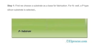
  • 1. Step 1: First we choose a substrate as a base for fabrication. For N- well, a P-type silicon substrate is selected.
  • 2. Step 2 – Oxidation: The selective diffusion of n-type impurities is accomplished using SiO2 as a barrier which protects portions of the wafer against contamination of the substrate. SiO2 is laid out by oxidation process done exposing the substrate to high-quality oxygen and hydrogen in an oxidation chamber at approximately 10000c
  • 3. Step 3 – Growing of Photoresist: At this stage to permit the selective etching, the SiO2 layer is subjected to the photolithography process. In this process, the wafer is coated with a uniform film of a photosensitive emulsion.
  • 4. Step 4 – Masking: This step is the continuation of the photolithography process. In this step, a desired pattern of openness is made using a stencil. This stencil is used as a mask over the photoresist. The substrate is now exposed to UV rays the photoresist present under the exposed regions of mask gets polymerized.
  • 5. Step 5 – Removal of Unexposed Photoresist: The mask is removed and the unexposed region of photoresist is dissolved by developing wafer using a chemical such as Trichloroethylene.
  • 6. Step 6 – Etching: The wafer is immersed in an etching solution of hydrofluoric acid, which removes the oxide from the areas through which dopants are to be diffused.
  • 7. Step 7 – Removal of Whole Photoresist Layer: During the etching process, those portions of SiO2 which are protected by the photoresist layer are not affected. The photoresist mask is now stripped off with a chemical solvent (hot H2SO4)
  • 8. Step 8 – Formation of N-well: The n-type impurities are diffused into the p-type substrate through the exposed region thus forming an N- well.
  • 9. Step 9 – Removal of SiO2: The layer of SiO2 is now removed by using hydrofluoric acid.
  • 10. Step 10 – Deposition of Polysilicon: The misalignment of the gate of a CMOS transistor would lead to the unwanted capacitance which could harm circuit. So to prevent this “Self-aligned gate process” is preferred where gate regions are formed before the formation of source and drain using ion implantation.
  • 11. Polysilicon is used for formation of the gate because it can withstand the high temperature greater than 80000c when a wafer is subjected to annealing methods for formation of source and drain. Polysilicon is deposited by using Chemical Deposition Process over a thin layer of gate oxide. This thin gate oxide under the Polysilicon layer prevents further doping under the gate region.
  • 12. Step 11 – Formation of Gate Region: Except the two regions required for formation of the gate for NMOS and PMOS transistors the remaining portion of Polysilicon is stripped off.
  • 13. Step 12 – Oxidation Process: An oxidation layer is deposited over the wafer which acts as a shield for further diffusion and metallization processes.
  • 14. Step 13 – Masking and Diffusion: For making regions for diffusion of n-type impurities using masking process small gaps are made.
  • 15. Using diffusion process three n+ regions are developed for the formation of terminals of NMOS.
  • 16. Step 14 – Removal of Oxide: The oxide layer is stripped off.
  • 17. Step 15 – P-type Diffusion: Similar to the n-type diffusion for forming the terminals of PMOS p-type diffusion are carried out.
  • 18. Step 16 – Laying of Thick Field oxide: Before forming the metal terminals a thick field oxide is laid out to form a protective layer for the regions of the wafer where no terminals are required.
  • 19. Step 17 – Metallization: This step is used for the formation of metal terminals which can provide interconnections. Aluminum is spread on the whole wafer.
  • 20. Step 18 – Removal of Excess Metal: The excess metal is removed from the wafer. Step 19 – Formation of Terminals: In the gaps formed after removal of excess metal terminals are formed for the interconnections.
  • 21. Step 20 – Assigning the Terminal Names: Names are assigned to the terminals of NMOS and PMOS transistors.