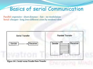
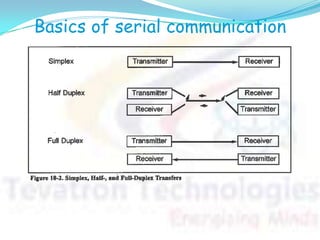
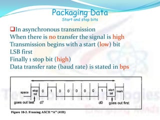
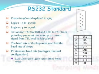
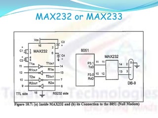
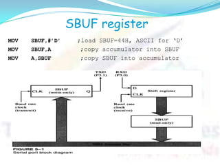
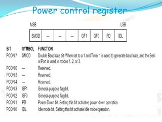
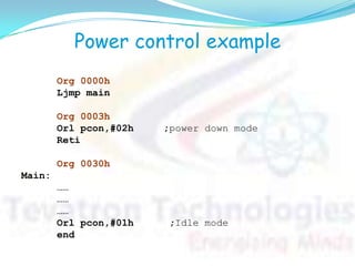
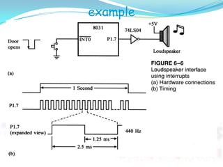
Presented by:-
Gaurav Saraswat
Associate Designing Engineer at Tevatron Technology
Basics of serial Communication
Parallel: expensive - short distance – fast – no modulation
Serial :cheaper– long (two different cities by modem)-slow
Basics of serial communication
Packaging Data
Start and stop bits
In asynchronous transmission
When there is no transfer the signal is high
Transmission begins with a start (low) bit
LSB first
Finally 1 stop bit (high)
Data transfer rate (baud rate) is stated in bps
RS232 Standard
1 DCD
2 RD
3 TD
4 DTR
5 GND
6 DSR
7 RTS
8 CTS
9 RI
 Create in 1960 and updated in 1969
 Logic 1 : -3 to -25 volt
 Logic 0 : 3 to 25 volt
 To Connect TXD to RXD and RXD to TXD from
pc to 8051 you must use max232 to convert
signal from TTL level to RS232 level
 The baud rate of the 8051 must matched the
baud rate of the pc
 PC standard baud rate (see hyper terminal
configuration)
 2400-4800-9600-14400-19200-28800-33600-
57600
MAX232 or MAX233
SBUF register
MOV SBUF,#’D’ ;load SBUF=44H, ASCII for ‘D’
MOV SBUF,A ;copy accumulator into SBUF
MOV A,SBUF ;copy SBUF into accumulator
Serial control (SCON) Register
SM2 : used for multi processor communication
REN : receive enable (by software enable/disable)
TB8 : transmit bit8
RB8 : receive bit 8
TI : transmit interrupt flag set by HW after send , clear by SW
RI : receive interrupt flag set by HW after received ,clear by SW
SM0 RITIRB8TB8RENSM2SM1
7 6 5 4 3 2 1 0
SM0 SM1 MODE operation transmit rate
0 0 0 shift register fixed (xtal/12)
0 1 1 8 bit UART variable (timer1)
1 0 2 9 bit UART fixed (xtal/32 or xtal/64)
1 1 3 9 bit UART variable (timer1)
SM0 : mode specifier
SM1 : mode specifier
Mode of operation
 Mode 0 :
 Serial data enters and exits through RxD
 TxD outputs the shift clock.
 8 bits are transmitted/received(LSB first)
 The baud rate is fixed a 1/12 the oscillator frequency.
 Application
 Port expansion
8051
TXD
RXD Shift register
clk
data
Timing of send in mode 0
One machine cycle
oscillator cycle
RXD (data)
TXD (clock pulse)
MOV SCON,#0001xxxxB
Wait: JNB RI,WAIT
CLR RI
MOV A,SBUF
MOV SCON,#0001xxxxB
Wait: JNB TI,WAIT
CLR TI
MOV SBUF,A
Mode of operation
 Mode 1
 Ten bits are transmitted (through TxD) or received (through RxD)
(A start bit (0), 8 data bits (LSB first), and a stop bit (1) )
 On receive, the stop bit goes into RB8 in SCON
 the baud rate is determined by the Timer 1 overflow rate.
 Timer1 clock is 1/32 machine cycle (MC=1/12 XTAL)
• Timer clock can be programmed as 1/16 of machine cycle
• Transmission is initiated by any instruction that uses SBUF as a
destination register.
Timer
modes
GATE C/T M1 M0 GATE C/T M1 M0
Timer 1 Timer 0
(MSB) (LSB)
Programming for sending data
( in mode 1 )
4. SETB TR1
5. MOV SBUF, DATA
6. WAIT: JNB TI,WAIT
7. CLR TI
BAUD RATE VALUE IN TH VALUE IN HEX
9600 -3 FD
4800 -6 FA
2400 -12 F4
1200 -24 E8
XTAL=11.0592 MHz
GATE C/T M1 M0 GATE C/T M1 M0
Timer 1 Timer 0
(MSB
)
(LSB)1. MOV TMOD,#20H
2. MOV TH1,# baud rate
3. MOV SCON,#50H
SM0 RITIRB8TB8RENSM2SM1
Programming for sending data
( in mode 1 )
MOV TMOD,#20H ;TIMER 1 MODE 2
MOV TH1,#-3 ;9600 BAUD
MOV SCON,#50H ;REN enable
SETB TR1 ;start timer1
AGAIN: MOV SBUF, # “A”
WAIT: JNB TI,WAIT
CLR TI
SJMP AGAIN
Serial example(1)
Programming for recieving data
( in mode 1 )
MOV TMOD,#20H ;TIMER 1 MODE 2
MOV TH1,#-3 ;9600 BAUD
MOV SCON,#50H ;REN enable
SETB TR1 ;start timer1
WAIT: JNB RI,WAIT
MOV A,SBUF
CLR RI
SJMP WAIT
Serial example(2)
Mode of operation
 Mode 2 :
 Eleven bits are transmitted (through TxD), received (through RxD)
 A start bit (0)
 8 data bits (LSB first)
 A programmable 9th data bit
 and a stop bit (1)
 On transmit, the 9th bit (TB8) can be assigned 0 or 1.
 On receive, the 9the data bit goes into RB8 in SCON.
 the 9th can be parity bit
 The baud rate is programmable to 1/32 or 1/64 the oscillator frequency in
Mode 2 by SMOD bit in PCON register
 Mode 3
 Same as mode 2
 But may have a variable baud rate generated from Timer 1.
Mode of operation
What is SMOD
 Bit 7 of PCON register
 If SMOD=1 double baud rate
 PCON is not bit addressable
 How to set SMOD
Mov a, pcon
Setb acc.7
Mov pcon,a
Power control register
Power control
 A standard for applications where power consumption
is critical
 two power reducing modes
 Idle
 Power down
Idle mode
 An instruction that sets PCON.0 causes Idle mode
 Last instruction executed before going into the Idle mode
 the internal CPU clock is gated off
 Interrupt, Timer, and Serial Port functions act normally.
 All of registers , ports and internal RAM maintain their data during Idle
 ALE and PSEN hold at logic high levels
 Any interrupt
 will cause PCON.0 to be cleared by HW (terminate Idle mode)
 then execute ISR
 with RETI return and execute next instruction after Idle instruction.
 RST signal clears the IDL bit directly
Power-Down Mode
 An instruction that sets PCON.1 causes power dowm mode
 Last instruction executed before going into the power down
mode
 the on-chip oscillator is stopped.
 all functions are stopped,the contents of the on-chip RAM
and Special Function Registers are maintained.
 The ALE and PSEN output are held low
 The reset that terminates Power Down
Power control example
Org 0000h
Ljmp main
Org 0003h
Orl pcon,#02h ;power down mode
Reti
Org 0030h
Main:
……
……
……
Orl pcon,#01h ;Idle mode
end
example
Sereial com. ppt

Sereial com. ppt

  • 1.
    Presented by:- Gaurav Saraswat AssociateDesigning Engineer at Tevatron Technology
  • 2.
    Basics of serialCommunication Parallel: expensive - short distance – fast – no modulation Serial :cheaper– long (two different cities by modem)-slow
  • 3.
    Basics of serialcommunication
  • 4.
    Packaging Data Start andstop bits In asynchronous transmission When there is no transfer the signal is high Transmission begins with a start (low) bit LSB first Finally 1 stop bit (high) Data transfer rate (baud rate) is stated in bps
  • 5.
    RS232 Standard 1 DCD 2RD 3 TD 4 DTR 5 GND 6 DSR 7 RTS 8 CTS 9 RI  Create in 1960 and updated in 1969  Logic 1 : -3 to -25 volt  Logic 0 : 3 to 25 volt  To Connect TXD to RXD and RXD to TXD from pc to 8051 you must use max232 to convert signal from TTL level to RS232 level  The baud rate of the 8051 must matched the baud rate of the pc  PC standard baud rate (see hyper terminal configuration)  2400-4800-9600-14400-19200-28800-33600- 57600
  • 6.
  • 7.
    SBUF register MOV SBUF,#’D’;load SBUF=44H, ASCII for ‘D’ MOV SBUF,A ;copy accumulator into SBUF MOV A,SBUF ;copy SBUF into accumulator
  • 8.
    Serial control (SCON)Register SM2 : used for multi processor communication REN : receive enable (by software enable/disable) TB8 : transmit bit8 RB8 : receive bit 8 TI : transmit interrupt flag set by HW after send , clear by SW RI : receive interrupt flag set by HW after received ,clear by SW SM0 RITIRB8TB8RENSM2SM1 7 6 5 4 3 2 1 0 SM0 SM1 MODE operation transmit rate 0 0 0 shift register fixed (xtal/12) 0 1 1 8 bit UART variable (timer1) 1 0 2 9 bit UART fixed (xtal/32 or xtal/64) 1 1 3 9 bit UART variable (timer1) SM0 : mode specifier SM1 : mode specifier
  • 9.
    Mode of operation Mode 0 :  Serial data enters and exits through RxD  TxD outputs the shift clock.  8 bits are transmitted/received(LSB first)  The baud rate is fixed a 1/12 the oscillator frequency.  Application  Port expansion 8051 TXD RXD Shift register clk data
  • 10.
    Timing of sendin mode 0 One machine cycle oscillator cycle RXD (data) TXD (clock pulse) MOV SCON,#0001xxxxB Wait: JNB RI,WAIT CLR RI MOV A,SBUF MOV SCON,#0001xxxxB Wait: JNB TI,WAIT CLR TI MOV SBUF,A
  • 11.
    Mode of operation Mode 1  Ten bits are transmitted (through TxD) or received (through RxD) (A start bit (0), 8 data bits (LSB first), and a stop bit (1) )  On receive, the stop bit goes into RB8 in SCON  the baud rate is determined by the Timer 1 overflow rate.  Timer1 clock is 1/32 machine cycle (MC=1/12 XTAL) • Timer clock can be programmed as 1/16 of machine cycle • Transmission is initiated by any instruction that uses SBUF as a destination register.
  • 12.
    Timer modes GATE C/T M1M0 GATE C/T M1 M0 Timer 1 Timer 0 (MSB) (LSB)
  • 14.
    Programming for sendingdata ( in mode 1 ) 4. SETB TR1 5. MOV SBUF, DATA 6. WAIT: JNB TI,WAIT 7. CLR TI BAUD RATE VALUE IN TH VALUE IN HEX 9600 -3 FD 4800 -6 FA 2400 -12 F4 1200 -24 E8 XTAL=11.0592 MHz GATE C/T M1 M0 GATE C/T M1 M0 Timer 1 Timer 0 (MSB ) (LSB)1. MOV TMOD,#20H 2. MOV TH1,# baud rate 3. MOV SCON,#50H SM0 RITIRB8TB8RENSM2SM1
  • 15.
    Programming for sendingdata ( in mode 1 ) MOV TMOD,#20H ;TIMER 1 MODE 2 MOV TH1,#-3 ;9600 BAUD MOV SCON,#50H ;REN enable SETB TR1 ;start timer1 AGAIN: MOV SBUF, # “A” WAIT: JNB TI,WAIT CLR TI SJMP AGAIN Serial example(1)
  • 16.
    Programming for recievingdata ( in mode 1 ) MOV TMOD,#20H ;TIMER 1 MODE 2 MOV TH1,#-3 ;9600 BAUD MOV SCON,#50H ;REN enable SETB TR1 ;start timer1 WAIT: JNB RI,WAIT MOV A,SBUF CLR RI SJMP WAIT Serial example(2)
  • 17.
    Mode of operation Mode 2 :  Eleven bits are transmitted (through TxD), received (through RxD)  A start bit (0)  8 data bits (LSB first)  A programmable 9th data bit  and a stop bit (1)  On transmit, the 9th bit (TB8) can be assigned 0 or 1.  On receive, the 9the data bit goes into RB8 in SCON.  the 9th can be parity bit  The baud rate is programmable to 1/32 or 1/64 the oscillator frequency in Mode 2 by SMOD bit in PCON register  Mode 3  Same as mode 2  But may have a variable baud rate generated from Timer 1.
  • 18.
  • 19.
    What is SMOD Bit 7 of PCON register  If SMOD=1 double baud rate  PCON is not bit addressable  How to set SMOD Mov a, pcon Setb acc.7 Mov pcon,a
  • 20.
  • 21.
    Power control  Astandard for applications where power consumption is critical  two power reducing modes  Idle  Power down
  • 22.
    Idle mode  Aninstruction that sets PCON.0 causes Idle mode  Last instruction executed before going into the Idle mode  the internal CPU clock is gated off  Interrupt, Timer, and Serial Port functions act normally.  All of registers , ports and internal RAM maintain their data during Idle  ALE and PSEN hold at logic high levels  Any interrupt  will cause PCON.0 to be cleared by HW (terminate Idle mode)  then execute ISR  with RETI return and execute next instruction after Idle instruction.  RST signal clears the IDL bit directly
  • 23.
    Power-Down Mode  Aninstruction that sets PCON.1 causes power dowm mode  Last instruction executed before going into the power down mode  the on-chip oscillator is stopped.  all functions are stopped,the contents of the on-chip RAM and Special Function Registers are maintained.  The ALE and PSEN output are held low  The reset that terminates Power Down
  • 24.
    Power control example Org0000h Ljmp main Org 0003h Orl pcon,#02h ;power down mode Reti Org 0030h Main: …… …… …… Orl pcon,#01h ;Idle mode end
  • 25.