The document discusses interfacing a microcontroller with various peripherals including timers, serial communication, interrupts, LCDs, and keyboards. It provides details on:
- Programming timers in 8051 microcontrollers for time delays and waveform generation.
- Serial communication protocols including asynchronous communication and RS-232 standards.
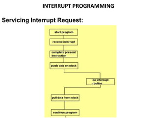
- Configuring and handling interrupts from different sources and writing interrupt service routines.
- Interfacing 8051 with LCDs for display and matrix keyboards for input using specific I/O ports for scanning rows and columns.


![LCD and Keyboard
Interfacing
1.P1 as an I/P port for microcontroller 8051, port P0 as an O/P port of
microcontroller 8051 and port P2 is used for displaying the number of
pressed key.
2.Make all rows of port P0 high so that it gives high signal when key is pressed.
3.See if any key is pressed by scanning the port P1 by checking all columns for
non zero condition.
4. Initiate a counter to hold the count so that each key is counted.
5. Check port P1 for nonzero condition. If any nonzero number is there in
[accumulator], start column scanning by following step 9.
6. Otherwise make next row high in port P1.
7.Add a count of 08h to the counter to move to the next row by repeating steps
from step 6.
8.If any key pressed is found, the [accumulator] content is rotated right through
the carry until carry bit sets, while doing this increment the count in the
counter till carry is found.
9.Move the content in the counter to display in data field or to memory
location
10. To repeat the procedures go to step 2.](https://image.slidesharecdn.com/ec8691-unit5-230831011102-7c35061f/85/EC8691-UNIT-5-pdf-52-320.jpg)