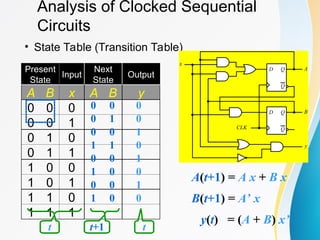
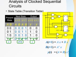
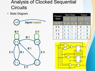
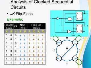
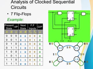
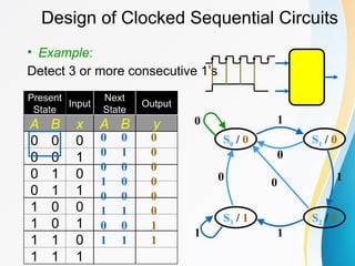
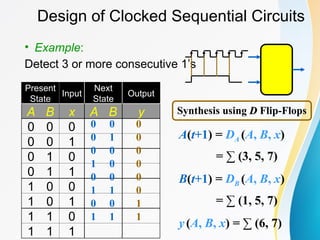
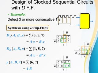
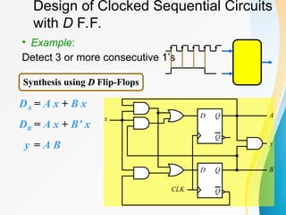
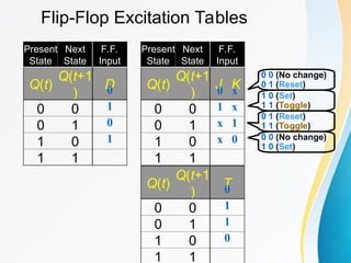
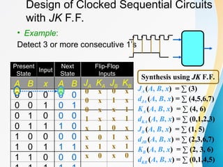
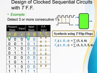
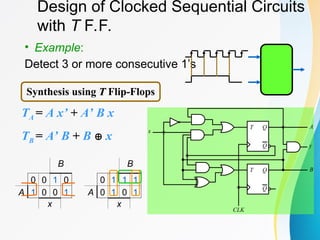
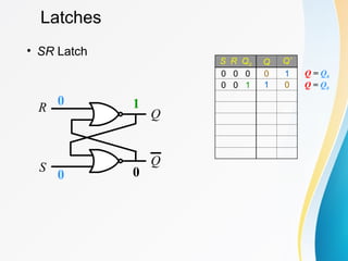
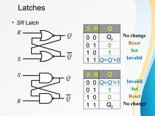
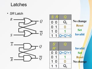
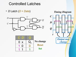
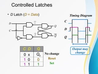
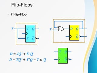
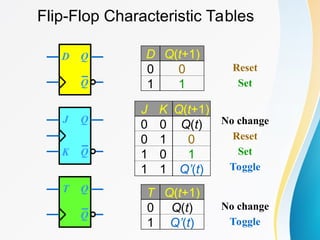
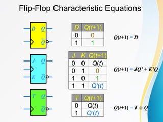
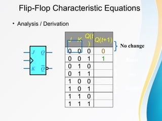
Sequential
Circuits
2
Sequential Circuits
Combinational
Circuit
Memory
Elements
Inputs Outputs
• Asynchronous
• Synchronous
Combinational
Circuit
Flip-flops
Inputs Outputs
Clock
Latches
• SR Latch
R
S
Q
Q
S R Q0 Q Q’
0 0 0
0
1
0
0
0 1 Q = Q0
Initial Value
Latches
• SR Latch
R
S
Q
Q
S R Q0 Q Q’
0 0 0 0 1
0 0 1
1
0
0
0
1 0 Q = Q0
Q = Q0
Latches
• SR Latch
R
S
Q
Q
S R Q0 Q Q’
0 0 0 0 1
0 0 1 1 0
0 1 0 0
0
1
1
0
1 Q = 0
Q = Q0
Latches
• SR Latch
R
S
Q
Q
S R Q0 Q Q’
0 0 0 0 1
0 0 1 1 0
0 1 0 0 1
0 1 1
1
0
1
0
0 1
Q = 0
Q = Q0
Q = 0
Latches
• SR Latch
R
S
Q
Q
S R Q0 Q Q’
0 0 0 0 1
0 0 1 1 0
0 1 0 0 1
0 1 1 0 1
1 0 0
0
1
0
1
1 0
Q = 0
Q = Q0
Q = 1
Latches
• SR Latch
R
S
Q
Q
S R Q0 Q Q’
0 0 0 0 1
0 0 1 1 0
0 1 0 0 1
0 1 1 0 1
1 0 0 1 0
1 0 1
1
0
0
1
1 0
Q = 0
Q = Q0
Q = 1
Q = 1
Latches
• SR Latch
R
S
Q
Q
S R Q0 Q Q’
0 0 0 0 1
0 0 1 1 0
0 1 0 0 1
0 1 1 0 1
1 0 0 1 0
1 0 1 1 0
1 1 0
0
1
1
1
0 0
Q = 0
Q = Q0
Q = 1
Q = Q’
0
Latches
• SR Latch
R
S
Q
Q
S R Q0 Q Q’
0 0 0 0 1
0 0 1 1 0
0 1 0 0 1
0 1 1 0 1
1 0 0 1 0
1 0 1 1 0
1 1 0 0 0
1 1 1
1
0
1
1
0 0
Q = 0
Q = Q0
Q = 1
Q = Q’
0
Q = Q’
Latches
• SR Latch
R
S
Q
Q
S R Q
0 0 Q0
0 1 0
1 0 1
1 1 Q=Q’=0
No change
Reset
Set
Invalid
S
R
Q
Q
S R Q
0 0 Q=Q’=1
0 1 1
1 0 0
1 1 Q0
Invalid
Set
Reset
No change
Latches
• SR Latch
R
S
Q
Q
S R Q
0 0 Q0
0 1 0
1 0 1
1 1 Q=Q’=0
No change
Reset
Set
Invalid
S’
R’
Q
0 0 Q=Q’=1
0 1 1
1 0 0
1 1 Q0
Invalid
Set
Reset
No change
S
R
Q
Q
Controlled Latches
• SR Latch with Control Input
C S R Q
0 x x Q0
1 0 0 Q0
1 0 1 0
1 1 0 1
1 1 1 Q=Q’
No change
No change
Reset
Set
Invalid
S
R
Q
Q
S
R
C
S
R
Q
Q
S
R
C
Controlled Latches
• D Latch (D = Data)
C D Q
0 x Q0
1 0 0
1 1 1
No change
Reset
Set
S
R
Q
Q
D
C
C
Timing Diagram
D
Q
t
Output may
change
Controlled Latches
• D Latch (D = Data)
C D Q
0 x Q0
1 0 0
1 1 1
No change
Reset
Set
C
Timing Diagram
D
Q
Output may
change
S
R
Q
Q
D
C
Flip-Flops
• Controlled latches are level-triggered
• Flip-Flops are edge-triggered
C
CLK Positive Edge
CLK Negative Edge
Flip-Flops
• Master-Slave D Flip-Flop
D Latch
(Master)
D
C
Q
D Latch
(Slave)
D
C
Q Q
D
CLK
CLK
D
QMaster
QSlave
Looks like it is negative
edge-triggered
Master Slave
Flip-Flops
• Edge-Triggered D Flip-Flop
D
CLK
Q
Q
D Q
Q
D Q
Q
Positive
Edge
Negative Edge
Flip-Flops
• JK Flip-Flop
D Q
Q
Q
Q
CLK
J
K
J Q
Q
K
D = JQ’ + K’Q
Flip-Flops
• T Flip-Flop
D = TQ’ + T’Q = T  Q
J Q
Q
K
T D Q
Q
T
D = JQ’ + K’Q
T Q
Q
Flip-Flop Characteristic Tables
D Q
Q
D Q(t+1)
0 0
1 1
Reset
Set
J K Q(t+1)
0 0 Q(t)
0 1 0
1 0 1
1 1 Q’(t)
No change
Reset
Set
Toggle
J Q
Q
K
T Q
Q
T Q(t+1)
0 Q(t)
1 Q’(t)
No change
Toggle
Flip-Flop Characteristic Equations
D Q
Q
D Q(t+1)
0 0
1 1
Q(t+1) = D
J K Q(t+1)
0 0 Q(t)
0 1 0
1 0 1
1 1 Q’(t)
Q(t+1) = JQ’ + K’Q
J Q
Q
K
T Q
Q
T Q(t+1)
0 Q(t)
1 Q’(t)
Q(t+1) = T  Q
Flip-Flop Characteristic Equations
• Analysis / Derivation
J Q
Q
K
J K
Q(t
)
Q(t+1)
0 0 0 0
0 0 1 1
0 1 0
0 1 1
1 0 0
1 0 1
1 1 0
1 1 1
No change
Reset
Set
Toggle
Flip-Flop Characteristic Equations
• Analysis / Derivation
J Q
Q
K
J K
Q(t
)
Q(t+1)
0 0 0 0
0 0 1 1
0 1 0 0
0 1 1 0
1 0 0
1 0 1
1 1 0
1 1 1
No change
Reset
Set
Toggle
Flip-Flop Characteristic Equations
• Analysis / Derivation
J Q
Q
K
J K
Q(t
)
Q(t+1)
0 0 0 0
0 0 1 1
0 1 0 0
0 1 1 0
1 0 0 1
1 0 1 1
1 1 0
1 1 1
No change
Reset
Set
Toggle
Flip-Flop Characteristic Equations
• Analysis / Derivation
J Q
Q
K
J K
Q(t
)
Q(t+1)
0 0 0 0
0 0 1 1
0 1 0 0
0 1 1 0
1 0 0 1
1 0 1 1
1 1 0 1
1 1 1 0
No change
Reset
Set
Toggle
Flip-Flop Characteristic Equations
• Analysis / Derivation
J Q
Q
K
J K
Q(t
)
Q(t+1)
0 0 0 0
0 0 1 1
0 1 0 0
0 1 1 0
1 0 0 1
1 0 1 1
1 1 0 1
1 1 1 0
K
0 1 0 0
J 1 1 0 1
Q
Q(t+1) = JQ’ + K’Q
Flip-Flops with Direct Inputs
• Asynchronous Reset
D Q
Q
R
Reset
R’ D CLK Q(t+1)
0 x x 0
Flip-Flops with Direct Inputs
• Asynchronous Reset
D Q
Q
R
Reset
R’ D CLK Q(t+1)
0 x x 0
1 0 ↑ 0
1 1 ↑ 1
Flip-Flops with Direct Inputs
• Asynchronous Preset and Clear
PR’CLR’ D CLK Q(t+1)
1 0 x x 0
D Q
Q
CLR
Reset
PR
Preset
Flip-Flops with Direct Inputs
• Asynchronous Preset and Clear
PR’CLR’ D CLK Q(t+1)
1 0 x x 0
0 1 x x 1
D Q
Q
CLR
Reset
PR
Preset
Flip-Flops with Direct Inputs
• Asynchronous Preset and Clear
PR’CLR’ D CLK Q(t+1)
1 0 x x 0
0 1 x x 1
1 1 0 ↑ 0
1 1 1 ↑ 1
D Q
Q
CLR
Reset
PR
Preset
Analysis of Clocked Sequential
Circuits
• The State
– State = Values of all Flip-Flops
Example
A B = 0 0
D Q
Q
CLK
D Q
Q
A
B
y
x
Analysis of Clocked Sequential
Circuits
• State Equations
D Q
Q
CLK
D Q
Q
A
B
y
x
A(t+1) = DA
= A(t) x(t)+B(t) x(t)
= A x + B x
B(t+1) = DB
= A’(t) x(t)
= A’ x
y(t) = [A(t)+ B(t)] x’(t)
= (A + B) x’
Analysis of Clocked Sequential
Circuits
• State Table (Transition Table)
D Q
Q
CLK
D Q
Q
A
B
y
x
A(t+1) = A x + B x
B(t+1) = A’ x
y(t) = (A + B) x’
Present
State
Input
Next
State
Output
A B x A B y
0 0 0
0 0 1
0 1 0
0 1 1
1 0 0
1 0 1
1 1 0
1 1 1
t+1 t
t
0 0 0
0 1 0
0 0 1
1 1 0
0 0 1
1 0 0
0 0 1
1 0 0
Analysis of Clocked Sequential
Circuits
• State Table (Transition Table)
D Q
Q
CLK
D Q
Q
A
B
y
x
A(t+1) = A x + B x
B(t+1) = A’ x
y(t) = (A + B) x’
Present
State
Next State Output
x = 0 x = 1 x = 0 x = 1
A B A B A B y y
0 0 0 0 0 1 0 0
0 1 0 0 1 1 1 0
1 0 0 0 1 0 1 0
1 1 0 0 1 0 1 0
t+1 t
t
Analysis of Clocked Sequential
Circuits
• State Diagram
D Q
Q
CLK
D Q
Q
A
B
y
x
0 0 1 0
0 1 1 1
0/0
0/1
1/0
1/0
1/0
1/0 0/1
0/1
AB input/output
Present
State
Next State Output
x = 0 x = 1 x = 0 x = 1
A B A B A B y y
0 0 0 0 0 1 0 0
0 1 0 0 1 1 1 0
1 0 0 0 1 0 1 0
1 1 0 0 1 0 1 0
Analysis of Clocked Sequential
Circuits
• D Flip-Flops
Example: D Q
Q
x
CLK
y
A
Present
State
Input
Next
State
A x y A
0 0 0
0 0 1
0 1 0
0 1 1
1 0 0
1 0 1
1 1 0
1 1 1
0
1
1
0
1
0
0
1
0 1
00,11 00,11
01,10
01,10
A(t+1) = DA = A  x  y
Analysis of Clocked Sequential
Circuits
• JK Flip-Flops
Example:
J Q
Q
K
CLK
J Q
Q
K
x
A
B
JA = B KA = B x’
JB = x’ KB = A  x
A(t+1) = JA Q’A + K’A QA
= A’B + AB’ + Ax
B(t+1) = JB Q’B + K’B QB
= B’x’ + ABx + A’Bx’
Present
State
I/P
Next
State
Flip-Flop
Inputs
A B x A B JA KA JB KB
0 0 0
0 0 1
0 1 0
0 1 1
1 0 0
1 0 1
1 1 0
1 1 1
0 0 1 0
0 0 0 1
1 1 1 0
1 0 0 1
0 0 1 1
0 0 0 0
1 1 1 1
1 0 0 0
0 1
0 0
1 1
1 0
1 1
1 0
0 0
1 1
Analysis of Clocked Sequential
Circuits
• JK Flip-Flops
Example:
J Q
Q
K
CLK
J Q
Q
K
x
A
B
Present
State
I/P
Next
State
Flip-Flop
Inputs
A B x A B JA KA JB KB
0 0 0
0 0 1
0 1 0
0 1 1
1 0 0
1 0 1
1 1 0
1 1 1
0 0 1 0
0 0 0 1
1 1 1 0
1 0 0 1
0 0 1 1
0 0 0 0
1 1 1 1
1 0 0 0
0 1
0 0
1 1
1 0
1 1
1 0
0 0
1 1
0 0 1 1
0 1 1 0
1 0 1
0
1
0
0
1
Analysis of Clocked Sequential
Circuits
• T Flip-Flops
Example:
TA = B x TB = x
y = A B
A(t+1) = TA Q’A + T’A QA
= AB’ + Ax’ + A’Bx
B(t+1) = TB Q’B + T’B QB
= x  B
A
B
T Q
Q
R
T Q
Q
R
CLK Reset
x
y
Present
State
I/P
Next
State
F.F
Inputs
O/P
A B x A B TA TB y
0 0 0
0 0 1
0 1 0
0 1 1
1 0 0
1 0 1
1 1 0
1 1 1
0 0
0 1
0 0
1 1
0 0
0 1
0 0
1 1
0 0
0 1
0 1
1 0
1 0
1 1
1 1
0 0
0
0
0
0
0
0
1
1
Analysis of Clocked Sequential
Circuits
• T Flip-Flops
Example:
A
B
T Q
Q
R
T Q
Q
R
CLK Reset
x
y
Present
State
I/P
Next
State
F.F
Inputs
O/P
A B x A B TA TB y
0 0 0
0 0 1
0 1 0
0 1 1
1 0 0
1 0 1
1 1 0
1 1 1
0 0
0 1
0 0
1 1
0 0
0 1
0 0
1 1
0 0
0 1
0 1
1 0
1 0
1 1
1 1
0 0
0
0
0
0
0
0
1
1
0 0 0 1
1 1 1 0
0/0
1/0
0/0
1/0
1/0
1/1
0/0
0/1
Mealy and Moore Models
• The Mealy model: the outputs are
functions of both the present state and
inputs .
– The outputs may change if the inputs change
during the clock pulse period.
• The outputs may have momentary false values
unless the inputs are synchronized with the clocks.
• The Moore model: the outputs are
functions of the present state only.
– The outputs are synchronous with the clocks.
Mealy and Moore Models
Block diagram of Mealy and Moore state machine
Mealy and Moore Models
Present
State
I/P
Next
State
O/P
A B x A B y
0 0 0 0 0 0
0 0 1 0 1 0
0 1 0 0 0 1
0 1 1 1 1 0
1 0 0 0 0 1
1 0 1 1 0 0
1 1 0 0 0 1
1 1 1 1 0 0
Mealy
Mealy
For the same state
state,
the output
output changes with the input
input
Present
State
I/P
Next
State
O/P
A B x A B y
0 0 0 0 0 0
0 0 1 0 1 0
0 1 0 0 1 0
0 1 1 1 0 0
1 0 0 1 0 0
1 0 1 1 1 0
1 1 0 1 1 1
1 1 1 0 0 1
Moore
Moore
For the same state
state,
the output
output does not change with the input
input
Moore State Diagram
State / Output
0 0 / 0 0 1 / 0
1 1 / 1 1 0 / 0
0
1
1
1
0
0
0
1
State Reduction and Assignment
• State Reduction
Reductions on the
number of flip-flops and
the number of gates.
– A reduction in the
number of states may
result in a reduction in
the number of flip-flops.
– An example state
diagram showing in Fig.
5.25.
Fig. 5.25 State diagram
State Reduction
– Only the input-output
sequences are
important.
– Two circuits are
equivalent
• Have identical outputs for
all input sequences;
• The number of states is
not important.
Fig. 5.25 State diagram
State: a a b c d e f f g f g a
Input: 0 1 0 1 0 1 1 0 1 0 0
Output: 0 0 0 0 0 1 1 0 1 0 0
• Equivalent states
– Two states are said to be equivalent
• For each member of the set of inputs, they give
exactly the same output and send the circuit to the
same state or to an equivalent state.
• One of them can be removed.
• Reducing the state table
– e = g (remove g);
– d = f (remove f);
– The reduced finite state machine
State: a a b c d e d d e d e a
Input: 0 1 0 1 0 1 1 0 1 0 0
Output: 0 0 0 0 0 1 1 0 1 0 0
– The checking of each pair
of states for possible
equivalence can be done
systematically using
Implication Table.
– The unused states are
treated as don't-care
condition  fewer
combinational gates.
Fig. 5.26 Reduced State diagram
Implication Table
State Assignment
• State Assignment
• To minimize the cost of the combinational
circuits.
– Three possible binary state assignments. (m
states need n-bits, where 2n
> m)
– Any binary number assignment is satisfactory
as long as each state is assigned a unique
number.
– Use binary assignment 1.
Design Procedure
• Design Procedure for sequential circuit
– The word description of the circuit behavior to
get a state diagram;
– State reduction if necessary;
– Assign binary values to the states;
– Obtain the binary-coded state table;
– Choose the type of flip-flops;
– Derive the simplified flip-flop input equations
and output equations;
– Draw the logic diagram;
Design of Clocked Sequential Circuits
• Example:
Detect 3 or more consecutive 1’s
S0 / 0 S1 / 0
S3 / 1 S2 / 0
0
1
1
0
0
1
0
1
State A B
S0 0 0
S1 0 1
S2 1 0
S3 1 1
Design of Clocked Sequential Circuits
• Example:
Detect 3 or more consecutive 1’s
Present
State
Input
Next
State
Output
A B x A B y
0 0 0
0 0 1
0 1 0
0 1 1
1 0 0
1 0 1
1 1 0
1 1 1
0 0 0
0 1 0
0 0 0
1 0 0
0 0 0
1 1 0
0 0 1
1 1 1
S0 / 0 S1 / 0
S3 / 1 S2 / 0
0
1
1
0 0
1
0
1
Design of Clocked Sequential Circuits
• Example:
Detect 3 or more consecutive 1’s
Present
State
Input
Next
State
Output
A B x A B y
0 0 0
0 0 1
0 1 0
0 1 1
1 0 0
1 0 1
1 1 0
1 1 1
0 0 0
0 1 0
0 0 0
1 0 0
0 0 0
1 1 0
0 0 1
1 1 1
A(t+1) = DA (A, B, x)
= ∑ (3, 5, 7)
B(t+1) = DB (A, B, x)
= ∑ (1, 5, 7)
y(A, B, x) = ∑ (6, 7)
Synthesis using D
D Flip-Flops
Design of Clocked Sequential Circuits
with D F.F.
• Example:
Detect 3 or more consecutive 1’s
DA (A, B, x) = ∑ (3, 5, 7)
= A x + B x
DB (A, B, x) = ∑ (1, 5, 7)
= A x + B’ x
y(A, B, x) = ∑ (6, 7)
= A B
Synthesis using D
D Flip-Flops
B
0 0 1 0
A 0 1 1 0
x B
0 1 0 0
A 0 1 1 0
x
B
0 0 0 0
A 0 0 1 1
x
Design of Clocked Sequential Circuits
with D F.F.
• Example:
Detect 3 or more consecutive 1’s
DA = A x + B x
DB = A x + B’ x
y = A B
Synthesis using D
D Flip-Flops
D Q
Q
A
CLK
x
B
D Q
Q
y
Flip-Flop Excitation Tables
Present
State
Next
State
F.F.
Input
Q(t)
Q(t+1
)
D
0 0
0 1
1 0
1 1
Present
State
Next
State
F.F.
Input
Q(t)
Q(t+1
)
J K
0 0
0 1
1 0
1 1
0 0 (No change)
0 1 (Reset)
0 x
1 x
x 1
x 0
0
1
0
1
1 0 (Set)
1 1 (Toggle)
0 1 (Reset)
1 1 (Toggle)
0 0 (No change)
1 0 (Set)
Q(t)
Q(t+1
)
T
0 0
0 1
1 0
1 1
0
1
1
0
Design of Clocked Sequential Circuits
with JK F.F.
• Example:
Detect 3 or more consecutive 1’s
Present
State
Input
Next
State
Flip-Flop
Inputs
A B x A B JA KA JB KB
0 0 0 0 0
0 0 1 0 1
0 1 0 0 0
0 1 1 1 0
1 0 0 0 0
1 0 1 1 1
1 1 0 0 0
0 x
0 x
0 x
1 x
x 1
x 0
x 1
x 0
JA (A, B, x) = ∑ (3)
dJA (A, B, x) = ∑ (4,5,6,7)
KA (A, B, x) = ∑ (4, 6)
dKA (A, B, x) = ∑ (0,1,2,3)
JB (A, B, x) = ∑ (1, 5)
dJB (A, B, x) = ∑ (2,3,6,7)
KB (A, B, x) = ∑ (2, 3, 6)
dKB (A, B, x) = ∑ (0,1,4,5)
Synthesis using JK
JK F.F.
0 x
1 x
x 1
x 1
0 x
1 x
x 1
x 0
Design of Clocked Sequential Circuits
with JK F.F.
• Example:
Detect 3 or more consecutive 1’s
JA = B x KA = x’
JB = x KB = A’ + x’
Synthesis using JK
JK Flip-Flops
B
0 0 1 0
A x x x x
x
B
x x x x
A 1 0 0 1
x
B
0 1 x x
A 0 1 x x
x
B
x x 1 1
A x x 0 1
x
CLK
J Q
Q
K
x
A
B
J Q
Q
K y
Design of Clocked Sequential Circuits
with T F.F.
• Example:
Detect 3 or more consecutive 1’s
Present
State
Input
Next
State
F.F.
Input
A B x A B TA TB
0 0 0 0 0
0 0 1 0 1
0 1 0 0 0
0 1 1 1 0
1 0 0 0 0
1 0 1 1 1
1 1 0 0 0
1 1 1 1 1
0
0
0
1
1
0
1
0
Synthesis using T
T Flip-Flops
0
1
1
1
0
1
1
0
TA (A, B, x) = ∑ (3, 4, 6)
TB (A, B, x) = ∑ (1, 2, 3, 5, 6)
Design of Clocked Sequential Circuits
with T F.F.
• Example:
Detect 3 or more consecutive 1’s
TA = A x’ + A’ B x
TB = A’ B + B  x
Synthesis using T
T Flip-Flops
B
0 0 1 0
A 1 0 0 1
x
B
0 1 1 1
A 0 1 0 1
x
A
B
y
T Q
Q
x
CLK
T Q
Q

CS6201_UNIT3_L01.ppt Digiital Electronics

  • 1.
  • 2.
    2 Sequential Circuits Combinational Circuit Memory Elements Inputs Outputs •Asynchronous • Synchronous Combinational Circuit Flip-flops Inputs Outputs Clock
  • 3.
    Latches • SR Latch R S Q Q SR Q0 Q Q’ 0 0 0 0 1 0 0 0 1 Q = Q0 Initial Value
  • 4.
    Latches • SR Latch R S Q Q SR Q0 Q Q’ 0 0 0 0 1 0 0 1 1 0 0 0 1 0 Q = Q0 Q = Q0
  • 5.
    Latches • SR Latch R S Q Q SR Q0 Q Q’ 0 0 0 0 1 0 0 1 1 0 0 1 0 0 0 1 1 0 1 Q = 0 Q = Q0
  • 6.
    Latches • SR Latch R S Q Q SR Q0 Q Q’ 0 0 0 0 1 0 0 1 1 0 0 1 0 0 1 0 1 1 1 0 1 0 0 1 Q = 0 Q = Q0 Q = 0
  • 7.
    Latches • SR Latch R S Q Q SR Q0 Q Q’ 0 0 0 0 1 0 0 1 1 0 0 1 0 0 1 0 1 1 0 1 1 0 0 0 1 0 1 1 0 Q = 0 Q = Q0 Q = 1
  • 8.
    Latches • SR Latch R S Q Q SR Q0 Q Q’ 0 0 0 0 1 0 0 1 1 0 0 1 0 0 1 0 1 1 0 1 1 0 0 1 0 1 0 1 1 0 0 1 1 0 Q = 0 Q = Q0 Q = 1 Q = 1
  • 9.
    Latches • SR Latch R S Q Q SR Q0 Q Q’ 0 0 0 0 1 0 0 1 1 0 0 1 0 0 1 0 1 1 0 1 1 0 0 1 0 1 0 1 1 0 1 1 0 0 1 1 1 0 0 Q = 0 Q = Q0 Q = 1 Q = Q’ 0
  • 10.
    Latches • SR Latch R S Q Q SR Q0 Q Q’ 0 0 0 0 1 0 0 1 1 0 0 1 0 0 1 0 1 1 0 1 1 0 0 1 0 1 0 1 1 0 1 1 0 0 0 1 1 1 1 0 1 1 0 0 Q = 0 Q = Q0 Q = 1 Q = Q’ 0 Q = Q’
  • 11.
    Latches • SR Latch R S Q Q SR Q 0 0 Q0 0 1 0 1 0 1 1 1 Q=Q’=0 No change Reset Set Invalid S R Q Q S R Q 0 0 Q=Q’=1 0 1 1 1 0 0 1 1 Q0 Invalid Set Reset No change
  • 12.
    Latches • SR Latch R S Q Q SR Q 0 0 Q0 0 1 0 1 0 1 1 1 Q=Q’=0 No change Reset Set Invalid S’ R’ Q 0 0 Q=Q’=1 0 1 1 1 0 0 1 1 Q0 Invalid Set Reset No change S R Q Q
  • 13.
    Controlled Latches • SRLatch with Control Input C S R Q 0 x x Q0 1 0 0 Q0 1 0 1 0 1 1 0 1 1 1 1 Q=Q’ No change No change Reset Set Invalid S R Q Q S R C S R Q Q S R C
  • 14.
    Controlled Latches • DLatch (D = Data) C D Q 0 x Q0 1 0 0 1 1 1 No change Reset Set S R Q Q D C C Timing Diagram D Q t Output may change
  • 15.
    Controlled Latches • DLatch (D = Data) C D Q 0 x Q0 1 0 0 1 1 1 No change Reset Set C Timing Diagram D Q Output may change S R Q Q D C
  • 16.
    Flip-Flops • Controlled latchesare level-triggered • Flip-Flops are edge-triggered C CLK Positive Edge CLK Negative Edge
  • 17.
    Flip-Flops • Master-Slave DFlip-Flop D Latch (Master) D C Q D Latch (Slave) D C Q Q D CLK CLK D QMaster QSlave Looks like it is negative edge-triggered Master Slave
  • 18.
    Flip-Flops • Edge-Triggered DFlip-Flop D CLK Q Q D Q Q D Q Q Positive Edge Negative Edge
  • 19.
    Flip-Flops • JK Flip-Flop DQ Q Q Q CLK J K J Q Q K D = JQ’ + K’Q
  • 20.
    Flip-Flops • T Flip-Flop D= TQ’ + T’Q = T  Q J Q Q K T D Q Q T D = JQ’ + K’Q T Q Q
  • 21.
    Flip-Flop Characteristic Tables DQ Q D Q(t+1) 0 0 1 1 Reset Set J K Q(t+1) 0 0 Q(t) 0 1 0 1 0 1 1 1 Q’(t) No change Reset Set Toggle J Q Q K T Q Q T Q(t+1) 0 Q(t) 1 Q’(t) No change Toggle
  • 22.
    Flip-Flop Characteristic Equations DQ Q D Q(t+1) 0 0 1 1 Q(t+1) = D J K Q(t+1) 0 0 Q(t) 0 1 0 1 0 1 1 1 Q’(t) Q(t+1) = JQ’ + K’Q J Q Q K T Q Q T Q(t+1) 0 Q(t) 1 Q’(t) Q(t+1) = T  Q
  • 23.
    Flip-Flop Characteristic Equations •Analysis / Derivation J Q Q K J K Q(t ) Q(t+1) 0 0 0 0 0 0 1 1 0 1 0 0 1 1 1 0 0 1 0 1 1 1 0 1 1 1 No change Reset Set Toggle
  • 24.
    Flip-Flop Characteristic Equations •Analysis / Derivation J Q Q K J K Q(t ) Q(t+1) 0 0 0 0 0 0 1 1 0 1 0 0 0 1 1 0 1 0 0 1 0 1 1 1 0 1 1 1 No change Reset Set Toggle
  • 25.
    Flip-Flop Characteristic Equations •Analysis / Derivation J Q Q K J K Q(t ) Q(t+1) 0 0 0 0 0 0 1 1 0 1 0 0 0 1 1 0 1 0 0 1 1 0 1 1 1 1 0 1 1 1 No change Reset Set Toggle
  • 26.
    Flip-Flop Characteristic Equations •Analysis / Derivation J Q Q K J K Q(t ) Q(t+1) 0 0 0 0 0 0 1 1 0 1 0 0 0 1 1 0 1 0 0 1 1 0 1 1 1 1 0 1 1 1 1 0 No change Reset Set Toggle
  • 27.
    Flip-Flop Characteristic Equations •Analysis / Derivation J Q Q K J K Q(t ) Q(t+1) 0 0 0 0 0 0 1 1 0 1 0 0 0 1 1 0 1 0 0 1 1 0 1 1 1 1 0 1 1 1 1 0 K 0 1 0 0 J 1 1 0 1 Q Q(t+1) = JQ’ + K’Q
  • 28.
    Flip-Flops with DirectInputs • Asynchronous Reset D Q Q R Reset R’ D CLK Q(t+1) 0 x x 0
  • 29.
    Flip-Flops with DirectInputs • Asynchronous Reset D Q Q R Reset R’ D CLK Q(t+1) 0 x x 0 1 0 ↑ 0 1 1 ↑ 1
  • 30.
    Flip-Flops with DirectInputs • Asynchronous Preset and Clear PR’CLR’ D CLK Q(t+1) 1 0 x x 0 D Q Q CLR Reset PR Preset
  • 31.
    Flip-Flops with DirectInputs • Asynchronous Preset and Clear PR’CLR’ D CLK Q(t+1) 1 0 x x 0 0 1 x x 1 D Q Q CLR Reset PR Preset
  • 32.
    Flip-Flops with DirectInputs • Asynchronous Preset and Clear PR’CLR’ D CLK Q(t+1) 1 0 x x 0 0 1 x x 1 1 1 0 ↑ 0 1 1 1 ↑ 1 D Q Q CLR Reset PR Preset
  • 33.
    Analysis of ClockedSequential Circuits • The State – State = Values of all Flip-Flops Example A B = 0 0 D Q Q CLK D Q Q A B y x
  • 34.
    Analysis of ClockedSequential Circuits • State Equations D Q Q CLK D Q Q A B y x A(t+1) = DA = A(t) x(t)+B(t) x(t) = A x + B x B(t+1) = DB = A’(t) x(t) = A’ x y(t) = [A(t)+ B(t)] x’(t) = (A + B) x’
  • 35.
    Analysis of ClockedSequential Circuits • State Table (Transition Table) D Q Q CLK D Q Q A B y x A(t+1) = A x + B x B(t+1) = A’ x y(t) = (A + B) x’ Present State Input Next State Output A B x A B y 0 0 0 0 0 1 0 1 0 0 1 1 1 0 0 1 0 1 1 1 0 1 1 1 t+1 t t 0 0 0 0 1 0 0 0 1 1 1 0 0 0 1 1 0 0 0 0 1 1 0 0
  • 36.
    Analysis of ClockedSequential Circuits • State Table (Transition Table) D Q Q CLK D Q Q A B y x A(t+1) = A x + B x B(t+1) = A’ x y(t) = (A + B) x’ Present State Next State Output x = 0 x = 1 x = 0 x = 1 A B A B A B y y 0 0 0 0 0 1 0 0 0 1 0 0 1 1 1 0 1 0 0 0 1 0 1 0 1 1 0 0 1 0 1 0 t+1 t t
  • 37.
    Analysis of ClockedSequential Circuits • State Diagram D Q Q CLK D Q Q A B y x 0 0 1 0 0 1 1 1 0/0 0/1 1/0 1/0 1/0 1/0 0/1 0/1 AB input/output Present State Next State Output x = 0 x = 1 x = 0 x = 1 A B A B A B y y 0 0 0 0 0 1 0 0 0 1 0 0 1 1 1 0 1 0 0 0 1 0 1 0 1 1 0 0 1 0 1 0
  • 38.
    Analysis of ClockedSequential Circuits • D Flip-Flops Example: D Q Q x CLK y A Present State Input Next State A x y A 0 0 0 0 0 1 0 1 0 0 1 1 1 0 0 1 0 1 1 1 0 1 1 1 0 1 1 0 1 0 0 1 0 1 00,11 00,11 01,10 01,10 A(t+1) = DA = A  x  y
  • 39.
    Analysis of ClockedSequential Circuits • JK Flip-Flops Example: J Q Q K CLK J Q Q K x A B JA = B KA = B x’ JB = x’ KB = A  x A(t+1) = JA Q’A + K’A QA = A’B + AB’ + Ax B(t+1) = JB Q’B + K’B QB = B’x’ + ABx + A’Bx’ Present State I/P Next State Flip-Flop Inputs A B x A B JA KA JB KB 0 0 0 0 0 1 0 1 0 0 1 1 1 0 0 1 0 1 1 1 0 1 1 1 0 0 1 0 0 0 0 1 1 1 1 0 1 0 0 1 0 0 1 1 0 0 0 0 1 1 1 1 1 0 0 0 0 1 0 0 1 1 1 0 1 1 1 0 0 0 1 1
  • 40.
    Analysis of ClockedSequential Circuits • JK Flip-Flops Example: J Q Q K CLK J Q Q K x A B Present State I/P Next State Flip-Flop Inputs A B x A B JA KA JB KB 0 0 0 0 0 1 0 1 0 0 1 1 1 0 0 1 0 1 1 1 0 1 1 1 0 0 1 0 0 0 0 1 1 1 1 0 1 0 0 1 0 0 1 1 0 0 0 0 1 1 1 1 1 0 0 0 0 1 0 0 1 1 1 0 1 1 1 0 0 0 1 1 0 0 1 1 0 1 1 0 1 0 1 0 1 0 0 1
  • 41.
    Analysis of ClockedSequential Circuits • T Flip-Flops Example: TA = B x TB = x y = A B A(t+1) = TA Q’A + T’A QA = AB’ + Ax’ + A’Bx B(t+1) = TB Q’B + T’B QB = x  B A B T Q Q R T Q Q R CLK Reset x y Present State I/P Next State F.F Inputs O/P A B x A B TA TB y 0 0 0 0 0 1 0 1 0 0 1 1 1 0 0 1 0 1 1 1 0 1 1 1 0 0 0 1 0 0 1 1 0 0 0 1 0 0 1 1 0 0 0 1 0 1 1 0 1 0 1 1 1 1 0 0 0 0 0 0 0 0 1 1
  • 42.
    Analysis of ClockedSequential Circuits • T Flip-Flops Example: A B T Q Q R T Q Q R CLK Reset x y Present State I/P Next State F.F Inputs O/P A B x A B TA TB y 0 0 0 0 0 1 0 1 0 0 1 1 1 0 0 1 0 1 1 1 0 1 1 1 0 0 0 1 0 0 1 1 0 0 0 1 0 0 1 1 0 0 0 1 0 1 1 0 1 0 1 1 1 1 0 0 0 0 0 0 0 0 1 1 0 0 0 1 1 1 1 0 0/0 1/0 0/0 1/0 1/0 1/1 0/0 0/1
  • 43.
    Mealy and MooreModels • The Mealy model: the outputs are functions of both the present state and inputs . – The outputs may change if the inputs change during the clock pulse period. • The outputs may have momentary false values unless the inputs are synchronized with the clocks. • The Moore model: the outputs are functions of the present state only. – The outputs are synchronous with the clocks.
  • 44.
    Mealy and MooreModels Block diagram of Mealy and Moore state machine
  • 45.
    Mealy and MooreModels Present State I/P Next State O/P A B x A B y 0 0 0 0 0 0 0 0 1 0 1 0 0 1 0 0 0 1 0 1 1 1 1 0 1 0 0 0 0 1 1 0 1 1 0 0 1 1 0 0 0 1 1 1 1 1 0 0 Mealy Mealy For the same state state, the output output changes with the input input Present State I/P Next State O/P A B x A B y 0 0 0 0 0 0 0 0 1 0 1 0 0 1 0 0 1 0 0 1 1 1 0 0 1 0 0 1 0 0 1 0 1 1 1 0 1 1 0 1 1 1 1 1 1 0 0 1 Moore Moore For the same state state, the output output does not change with the input input
  • 46.
    Moore State Diagram State/ Output 0 0 / 0 0 1 / 0 1 1 / 1 1 0 / 0 0 1 1 1 0 0 0 1
  • 47.
    State Reduction andAssignment • State Reduction Reductions on the number of flip-flops and the number of gates. – A reduction in the number of states may result in a reduction in the number of flip-flops. – An example state diagram showing in Fig. 5.25. Fig. 5.25 State diagram
  • 48.
    State Reduction – Onlythe input-output sequences are important. – Two circuits are equivalent • Have identical outputs for all input sequences; • The number of states is not important. Fig. 5.25 State diagram State: a a b c d e f f g f g a Input: 0 1 0 1 0 1 1 0 1 0 0 Output: 0 0 0 0 0 1 1 0 1 0 0
  • 49.
    • Equivalent states –Two states are said to be equivalent • For each member of the set of inputs, they give exactly the same output and send the circuit to the same state or to an equivalent state. • One of them can be removed.
  • 50.
    • Reducing thestate table – e = g (remove g); – d = f (remove f);
  • 51.
    – The reducedfinite state machine State: a a b c d e d d e d e a Input: 0 1 0 1 0 1 1 0 1 0 0 Output: 0 0 0 0 0 1 1 0 1 0 0
  • 52.
    – The checkingof each pair of states for possible equivalence can be done systematically using Implication Table. – The unused states are treated as don't-care condition  fewer combinational gates. Fig. 5.26 Reduced State diagram
  • 53.
  • 54.
    State Assignment • StateAssignment • To minimize the cost of the combinational circuits. – Three possible binary state assignments. (m states need n-bits, where 2n > m)
  • 55.
    – Any binarynumber assignment is satisfactory as long as each state is assigned a unique number. – Use binary assignment 1.
  • 56.
    Design Procedure • DesignProcedure for sequential circuit – The word description of the circuit behavior to get a state diagram; – State reduction if necessary; – Assign binary values to the states; – Obtain the binary-coded state table; – Choose the type of flip-flops; – Derive the simplified flip-flop input equations and output equations; – Draw the logic diagram;
  • 57.
    Design of ClockedSequential Circuits • Example: Detect 3 or more consecutive 1’s S0 / 0 S1 / 0 S3 / 1 S2 / 0 0 1 1 0 0 1 0 1 State A B S0 0 0 S1 0 1 S2 1 0 S3 1 1
  • 58.
    Design of ClockedSequential Circuits • Example: Detect 3 or more consecutive 1’s Present State Input Next State Output A B x A B y 0 0 0 0 0 1 0 1 0 0 1 1 1 0 0 1 0 1 1 1 0 1 1 1 0 0 0 0 1 0 0 0 0 1 0 0 0 0 0 1 1 0 0 0 1 1 1 1 S0 / 0 S1 / 0 S3 / 1 S2 / 0 0 1 1 0 0 1 0 1
  • 59.
    Design of ClockedSequential Circuits • Example: Detect 3 or more consecutive 1’s Present State Input Next State Output A B x A B y 0 0 0 0 0 1 0 1 0 0 1 1 1 0 0 1 0 1 1 1 0 1 1 1 0 0 0 0 1 0 0 0 0 1 0 0 0 0 0 1 1 0 0 0 1 1 1 1 A(t+1) = DA (A, B, x) = ∑ (3, 5, 7) B(t+1) = DB (A, B, x) = ∑ (1, 5, 7) y(A, B, x) = ∑ (6, 7) Synthesis using D D Flip-Flops
  • 60.
    Design of ClockedSequential Circuits with D F.F. • Example: Detect 3 or more consecutive 1’s DA (A, B, x) = ∑ (3, 5, 7) = A x + B x DB (A, B, x) = ∑ (1, 5, 7) = A x + B’ x y(A, B, x) = ∑ (6, 7) = A B Synthesis using D D Flip-Flops B 0 0 1 0 A 0 1 1 0 x B 0 1 0 0 A 0 1 1 0 x B 0 0 0 0 A 0 0 1 1 x
  • 61.
    Design of ClockedSequential Circuits with D F.F. • Example: Detect 3 or more consecutive 1’s DA = A x + B x DB = A x + B’ x y = A B Synthesis using D D Flip-Flops D Q Q A CLK x B D Q Q y
  • 62.
    Flip-Flop Excitation Tables Present State Next State F.F. Input Q(t) Q(t+1 ) D 00 0 1 1 0 1 1 Present State Next State F.F. Input Q(t) Q(t+1 ) J K 0 0 0 1 1 0 1 1 0 0 (No change) 0 1 (Reset) 0 x 1 x x 1 x 0 0 1 0 1 1 0 (Set) 1 1 (Toggle) 0 1 (Reset) 1 1 (Toggle) 0 0 (No change) 1 0 (Set) Q(t) Q(t+1 ) T 0 0 0 1 1 0 1 1 0 1 1 0
  • 63.
    Design of ClockedSequential Circuits with JK F.F. • Example: Detect 3 or more consecutive 1’s Present State Input Next State Flip-Flop Inputs A B x A B JA KA JB KB 0 0 0 0 0 0 0 1 0 1 0 1 0 0 0 0 1 1 1 0 1 0 0 0 0 1 0 1 1 1 1 1 0 0 0 0 x 0 x 0 x 1 x x 1 x 0 x 1 x 0 JA (A, B, x) = ∑ (3) dJA (A, B, x) = ∑ (4,5,6,7) KA (A, B, x) = ∑ (4, 6) dKA (A, B, x) = ∑ (0,1,2,3) JB (A, B, x) = ∑ (1, 5) dJB (A, B, x) = ∑ (2,3,6,7) KB (A, B, x) = ∑ (2, 3, 6) dKB (A, B, x) = ∑ (0,1,4,5) Synthesis using JK JK F.F. 0 x 1 x x 1 x 1 0 x 1 x x 1 x 0
  • 64.
    Design of ClockedSequential Circuits with JK F.F. • Example: Detect 3 or more consecutive 1’s JA = B x KA = x’ JB = x KB = A’ + x’ Synthesis using JK JK Flip-Flops B 0 0 1 0 A x x x x x B x x x x A 1 0 0 1 x B 0 1 x x A 0 1 x x x B x x 1 1 A x x 0 1 x CLK J Q Q K x A B J Q Q K y
  • 65.
    Design of ClockedSequential Circuits with T F.F. • Example: Detect 3 or more consecutive 1’s Present State Input Next State F.F. Input A B x A B TA TB 0 0 0 0 0 0 0 1 0 1 0 1 0 0 0 0 1 1 1 0 1 0 0 0 0 1 0 1 1 1 1 1 0 0 0 1 1 1 1 1 0 0 0 1 1 0 1 0 Synthesis using T T Flip-Flops 0 1 1 1 0 1 1 0 TA (A, B, x) = ∑ (3, 4, 6) TB (A, B, x) = ∑ (1, 2, 3, 5, 6)
  • 66.
    Design of ClockedSequential Circuits with T F.F. • Example: Detect 3 or more consecutive 1’s TA = A x’ + A’ B x TB = A’ B + B  x Synthesis using T T Flip-Flops B 0 0 1 0 A 1 0 0 1 x B 0 1 1 1 A 0 1 0 1 x A B y T Q Q x CLK T Q Q