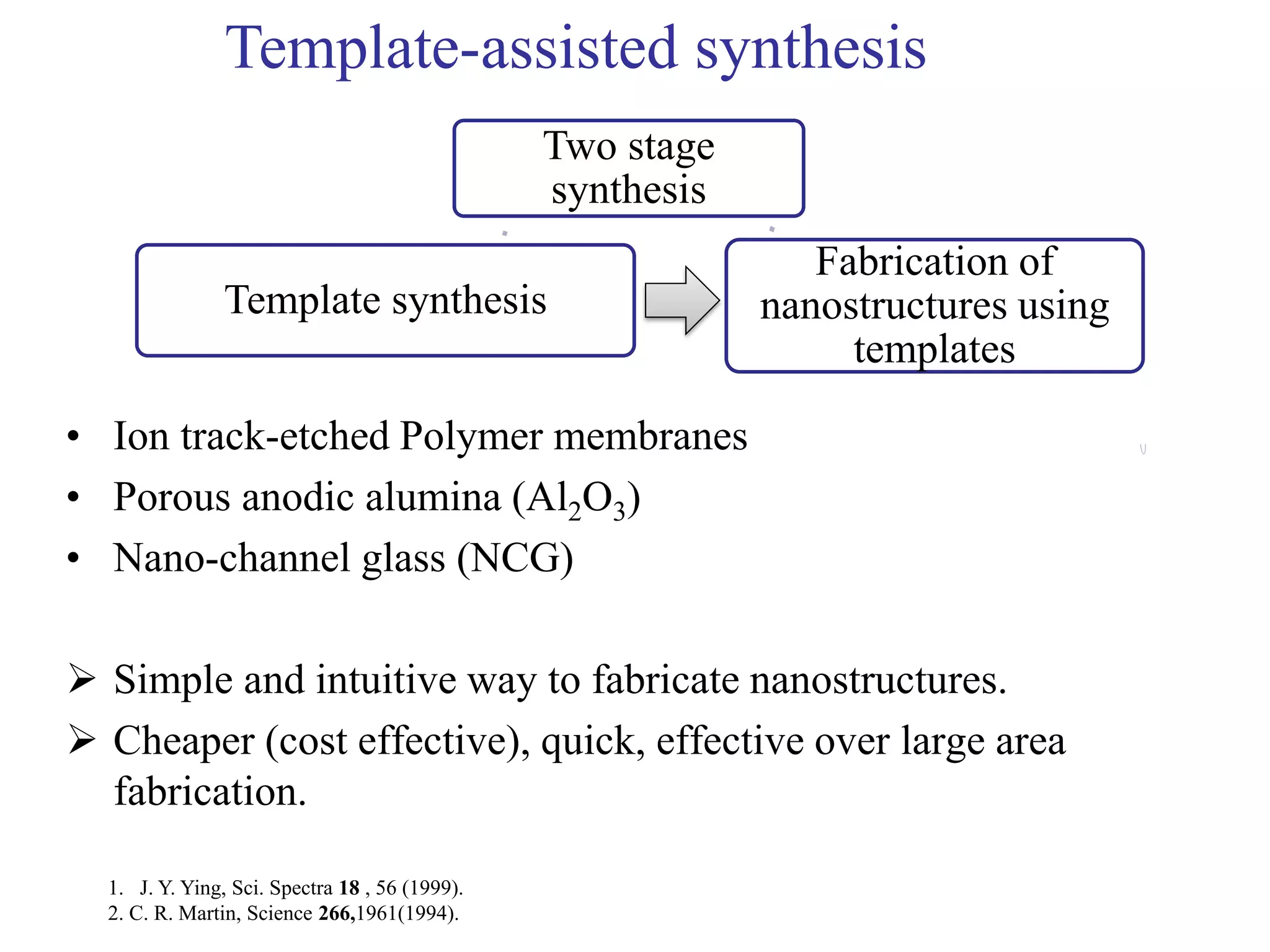
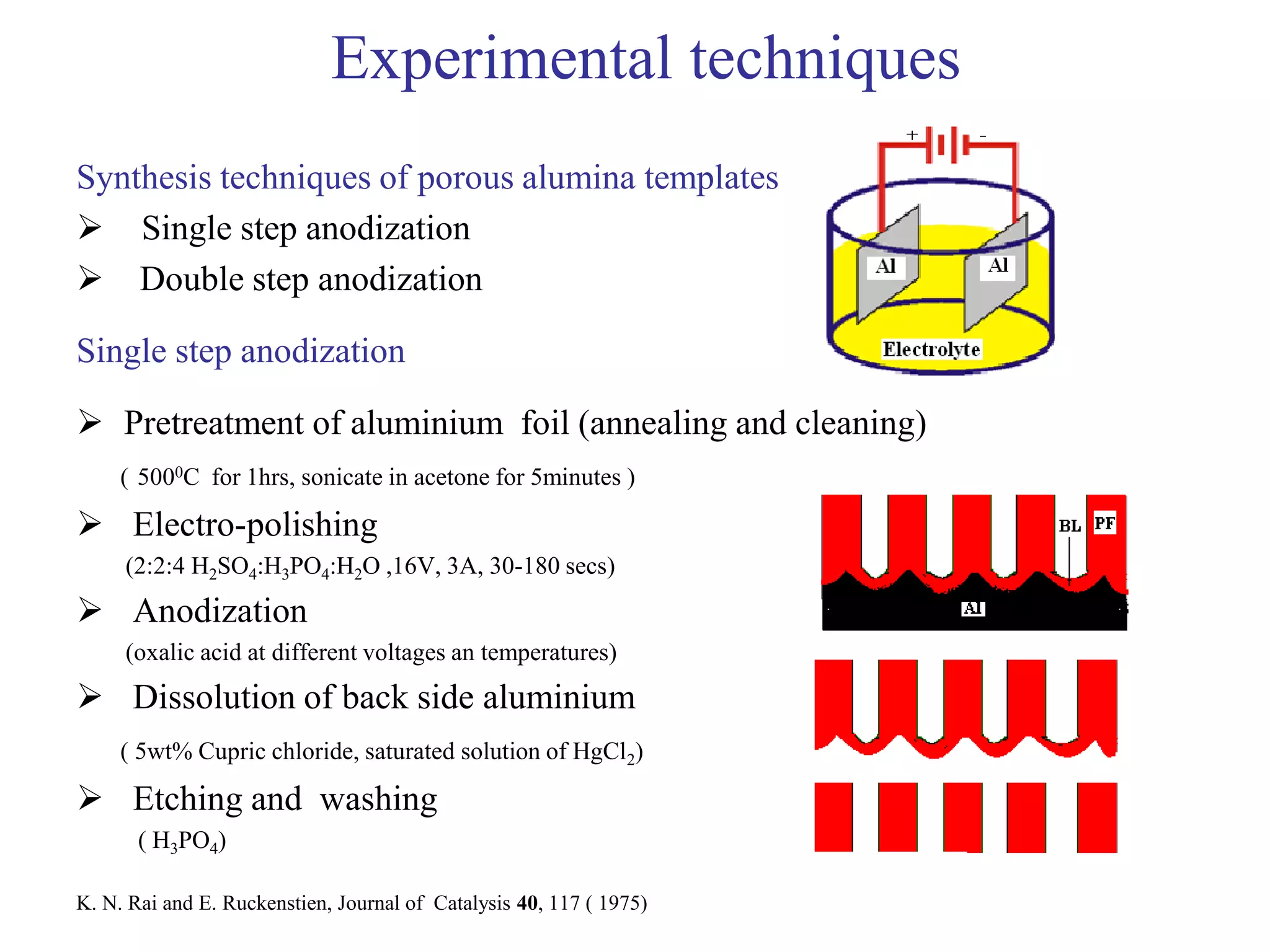
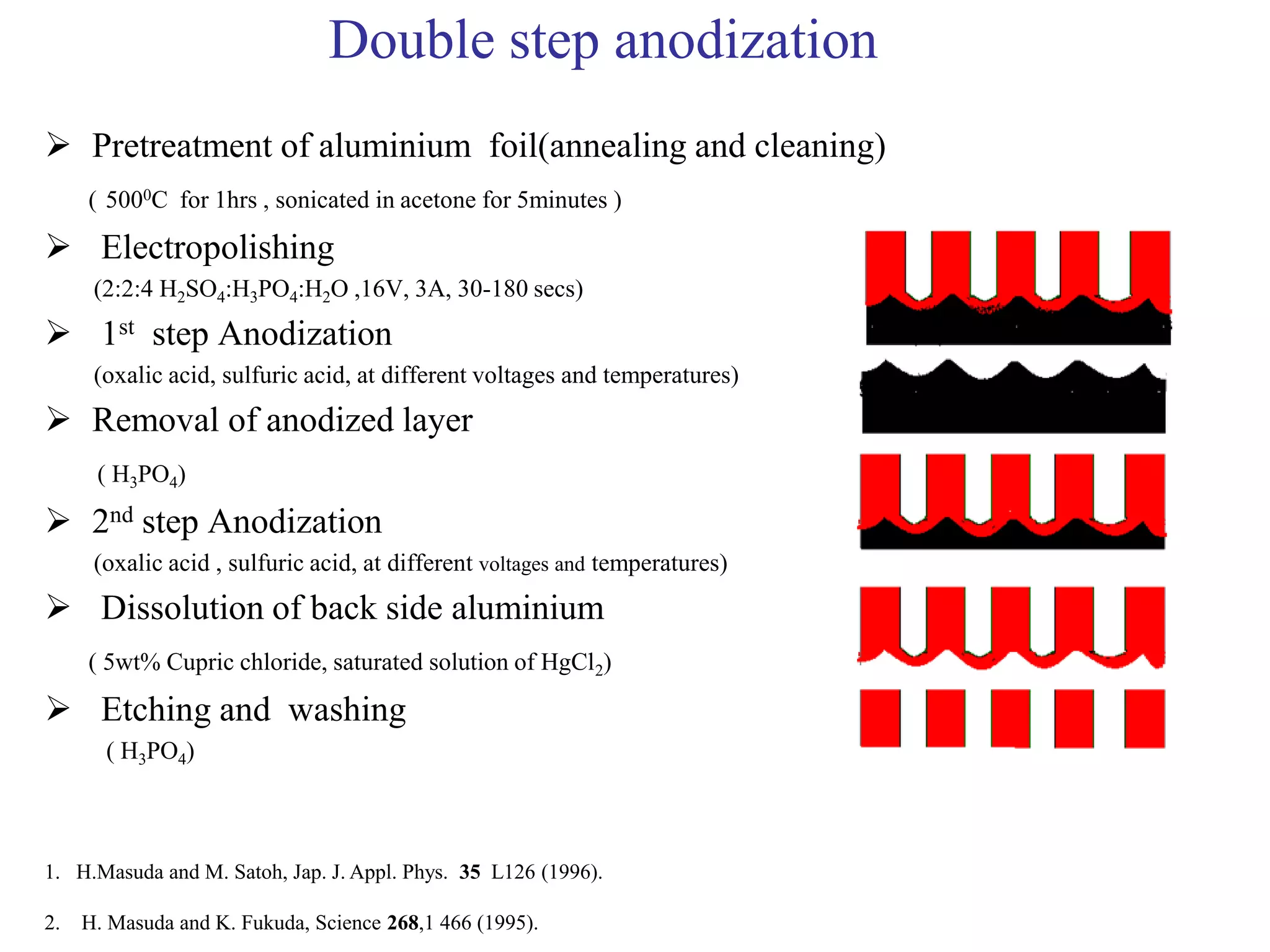
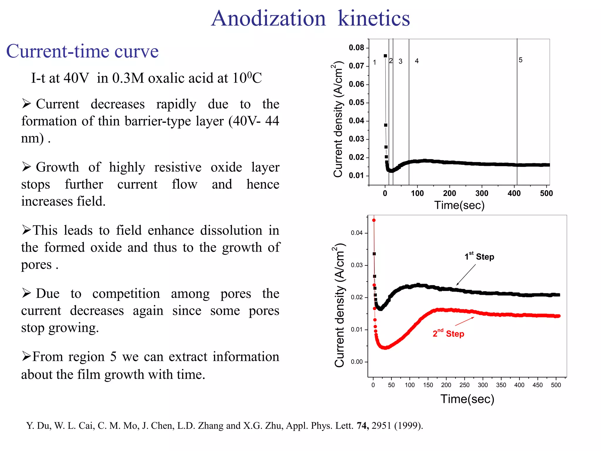
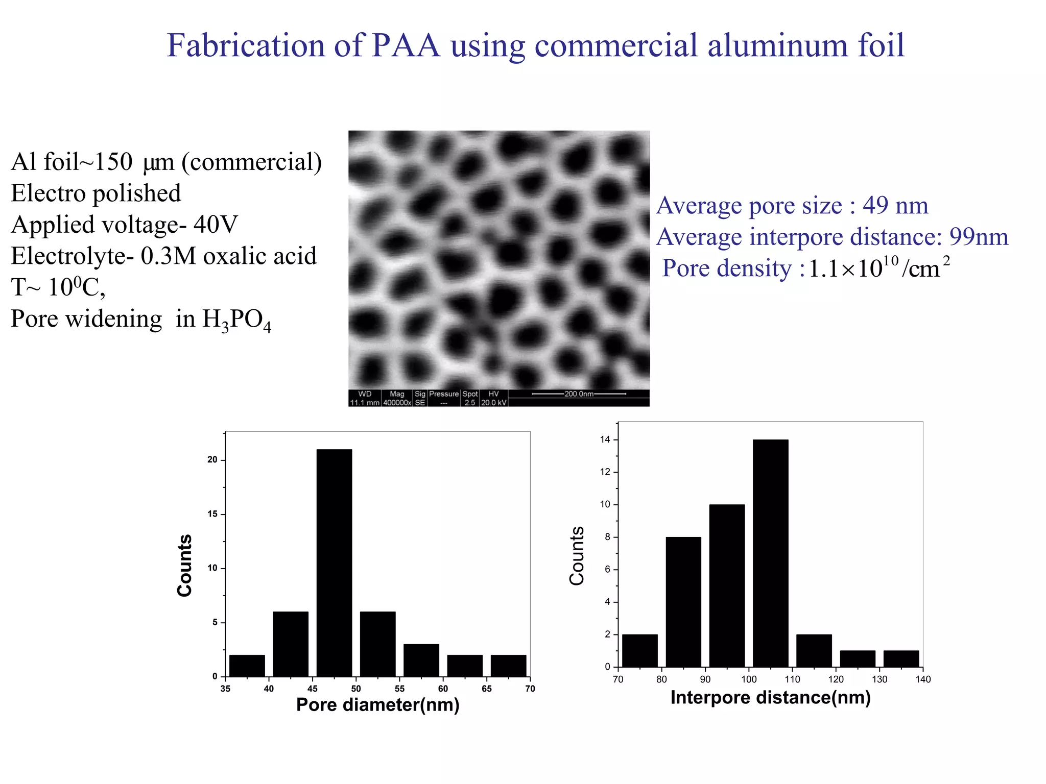
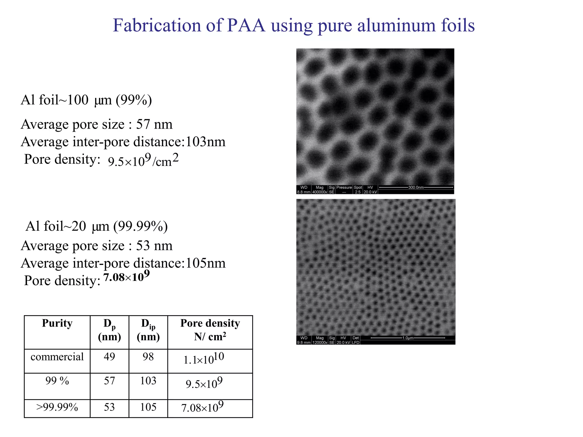
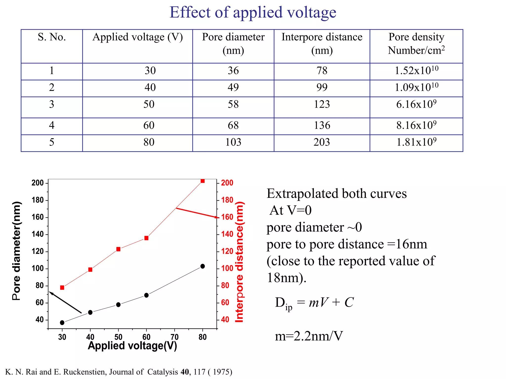
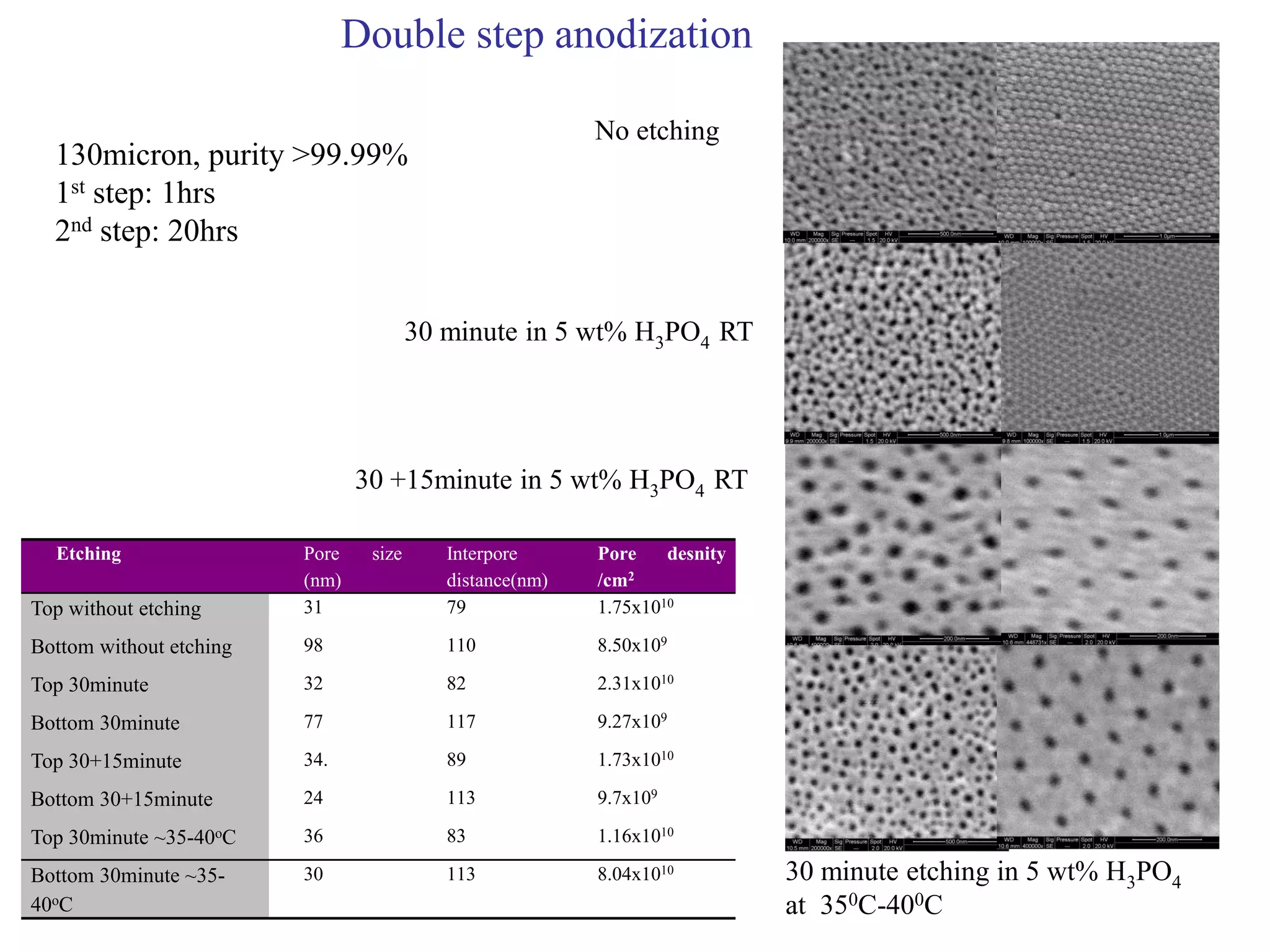
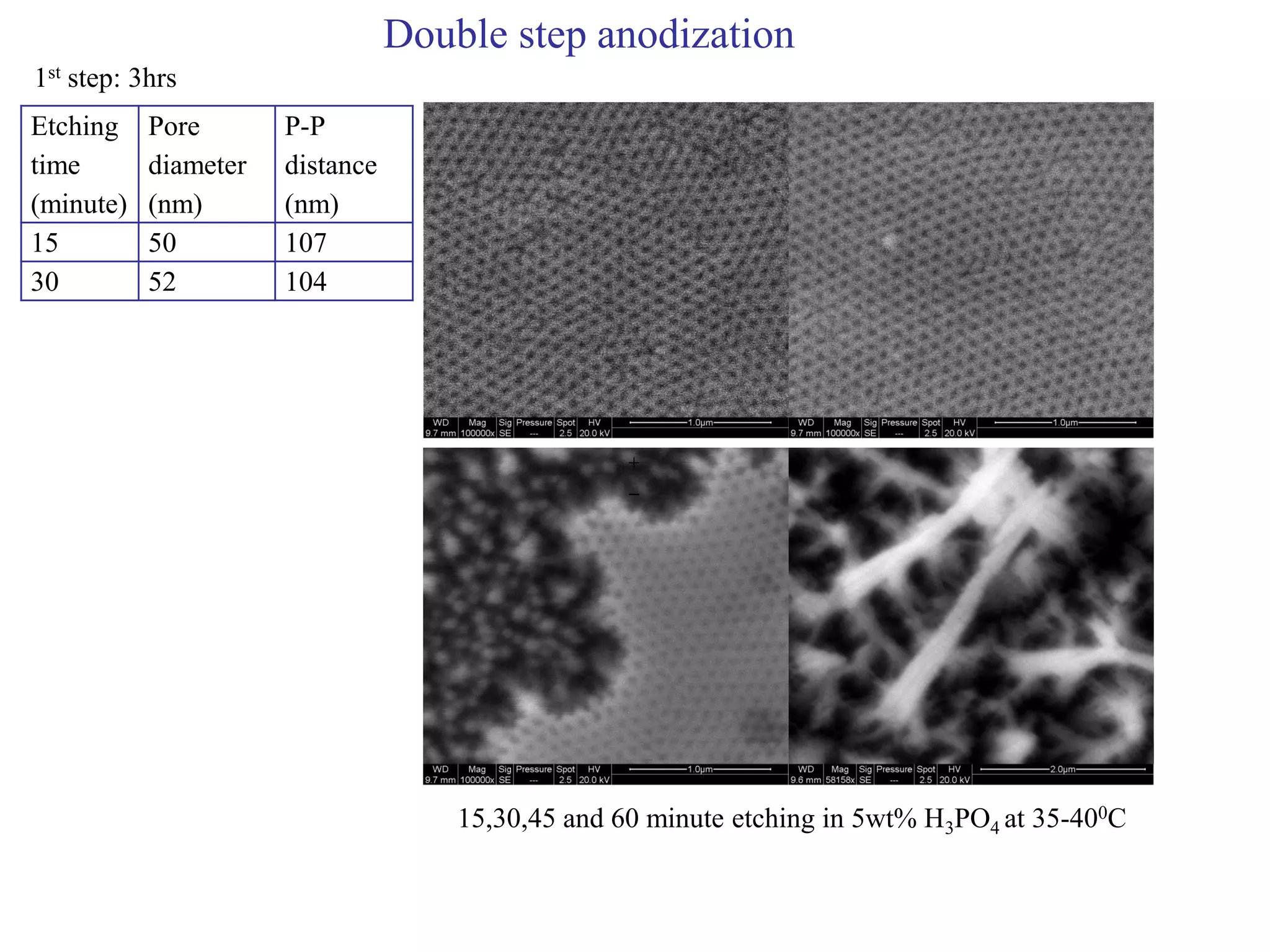
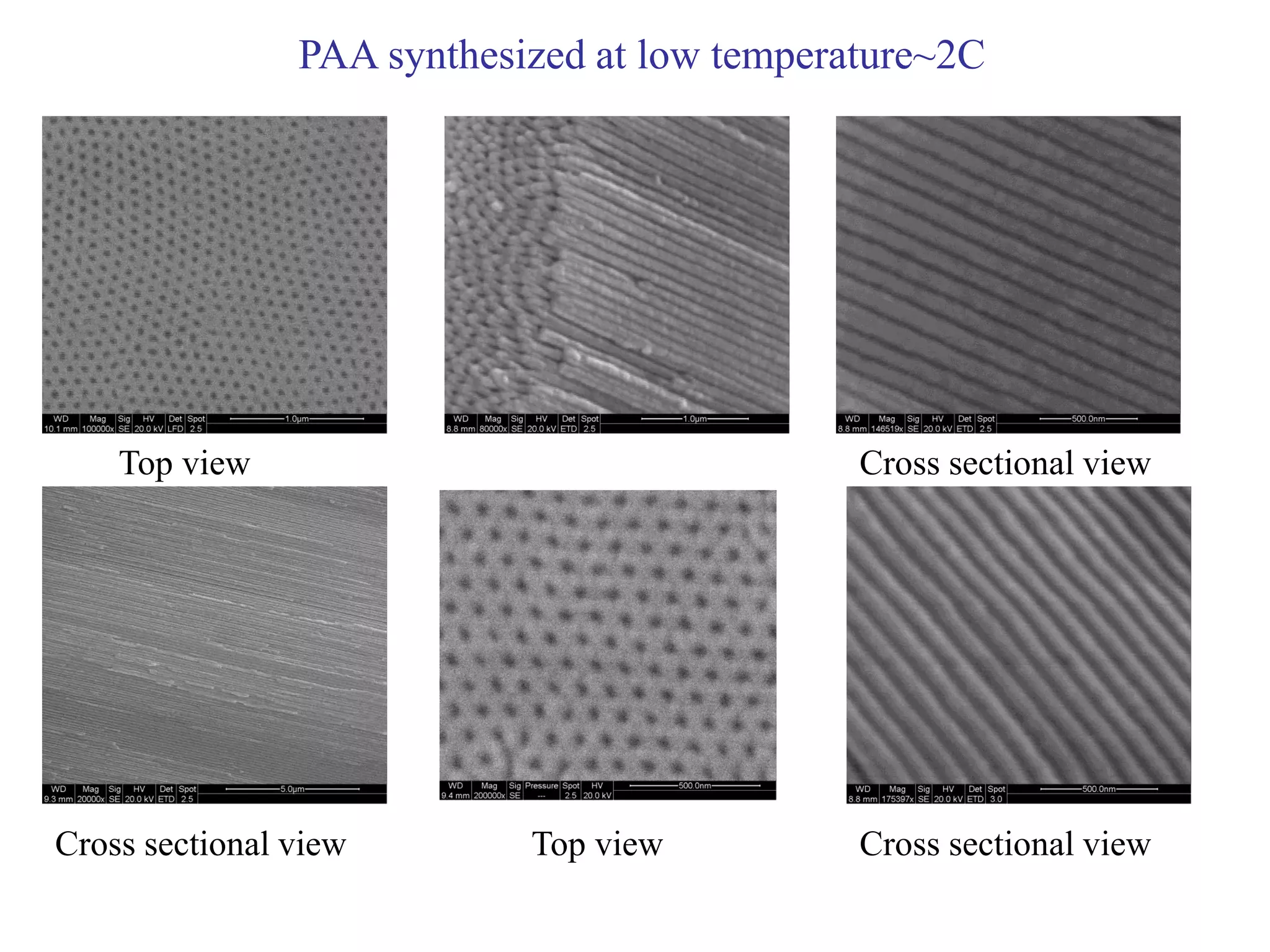
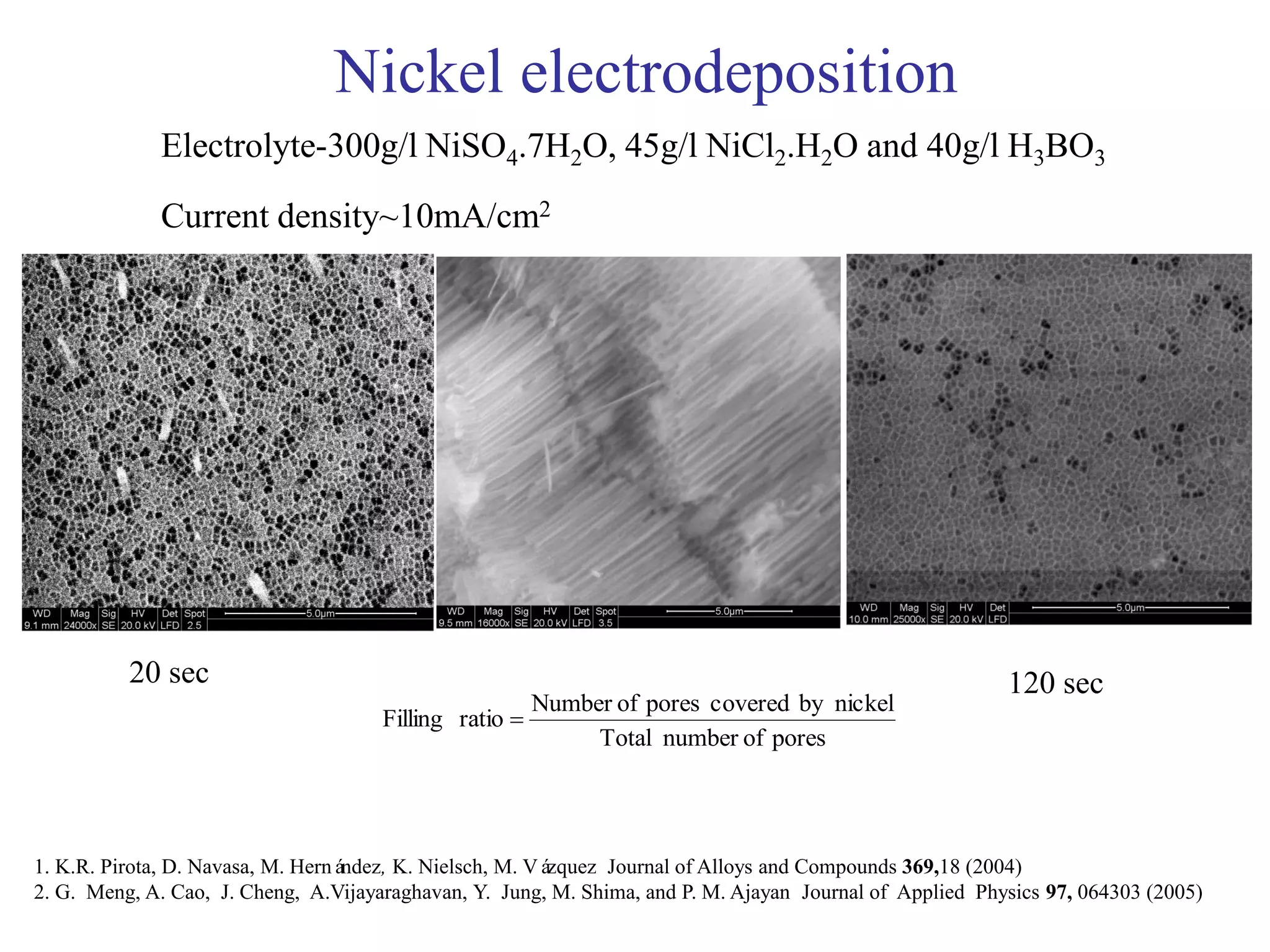
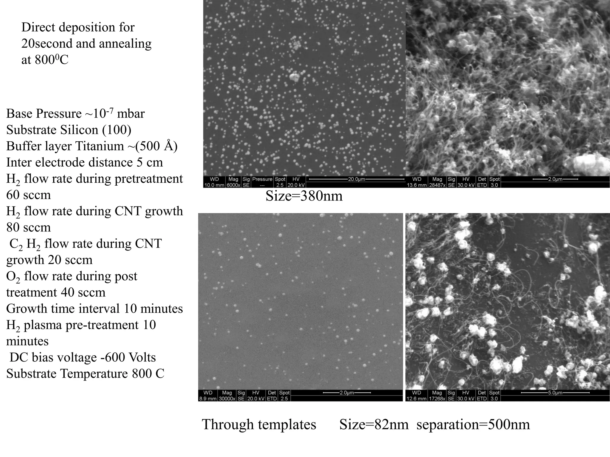
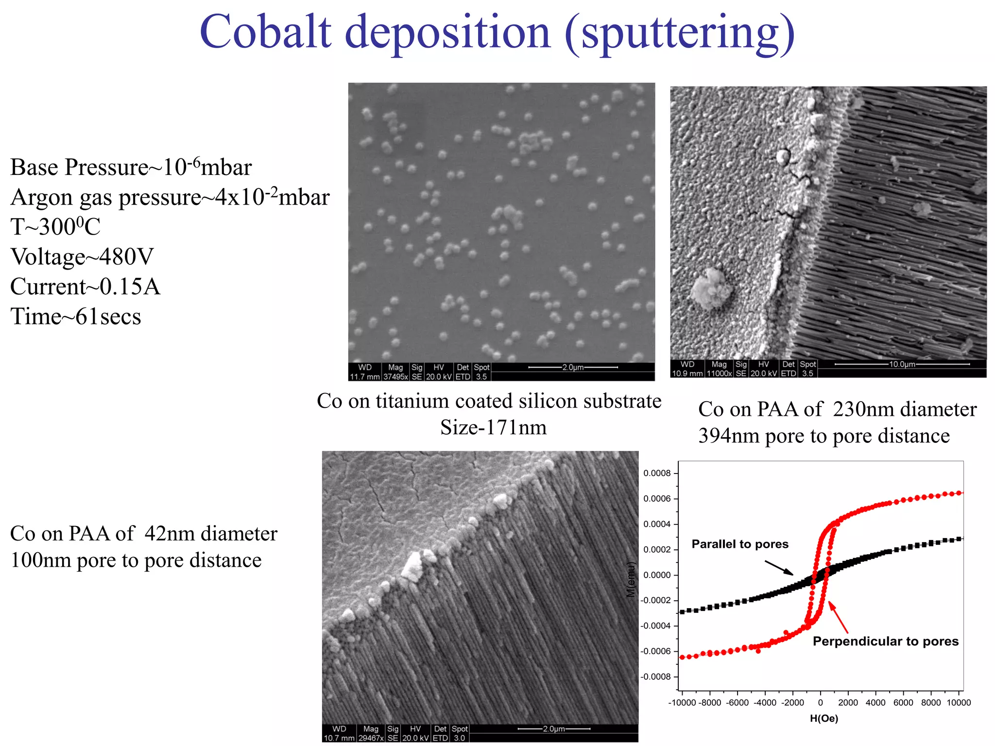
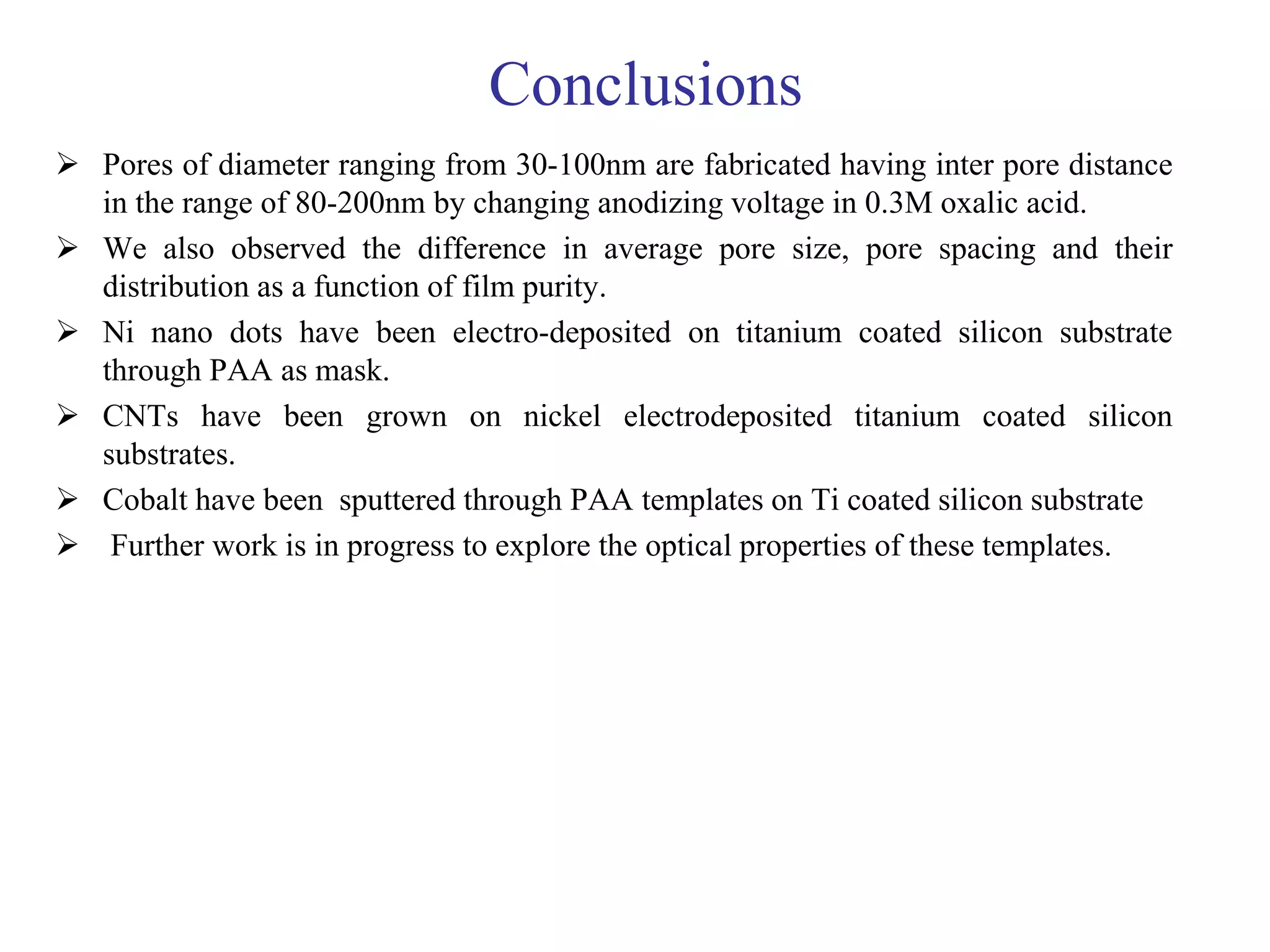
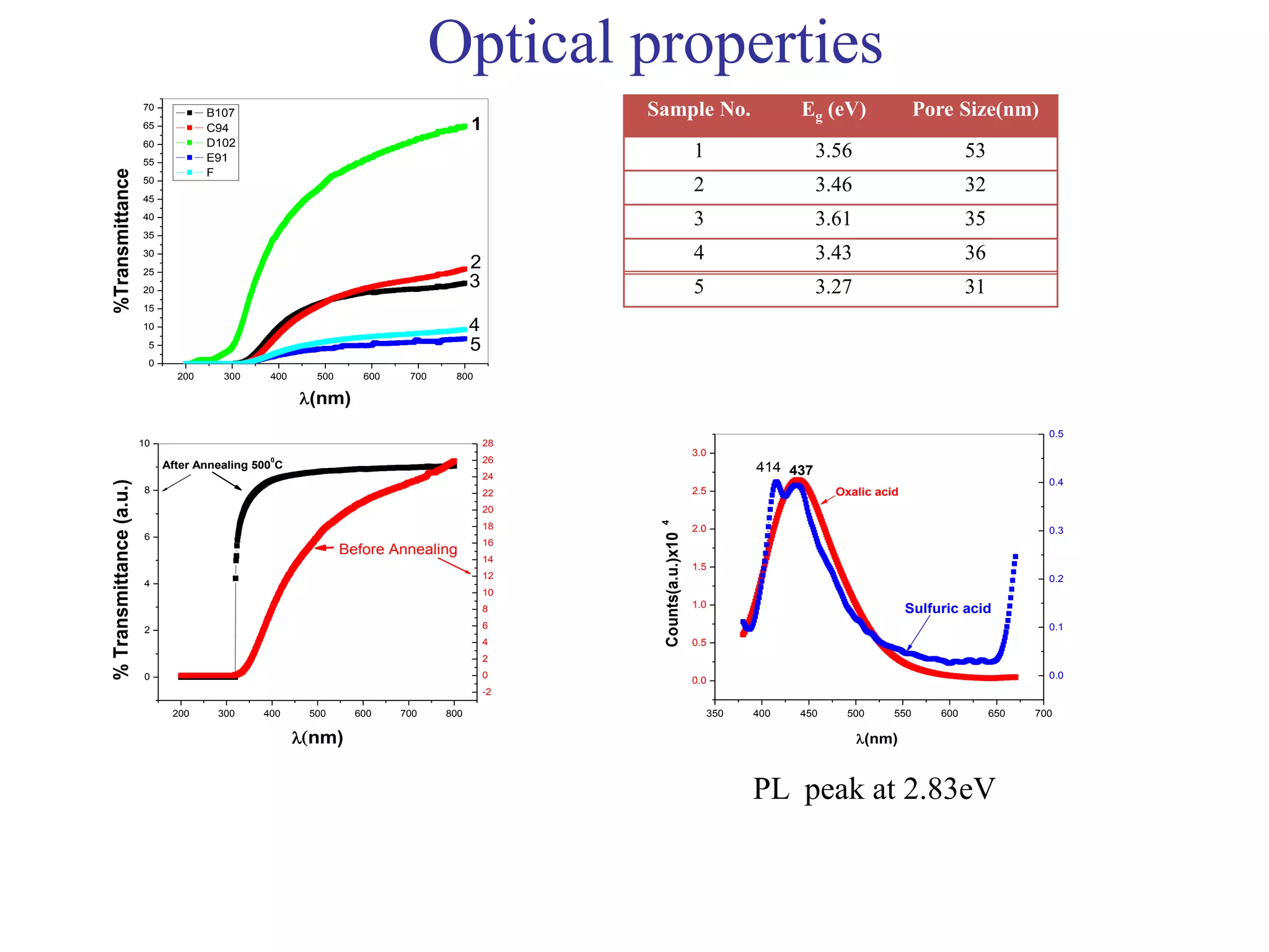
Self-Organized Porous Alumina Templates
and Their Applications
S. K. Yadav
Materials Science Programme,
Indian Institute of Technology Kanpur
,
RAIM08-NIT Hmairpur
Contents
 Introduction
Nanofabrication techniques
Template-assisted synthesis
 Experimental techniques: PAA synthesis
 Anodization kinetics
 PAA templates
 Commercial Aluminium foil
 Pure aluminium foil
 Highly pure aluminium foil
 Nickel deposition
 Cobalt deposition
 Conclusions
 Acknowledgment
Introduction
Nanofabrication techniques
 E-beam and nano-imprint fabrication
 Epitaxy (MBE, MOCVD)
 Scanning probe technique
 Self-assembly and template synthesis
Approach
 Top-Down- Size and distribution can be controlled.
Limitation- Small area fabrication < 100μm x100μm
 Bottom-up- Direct growth of smallest structures : Starting with building
blocks, difficult to control size and locations.
Synthesis of nanostructures by template synthesis technique is combination of
above two: Template by top-down then nanostructures by bottom-up
• Ion track-etched Polymer membranes
• Porous anodic alumina (Al2O3)
• Nano-channel glass (NCG)
 Simple and intuitive way to fabricate nanostructures.
 Cheaper (cost effective), quick, effective over large area
fabrication.
Template-assisted synthesis
Two stage
synthesis
Fabrication of
nanostructures using
templates
Template synthesis
1. J. Y. Ying, Sci. Spectra 18 , 56 (1999).
2. C. R. Martin, Science 266,1961(1994).
Experimental techniques
Synthesis techniques of porous alumina templates
 Single step anodization
 Double step anodization
Single step anodization
 Pretreatment of aluminium foil (annealing and cleaning)
( 5000C for 1hrs, sonicate in acetone for 5minutes )
 Electro-polishing
(2:2:4 H2SO4:H3PO4:H2O ,16V, 3A, 30-180 secs)
 Anodization
(oxalic acid at different voltages an temperatures)
 Dissolution of back side aluminium
( 5wt% Cupric chloride, saturated solution of HgCl2)
 Etching and washing
( H3PO4)
K. N. Rai and E. Ruckenstien, Journal of Catalysis 40, 117 ( 1975)
Double step anodization
 Pretreatment of aluminium foil(annealing and cleaning)
( 5000C for 1hrs , sonicated in acetone for 5minutes )
 Electropolishing
(2:2:4 H2SO4:H3PO4:H2O ,16V, 3A, 30-180 secs)
 1st step Anodization
(oxalic acid, sulfuric acid, at different voltages and temperatures)
 Removal of anodized layer
( H3PO4)
 2nd step Anodization
(oxalic acid , sulfuric acid, at different voltages and temperatures)
 Dissolution of back side aluminium
( 5wt% Cupric chloride, saturated solution of HgCl2)
 Etching and washing
( H3PO4)
1. H.Masuda and M. Satoh, Jap. J. Appl. Phys. 35 L126 (1996).
2. H. Masuda and K. Fukuda, Science 268,1 466 (1995).
Current-time curve
0 100 200 300 400 500
0.01
0.02
0.03
0.04
0.05
0.06
0.07
0.08
Currentdensity(A/cm
2
)
5432
Time(sec)
1
I-t at 40V in 0.3M oxalic acid at 100C
0 50 100 150 200 250 300 350 400 450 500
0.00
0.01
0.02
0.03
0.04
1
st
Step
2
nd
Step
Currentdensity(A/cm
2
)
Time(sec)
 Current decreases rapidly due to the
formation of thin barrier-type layer (40V- 44
nm) .
 Growth of highly resistive oxide layer
stops further current flow and hence
increases field.
This leads to field enhance dissolution in
the formed oxide and thus to the growth of
pores .
 Due to competition among pores the
current decreases again since some pores
stop growing.
From region 5 we can extract information
about the film growth with time.
Anodization kinetics
Y. Du, W. L. Cai, C. M. Mo, J. Chen, L.D. Zhang and X.G. Zhu, Appl. Phys. Lett. 74, 2951 (1999).
Fabrication of PAA using commercial aluminum foil
Average pore size : 49 nm
Average interpore distance: 99nm
Pore density : 210
/cm101.1
Al foil~150 µm (commercial)
Electro polished
Applied voltage- 40V
Electrolyte- 0.3M oxalic acid
T~ 100C,
Pore widening in H3PO4
35 40 45 50 55 60 65 70
0
5
10
15
20
Counts
Pore diameter(nm)
70 80 90 100 110 120 130 140
0
2
4
6
8
10
12
14
Counts
Interpore distance(nm)
Al foil~100 µm (99%)
Average pore size : 57 nm
Average inter-pore distance:103nm
Pore density:
Al foil~20 µm (99.99%)
Average pore size : 53 nm
Average inter-pore distance:105nm
Pore density:
Purity Dp
(nm)
Dip
(nm)
Pore density
N/ cm2
commercial 49 98
99 % 57 103
>99.99% 53 105
10101.1
9109.5
9107.08
2/cm9109.5
9107.08
Fabrication of PAA using pure aluminum foils
Effect of applied voltage
S. No. Applied voltage (V) Pore diameter
(nm)
Interpore distance
(nm)
Pore density
Number/cm2
1 30 36 78 1.52x10¹⁰
2 40 49 99 1.09x10¹⁰
3 50 58 123 6.16x10⁹
4 60 68 136 8.16x10⁹
5 80 103 203 1.81x10⁹
30 40 50 60 70 80
40
60
80
100
120
140
160
180
200
40
60
80
100
120
140
160
180
200
Interporedistance(nm)
Porediameter(nm)
Applied voltage(V)
Extrapolated both curves
At V=0
pore diameter ~0
pore to pore distance =16nm
(close to the reported value of
18nm).
Dip = mV + C
m=2.2nm/V
K. N. Rai and E. Ruckenstien, Journal of Catalysis 40, 117 ( 1975)
Double step anodization
130micron, purity >99.99%
1st step: 1hrs
2nd step: 20hrs
30 minute in 5 wt% H3PO4 RT
No etching
30 +15minute in 5 wt% H3PO4 RT
30 minute etching in 5 wt% H3PO4
at 350C-400C
Etching Pore size
(nm)
Interpore
distance(nm)
Pore desnity
/cm2
Top without etching 31 79 1.75x10¹⁰
Bottom without etching 98 110 8.50x10⁹
Top 30minute 32 82 2.31x10¹⁰
Bottom 30minute 77 117 9.27x10⁹
Top 30+15minute 34. 89 1.73x10¹⁰
Bottom 30+15minute 24 113 9.7x10⁹
Top 30minute ~35-40oC 36 83 1.16x10¹⁰
Bottom 30minute ~35-
40oC
30 113 8.04x10¹⁰
1st step: 3hrs
15,30,45 and 60 minute etching in 5wt% H3PO4 at 35-400C
Etching
time
(minute)
Pore
diameter
(nm)
P-P
distance
(nm)
15 50 107
30 52 104


Double step anodization
PAA synthesized at low temperature~2C
Cross sectional view
Cross sectional viewCross sectional view Top view
Top view
Nickel electrodeposition
Electrolyte-300g/l NiSO4.7H2O, 45g/l NiCl2.H2O and 40g/l H3BO3
Current density~10mA/cm2
20 sec 120 sec
poresofnumberTotal
nickelbycoveredporesofNumber
ratioFilling 
1. K.R. Pirota, D. Navasa, M. Hernández, K. Nielsch, M. Vázquez Journal of Alloys and Compounds 369,18 (2004)
2. G. Meng, A. Cao, J. Cheng, A.Vijayaraghavan, Y. Jung, M. Shima, and P. M. Ajayan Journal of Applied Physics 97, 064303 (2005)
Through templates Size=82nm separation=500nm
Direct deposition for
20second and annealing
at 8000C
Base Pressure ~10-7 mbar
Substrate Silicon (100)
Buffer layer Titanium ~(500 Å)
Inter electrode distance 5 cm
H2 flow rate during pretreatment
60 sccm
H2 flow rate during CNT growth
80 sccm
C2 H2 flow rate during CNT
growth 20 sccm
O2 flow rate during post
treatment 40 sccm
Growth time interval 10 minutes
H2 plasma pre-treatment 10
minutes
DC bias voltage -600 Volts
Substrate Temperature 800 C
Size=380nm
Cobalt deposition (sputtering)
Base Pressure~10-6mbar
Argon gas pressure~4x10⁻²mbar
T~3000C
Voltage~480V
Current~0.15A
Time~61secs
Co on titanium coated silicon substrate
Size-171nm
Co on PAA of 42nm diameter
100nm pore to pore distance
Co on PAA of 230nm diameter
394nm pore to pore distance
-10000 -8000 -6000 -4000 -2000 0 2000 4000 6000 8000 10000
-0.0008
-0.0006
-0.0004
-0.0002
0.0000
0.0002
0.0004
0.0006
0.0008
Perpendicular to pores
Parallel to pores
M(emu)
H(Oe)
Conclusions
 Pores of diameter ranging from 30-100nm are fabricated having inter pore distance
in the range of 80-200nm by changing anodizing voltage in 0.3M oxalic acid.
 We also observed the difference in average pore size, pore spacing and their
distribution as a function of film purity.
 Ni nano dots have been electro-deposited on titanium coated silicon substrate
through PAA as mask.
 CNTs have been grown on nickel electrodeposited titanium coated silicon
substrates.
 Cobalt have been sputtered through PAA templates on Ti coated silicon substrate
 Further work is in progress to explore the optical properties of these templates.
Acknowledgment
• Thanks CSIR for financial support
• Thanks RAIM08
• Thanks Shyam, D. N. Patel, Durgesh and Dibyendu.
30V 50V
60V 80V
Optical properties
200 300 400 500 600 700 800
0
5
10
15
20
25
30
35
40
45
50
55
60
65
70
3
4
5
1
2
%Transmittance
(nm)
B107
C94
D102
E91
F
Sample No. Eg (eV) Pore Size(nm)
1 3.56 53
2 3.46 32
3 3.61 35
4 3.43 36
5 3.27 31
200 300 400 500 600 700 800
0
2
4
6
8
10
-2
0
2
4
6
8
10
12
14
16
18
20
22
24
26
28
%Transmittance(a.u.)
 nm)
Before Annealing
After Annealing 500
0
C
350 400 450 500 550 600 650 700
0.0
0.5
1.0
1.5
2.0
2.5
3.0
0.0
0.1
0.2
0.3
0.4
0.5
Counts(a.u.)x10
4
(nm)
437414
Sulfuric acid
Oxalic acid
PL peak at 2.83eV

Santosh_Kr_Yadav_RAIM08

  • 1.
    Self-Organized Porous AluminaTemplates and Their Applications S. K. Yadav Materials Science Programme, Indian Institute of Technology Kanpur , RAIM08-NIT Hmairpur
  • 2.
    Contents  Introduction Nanofabrication techniques Template-assistedsynthesis  Experimental techniques: PAA synthesis  Anodization kinetics  PAA templates  Commercial Aluminium foil  Pure aluminium foil  Highly pure aluminium foil  Nickel deposition  Cobalt deposition  Conclusions  Acknowledgment
  • 3.
    Introduction Nanofabrication techniques  E-beamand nano-imprint fabrication  Epitaxy (MBE, MOCVD)  Scanning probe technique  Self-assembly and template synthesis Approach  Top-Down- Size and distribution can be controlled. Limitation- Small area fabrication < 100μm x100μm  Bottom-up- Direct growth of smallest structures : Starting with building blocks, difficult to control size and locations. Synthesis of nanostructures by template synthesis technique is combination of above two: Template by top-down then nanostructures by bottom-up
  • 4.
    • Ion track-etchedPolymer membranes • Porous anodic alumina (Al2O3) • Nano-channel glass (NCG)  Simple and intuitive way to fabricate nanostructures.  Cheaper (cost effective), quick, effective over large area fabrication. Template-assisted synthesis Two stage synthesis Fabrication of nanostructures using templates Template synthesis 1. J. Y. Ying, Sci. Spectra 18 , 56 (1999). 2. C. R. Martin, Science 266,1961(1994).
  • 5.
    Experimental techniques Synthesis techniquesof porous alumina templates  Single step anodization  Double step anodization Single step anodization  Pretreatment of aluminium foil (annealing and cleaning) ( 5000C for 1hrs, sonicate in acetone for 5minutes )  Electro-polishing (2:2:4 H2SO4:H3PO4:H2O ,16V, 3A, 30-180 secs)  Anodization (oxalic acid at different voltages an temperatures)  Dissolution of back side aluminium ( 5wt% Cupric chloride, saturated solution of HgCl2)  Etching and washing ( H3PO4) K. N. Rai and E. Ruckenstien, Journal of Catalysis 40, 117 ( 1975)
  • 6.
    Double step anodization Pretreatment of aluminium foil(annealing and cleaning) ( 5000C for 1hrs , sonicated in acetone for 5minutes )  Electropolishing (2:2:4 H2SO4:H3PO4:H2O ,16V, 3A, 30-180 secs)  1st step Anodization (oxalic acid, sulfuric acid, at different voltages and temperatures)  Removal of anodized layer ( H3PO4)  2nd step Anodization (oxalic acid , sulfuric acid, at different voltages and temperatures)  Dissolution of back side aluminium ( 5wt% Cupric chloride, saturated solution of HgCl2)  Etching and washing ( H3PO4) 1. H.Masuda and M. Satoh, Jap. J. Appl. Phys. 35 L126 (1996). 2. H. Masuda and K. Fukuda, Science 268,1 466 (1995).
  • 7.
    Current-time curve 0 100200 300 400 500 0.01 0.02 0.03 0.04 0.05 0.06 0.07 0.08 Currentdensity(A/cm 2 ) 5432 Time(sec) 1 I-t at 40V in 0.3M oxalic acid at 100C 0 50 100 150 200 250 300 350 400 450 500 0.00 0.01 0.02 0.03 0.04 1 st Step 2 nd Step Currentdensity(A/cm 2 ) Time(sec)  Current decreases rapidly due to the formation of thin barrier-type layer (40V- 44 nm) .  Growth of highly resistive oxide layer stops further current flow and hence increases field. This leads to field enhance dissolution in the formed oxide and thus to the growth of pores .  Due to competition among pores the current decreases again since some pores stop growing. From region 5 we can extract information about the film growth with time. Anodization kinetics Y. Du, W. L. Cai, C. M. Mo, J. Chen, L.D. Zhang and X.G. Zhu, Appl. Phys. Lett. 74, 2951 (1999).
  • 8.
    Fabrication of PAAusing commercial aluminum foil Average pore size : 49 nm Average interpore distance: 99nm Pore density : 210 /cm101.1 Al foil~150 µm (commercial) Electro polished Applied voltage- 40V Electrolyte- 0.3M oxalic acid T~ 100C, Pore widening in H3PO4 35 40 45 50 55 60 65 70 0 5 10 15 20 Counts Pore diameter(nm) 70 80 90 100 110 120 130 140 0 2 4 6 8 10 12 14 Counts Interpore distance(nm)
  • 9.
    Al foil~100 µm(99%) Average pore size : 57 nm Average inter-pore distance:103nm Pore density: Al foil~20 µm (99.99%) Average pore size : 53 nm Average inter-pore distance:105nm Pore density: Purity Dp (nm) Dip (nm) Pore density N/ cm2 commercial 49 98 99 % 57 103 >99.99% 53 105 10101.1 9109.5 9107.08 2/cm9109.5 9107.08 Fabrication of PAA using pure aluminum foils
  • 10.
    Effect of appliedvoltage S. No. Applied voltage (V) Pore diameter (nm) Interpore distance (nm) Pore density Number/cm2 1 30 36 78 1.52x10¹⁰ 2 40 49 99 1.09x10¹⁰ 3 50 58 123 6.16x10⁹ 4 60 68 136 8.16x10⁹ 5 80 103 203 1.81x10⁹ 30 40 50 60 70 80 40 60 80 100 120 140 160 180 200 40 60 80 100 120 140 160 180 200 Interporedistance(nm) Porediameter(nm) Applied voltage(V) Extrapolated both curves At V=0 pore diameter ~0 pore to pore distance =16nm (close to the reported value of 18nm). Dip = mV + C m=2.2nm/V K. N. Rai and E. Ruckenstien, Journal of Catalysis 40, 117 ( 1975)
  • 11.
    Double step anodization 130micron,purity >99.99% 1st step: 1hrs 2nd step: 20hrs 30 minute in 5 wt% H3PO4 RT No etching 30 +15minute in 5 wt% H3PO4 RT 30 minute etching in 5 wt% H3PO4 at 350C-400C Etching Pore size (nm) Interpore distance(nm) Pore desnity /cm2 Top without etching 31 79 1.75x10¹⁰ Bottom without etching 98 110 8.50x10⁹ Top 30minute 32 82 2.31x10¹⁰ Bottom 30minute 77 117 9.27x10⁹ Top 30+15minute 34. 89 1.73x10¹⁰ Bottom 30+15minute 24 113 9.7x10⁹ Top 30minute ~35-40oC 36 83 1.16x10¹⁰ Bottom 30minute ~35- 40oC 30 113 8.04x10¹⁰
  • 12.
    1st step: 3hrs 15,30,45and 60 minute etching in 5wt% H3PO4 at 35-400C Etching time (minute) Pore diameter (nm) P-P distance (nm) 15 50 107 30 52 104   Double step anodization
  • 13.
    PAA synthesized atlow temperature~2C Cross sectional view Cross sectional viewCross sectional view Top view Top view
  • 14.
    Nickel electrodeposition Electrolyte-300g/l NiSO4.7H2O,45g/l NiCl2.H2O and 40g/l H3BO3 Current density~10mA/cm2 20 sec 120 sec poresofnumberTotal nickelbycoveredporesofNumber ratioFilling  1. K.R. Pirota, D. Navasa, M. Hernández, K. Nielsch, M. Vázquez Journal of Alloys and Compounds 369,18 (2004) 2. G. Meng, A. Cao, J. Cheng, A.Vijayaraghavan, Y. Jung, M. Shima, and P. M. Ajayan Journal of Applied Physics 97, 064303 (2005)
  • 15.
    Through templates Size=82nmseparation=500nm Direct deposition for 20second and annealing at 8000C Base Pressure ~10-7 mbar Substrate Silicon (100) Buffer layer Titanium ~(500 Å) Inter electrode distance 5 cm H2 flow rate during pretreatment 60 sccm H2 flow rate during CNT growth 80 sccm C2 H2 flow rate during CNT growth 20 sccm O2 flow rate during post treatment 40 sccm Growth time interval 10 minutes H2 plasma pre-treatment 10 minutes DC bias voltage -600 Volts Substrate Temperature 800 C Size=380nm
  • 16.
    Cobalt deposition (sputtering) BasePressure~10-6mbar Argon gas pressure~4x10⁻²mbar T~3000C Voltage~480V Current~0.15A Time~61secs Co on titanium coated silicon substrate Size-171nm Co on PAA of 42nm diameter 100nm pore to pore distance Co on PAA of 230nm diameter 394nm pore to pore distance -10000 -8000 -6000 -4000 -2000 0 2000 4000 6000 8000 10000 -0.0008 -0.0006 -0.0004 -0.0002 0.0000 0.0002 0.0004 0.0006 0.0008 Perpendicular to pores Parallel to pores M(emu) H(Oe)
  • 17.
    Conclusions  Pores ofdiameter ranging from 30-100nm are fabricated having inter pore distance in the range of 80-200nm by changing anodizing voltage in 0.3M oxalic acid.  We also observed the difference in average pore size, pore spacing and their distribution as a function of film purity.  Ni nano dots have been electro-deposited on titanium coated silicon substrate through PAA as mask.  CNTs have been grown on nickel electrodeposited titanium coated silicon substrates.  Cobalt have been sputtered through PAA templates on Ti coated silicon substrate  Further work is in progress to explore the optical properties of these templates.
  • 18.
    Acknowledgment • Thanks CSIRfor financial support • Thanks RAIM08 • Thanks Shyam, D. N. Patel, Durgesh and Dibyendu.
  • 19.
  • 20.
    Optical properties 200 300400 500 600 700 800 0 5 10 15 20 25 30 35 40 45 50 55 60 65 70 3 4 5 1 2 %Transmittance (nm) B107 C94 D102 E91 F Sample No. Eg (eV) Pore Size(nm) 1 3.56 53 2 3.46 32 3 3.61 35 4 3.43 36 5 3.27 31 200 300 400 500 600 700 800 0 2 4 6 8 10 -2 0 2 4 6 8 10 12 14 16 18 20 22 24 26 28 %Transmittance(a.u.)  nm) Before Annealing After Annealing 500 0 C 350 400 450 500 550 600 650 700 0.0 0.5 1.0 1.5 2.0 2.5 3.0 0.0 0.1 0.2 0.3 0.4 0.5 Counts(a.u.)x10 4 (nm) 437414 Sulfuric acid Oxalic acid PL peak at 2.83eV