Download to read offline
![Microsc. Microanal. Microstruct. 8
(1997)
355-368
DECEMBER
1997,
PAGE
355
Fabrication of Nano-Tips by Carbon Contamination in a Scanning
Electron Microscope for Use in Scanning Probe Microscopy and
Field Emission
Massimo
Antognozzi,
Andrea Sentimenti and
INFM and Centre of Electron
46, 40126 Bologna,
via Irnerio
Ugo Valdrè
Microscopy, Department of Physics of the University,
Italy
(Received August 29, 1997; accepted
December 1,
1997)
PACS.61.16.-d - Electron, ion, and scanning probe microscopy
PACS.79.70.+q -
Field
emission, ionization, evaporation, and desorption
Abstract. 2014 Results are reported on a systematic study addressed to an effective fabrication
of nano-tips by means of carbon contamination in a scanning electron microscope. Nano-tips
with angular aperture of 10°, apical radius of about 5 nm,1 03BCm long can be efficiently produced
by our method in less than 60 s of electron beam exposure; it involves, in particular, successive
focusing during tip growth and the use of a carbon block as a source of contaminant. These tips
have been used as high aspect ratio and low capillary force probes in atomic force microscopy,
and as nano-sized field emitters for electron guns.
1. Introduction
a wide interest in the fabrication of nano-sized tips. At least three major
concerned with their applications: (i) Scanning Probe Microscopy (SPM) [1], (ii)
field emission [2,3] and (iii) field emitter displays [4]. Here we deal specifically with the first
two cases only; however case (iii) will benefit from progress in field (ii).
Case (i) requires probes with the highest possible aspect ratio (i. e., the smallest tip angular
aperture), mechanical strength and the smallest apical radius in order to profile irregular
surfaces with steep slants and to attain high resolution. An additional requirement may be the
electrical conductivity when the probes are to be used in scanning tunneling microscopy and
electric force microscopy.
Case (ii) demands sharp and electrically conducting emitters, in order to get the highest
possible current densities and coherence, with the lowest extraction voltage, for use in electron
guns applied in various types of microscopy and devices.
Usually, probes are made out of metals (e.g., W, Pt, Pt/Ir), semiconductors (Si) or insulators (Si3N4); the latters are sometimes coated with a conducting layer (e.g., Au, Pd, Al)
or a magnetic layer (Ni, Co) depending on the application. Emitters are made of metals or
semiconductors. Here we deal with both probe and emitter tips, fabricated by carbon contamination in a Scanning Electron Microscope (SEM). Whereas this method has been pursued
in several places as far as probes are concerned, nothing has been reported to our knowledge
There is
nowadays
areas are
Oc
EDP Sciences 1998
Article available at http://mmm.edpsciences.org or http://dx.doi.org/10.1051/mmm:1997127
,](https://image.slidesharecdn.com/microscopymicroanalysismicrostructurestheeuropeanphysicaljournalappliedphysicsnanotechnologysentimen-131230173200-phpapp01/75/Microscopy-microanalysis-microstructures_the-european-physical-journal_applied-physics_nanotechnology_sentimenti-1-2048.jpg)
![356
in the case of field emitters. However, the properties of field emitters made of carbon in the
form of nanotubes and diamond chips have been investigated, and the results obtained are
very interesting [4-6]. This paper reports first on the deliberate enhancement of carbon contamination in an SEM, then on an optimized method for the fabrication of carbon nano-tips;
examples of their applications as probes and field emitters are finally presented.
2. Carbon Contamination
Carbon contamination has been studied extensively in electron and ion microscopy with the aim
ideally eliminate it. Very little work has been done so far on the opposite problem
of increasing the contamination selectively, efficiently and in a simple way; such previous work
concerns the production of high aspect ratio probes at the top of cantilevers for application
in scanning probe microscopy by using the electron beam of a SEM. The inconsistent results
we obtained by following empirical recipes suggested by various authors (i.e., use of several
contaminants, such as paraffin oils or blocks), prompted us to tackle the problem afresh.
The following parameters affecting the growth of carbon contamination tips were taken into
account and their effects systematically investigated.
to reduce and
1. SEM
accelerating voltage,
2. beam current, measured with
3. beam
diameter,
4. beam
stability, focus
5.
1
specimen
and
Faraday
eucentric
cup,
level, and corresponding
density,
astigmatism,
material,
coating before carbon-growth for non-conductive specimens.
The pressure in the specimen chamber during the
10-4 Torr and the hydrocarbon partial pressure
x
mass
current
specimen material, shape and clamping,
6. stub
7.
at
a
spectrometer
investigations ranged from 5 x 10⁻⁵ to
about 10-6 Torr, measured with a
was
[7].
The assessment of the tips geometry after their growth was usually made by SEM observations with the tip placed at 90° with respect to the beam; in some cases the observations were
performed in a Transmission Electron Microscope (TEM).
The results are reported below.
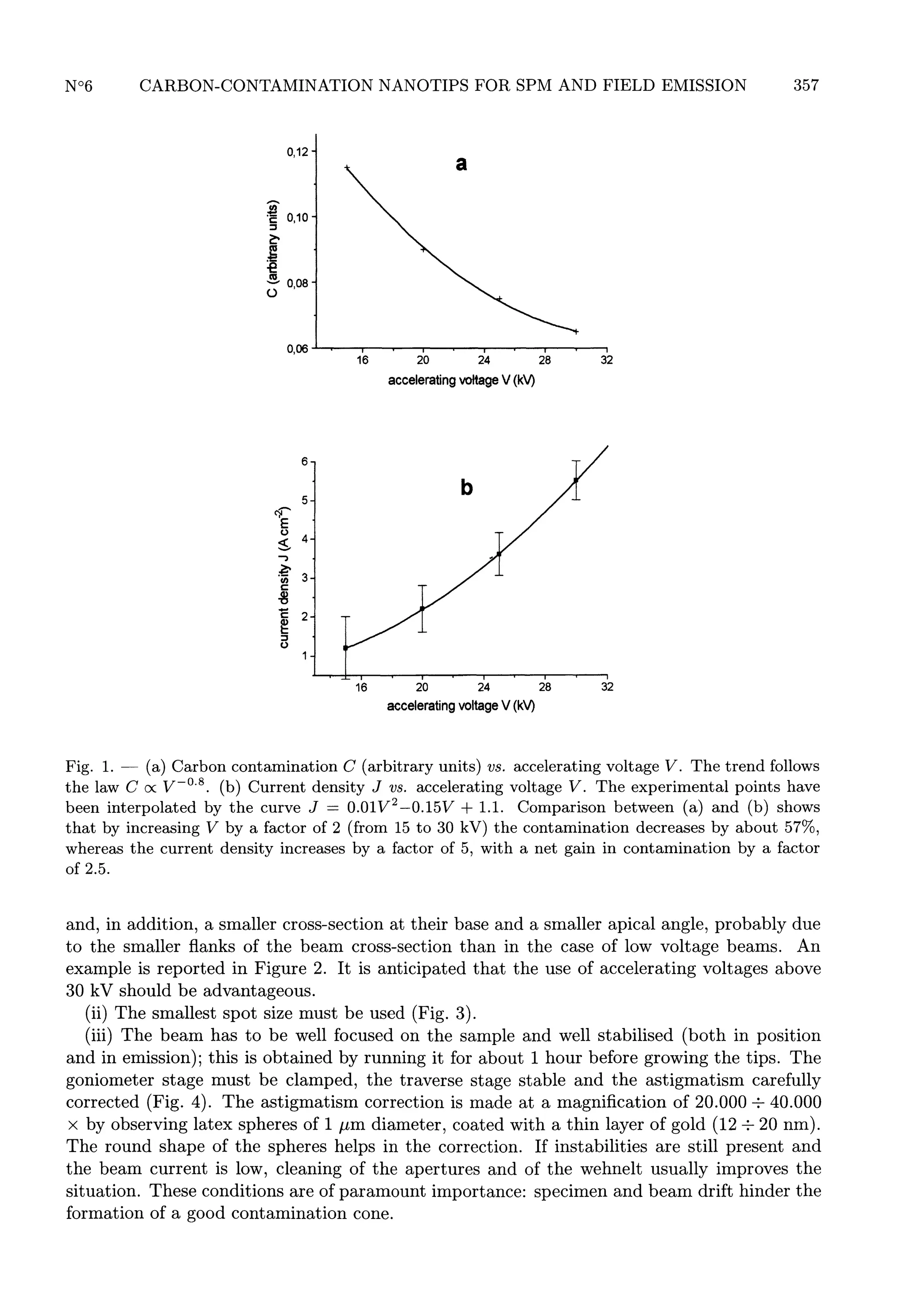
(i) The best accelerating voltage is 30 kV (highest value provided by our instrument, a Philips
SEM 515); the beam current at the specimen level ranged from about 10-12 to 10-13 A and
the corresponding nominal spot sizes were 20 nm and 5 nm (the emission current, read from
the microscope meter, was between 100 and 200 03BCA).
Since it is well known that the contamination rate C increases on decreasing the accelerating
voltage V (C is proportional to V-0-8, Fig. la) [8,9] and is proportional to the current density
J at specimen level, one would expect the best results are obtained at low voltages. However,
the gain in contamination at low voltage does not balance the contamination reduction due to
the decrease of current density connected with the voltage change (Fig. lb) [8,9]. In fact, the
contamination decreases by a factor of about 2.5 by lowering the voltage from 30 to 15 kV.
Tips grown at the highest voltage show better features than those produced at low voltages,
for the same values of the remaining free parameters: they have, of course, a greater height](https://image.slidesharecdn.com/microscopymicroanalysismicrostructurestheeuropeanphysicaljournalappliedphysicsnanotechnologysentimen-131230173200-phpapp01/75/Microscopy-microanalysis-microstructures_the-european-physical-journal_applied-physics_nanotechnology_sentimenti-2-2048.jpg)
![358
SEM secondary electron image taken at 30 kV of two carbon tips grown on a tungsten
surface showing a large difference of geometry and size. (Right side tip) Growth conditions: 15 kV,
60 s, spot size 5 nm, current density 1.1 A cm-2.(Left side tip) Growth conditions: 30 kV, 60 s, spot
size 5 nm, current density 5.6 A cm-2.
Fig.
2.
-
not seem to influence the contamination growth,
tested (Tungsten in the form of wires, plates and microscope
filaments, Tantalum edges, Gold and Palladium films) as long as the specimen is an electrical
conductor and clean. In the case of Si and Si3N4 cantilevers, effective C-contamination growth
is obtained by first coating the substrate with a metal layer (about 20 nm thick of Au or
Pd) to avoid charging up. The carbon growth is more regular on a Pd than on a Au coating
film, owing to the finest size of the Pd clusters. If the above specified conditions are not well
set, contamination rate is low, even with the microscope in standard order; after 10 min of
irradiation only thin (20 2013 80 nm) slightly bulging contamination spots of 50 2013 80 nm diameter
were obtained.
(iv)
The
specimen material and shape do
at least for the
types which
were
(v) Whether the specimen is mechanically clamped or glued with silver dag is irrelevant. On
the contrary, the use of a carbon stub (with the specimen mechanically held), improves the
contamination growth and the reproducibility of the results. Alternatively, simply and cheaply,
use can be made of standard Al stubs to support the specimen and by placing in its vicinity a
small carbon block (N 50 mm3). The effectiveness of the C-block depends on both its surface
and its distance from the specimen region where the C-growth has to take place. The growth
rate is 120132 03BCm per minute. The adsorption properties of carbon have been known and exploited
for long time. In the present situation it is believed that under vacuum the carbon block
releases the contaminants previously adsorbed, thus creating a high concentration of carbon
compounds in the proximity of the specimen, which favours the contamination growth [10].
The contamination effect is also well noticeable when a large C-block (surface 50 cm2) is placed
inside the specimen chamber ( e.g., in a corner).](https://image.slidesharecdn.com/microscopymicroanalysismicrostructurestheeuropeanphysicaljournalappliedphysicsnanotechnologysentimen-131230173200-phpapp01/75/Microscopy-microanalysis-microstructures_the-european-physical-journal_applied-physics_nanotechnology_sentimenti-4-2048.jpg)
![359
SEM secondary electron image of a tip grown with a 5 nm beam diameter (left), and of the
Fig. 3.
contamination spot (right) which was produced during an attempt to grow a carbon tip with a large
electron beam diameter (100 nm).
-
(vi) Charging up effects constitute a serious problem when using high accelerating voltages,
since they affect the stability of the electron beam and give rise to drift. The coating of
the substrate with a metal (e.g., gold) overcomes this problem. We also found that coating
obtained by evaporation provides more reproducible results than sputtering.
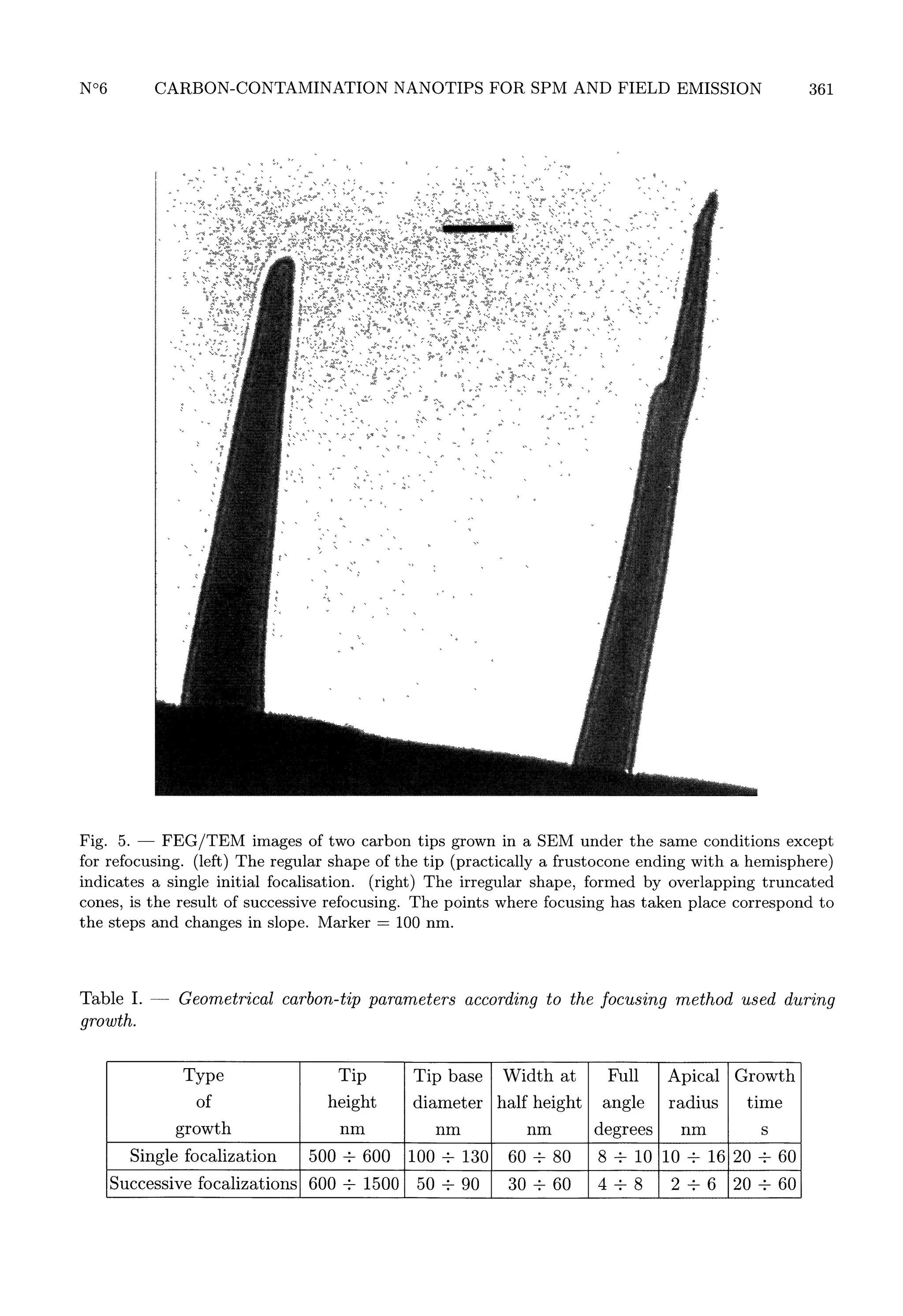
3.
Carbon-Tip
Growth
practical procedure developed to fabricate conically shaped C-tip with small full aperture
angle « 10° ) and a small apical radius « 5 nm) is as follows.
First of all the electron beam, set at the smallest spot, is checked to be spatially and intensity stable (time required usually 1 h) and the astigmatism corrected with the help of latex
spheres. The specimen on which the C-tips have to be grown is then inserted in the SEM. The
The
electron beam is focused over an area where small details are present (observation made at
80.000 2013 160.000 x ) near to the region where the tip has to be grown. Then the beam is
stopped on the latter region. As soon as contamination is formed, astigmatism correction
is again performed by observing the contamination spot. Good focusing, high stability and
careful astigmatism correction are essential operations in order to achieve high quality tips;
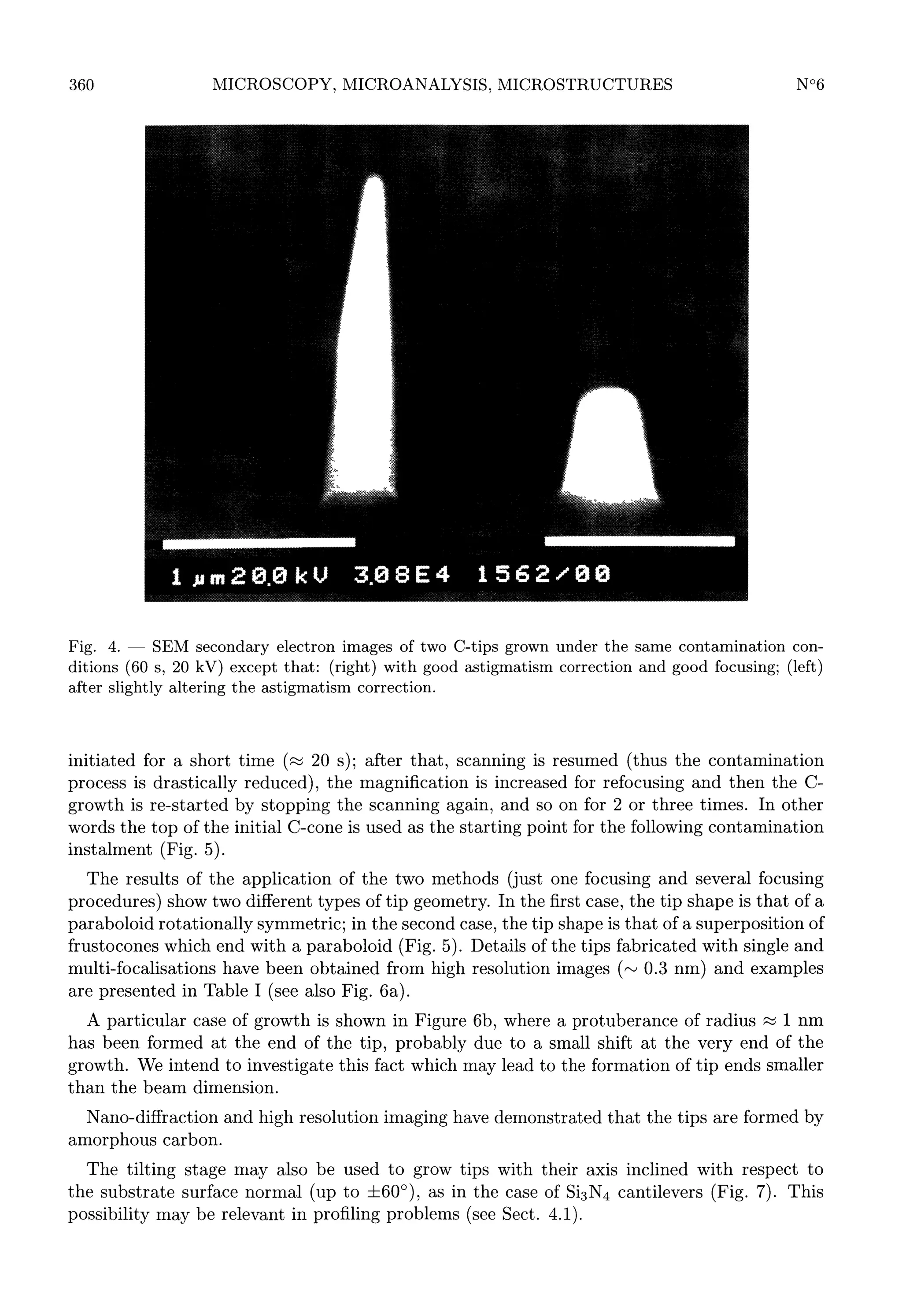
otherwise the regular shape, the sharpness and even the growth rate are jeopardised (Fig. 4).
During the growth of contamination, the Secondary Electron (SE) signal (observed in the
y-monitor) increases because of topographic (edge) effects [11] ; it increases until the tip has
reached its maximum aspect ratio. The beam is then scanned and the geometrical quality of
the tip assessed visually by tilting the specimen stage by 90° with respect to the electron beam.
The finest results are, however, obtained by a focusing sequence: the beam is first scanned
for selecting the region of growth and for focusing, then scanning is stopped and C-growth](https://image.slidesharecdn.com/microscopymicroanalysismicrostructurestheeuropeanphysicaljournalappliedphysicsnanotechnologysentimen-131230173200-phpapp01/75/Microscopy-microanalysis-microstructures_the-european-physical-journal_applied-physics_nanotechnology_sentimenti-5-2048.jpg)
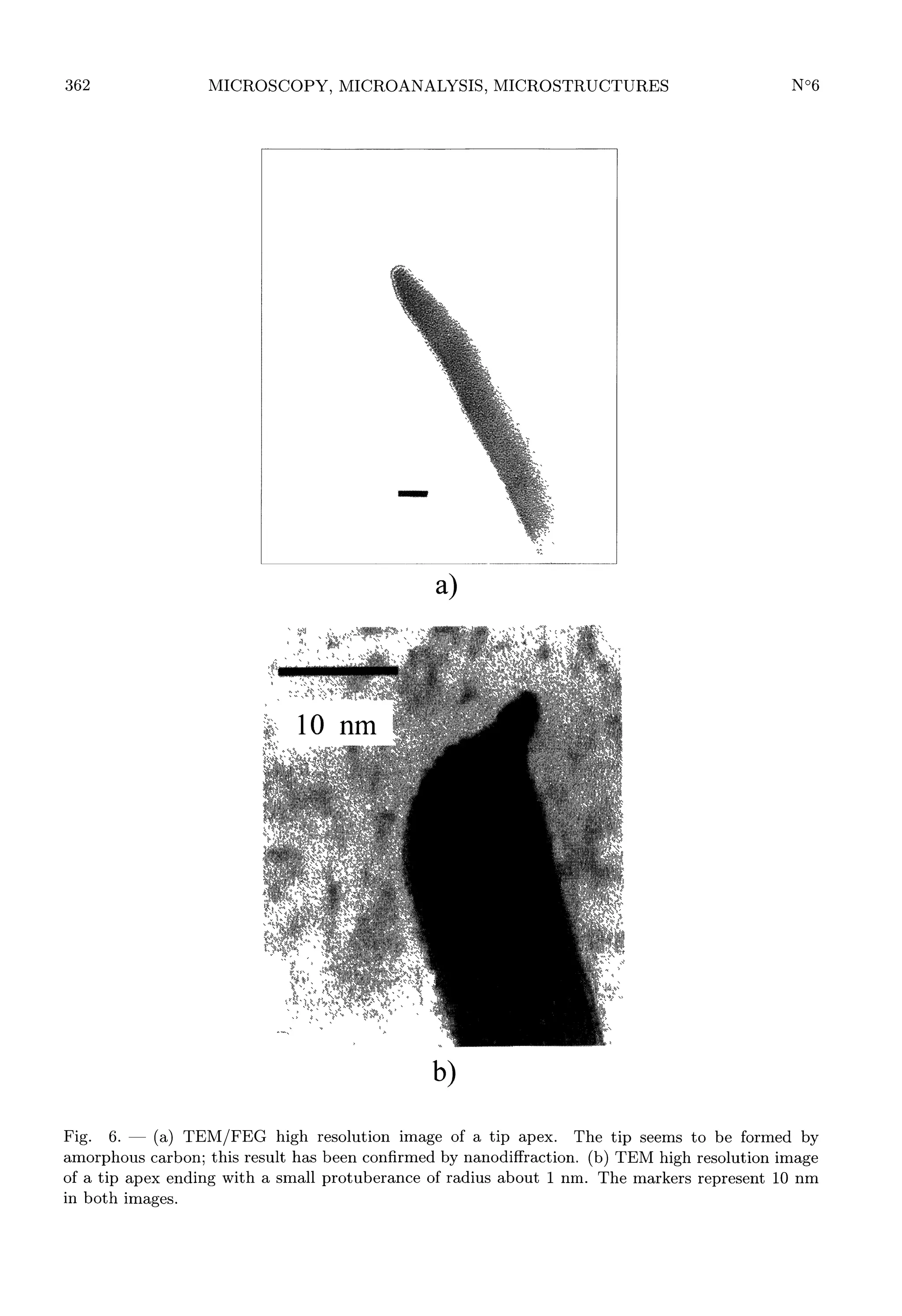
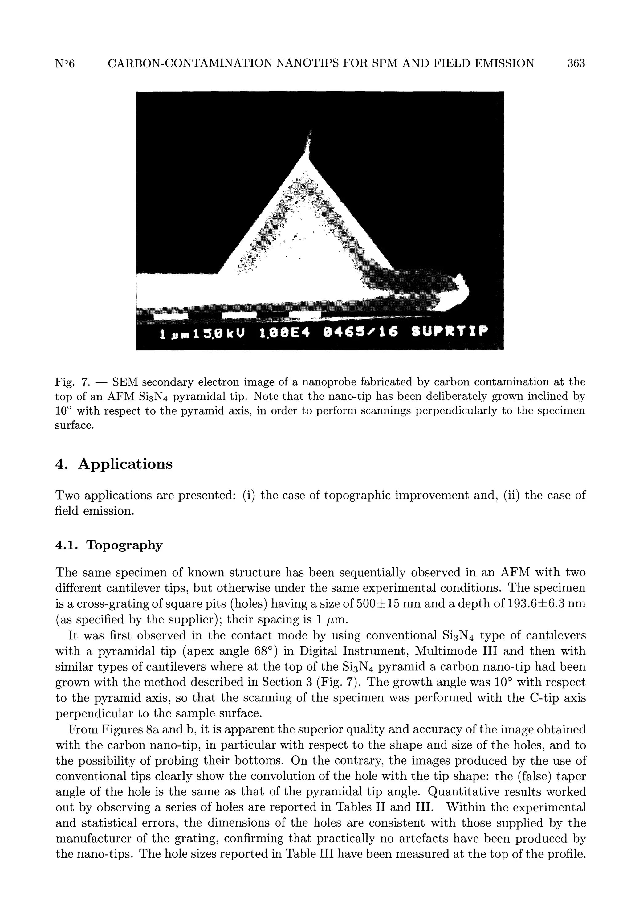
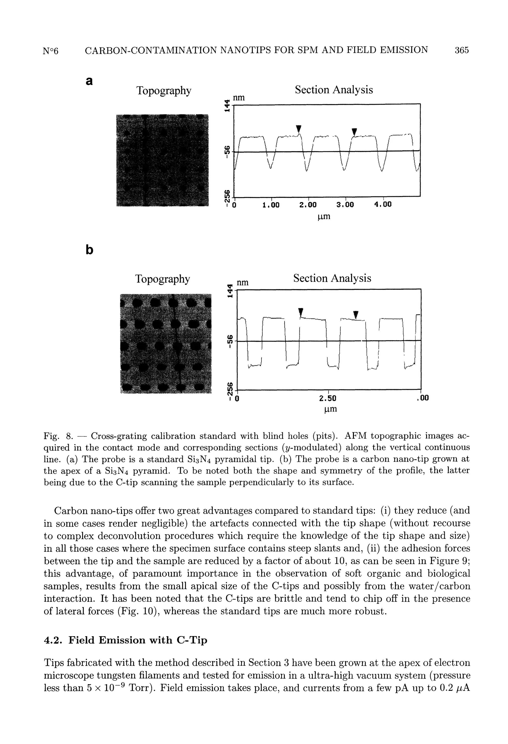
![367
10.
SEM secondary electron image of latex spheres deposited
after several observations in an AFM. To be noted the two broken
The marker represents 1 03BCm.
Fig.
-
gold-coated graphite surface
tips lying near the large sphere.
on a
contaminant, and controlled focusing and astigmatism correction during the tip growth. The
results can be immediately assessed.
Probes can be prepared with this technique in about 60 s; they have a conical shape with
the full angle as small as 10° and the length of 1 /mi. However, the height can be varied within
a large range (from less than 1 ,um to several tens of 03BCm) by varying the contamination time.
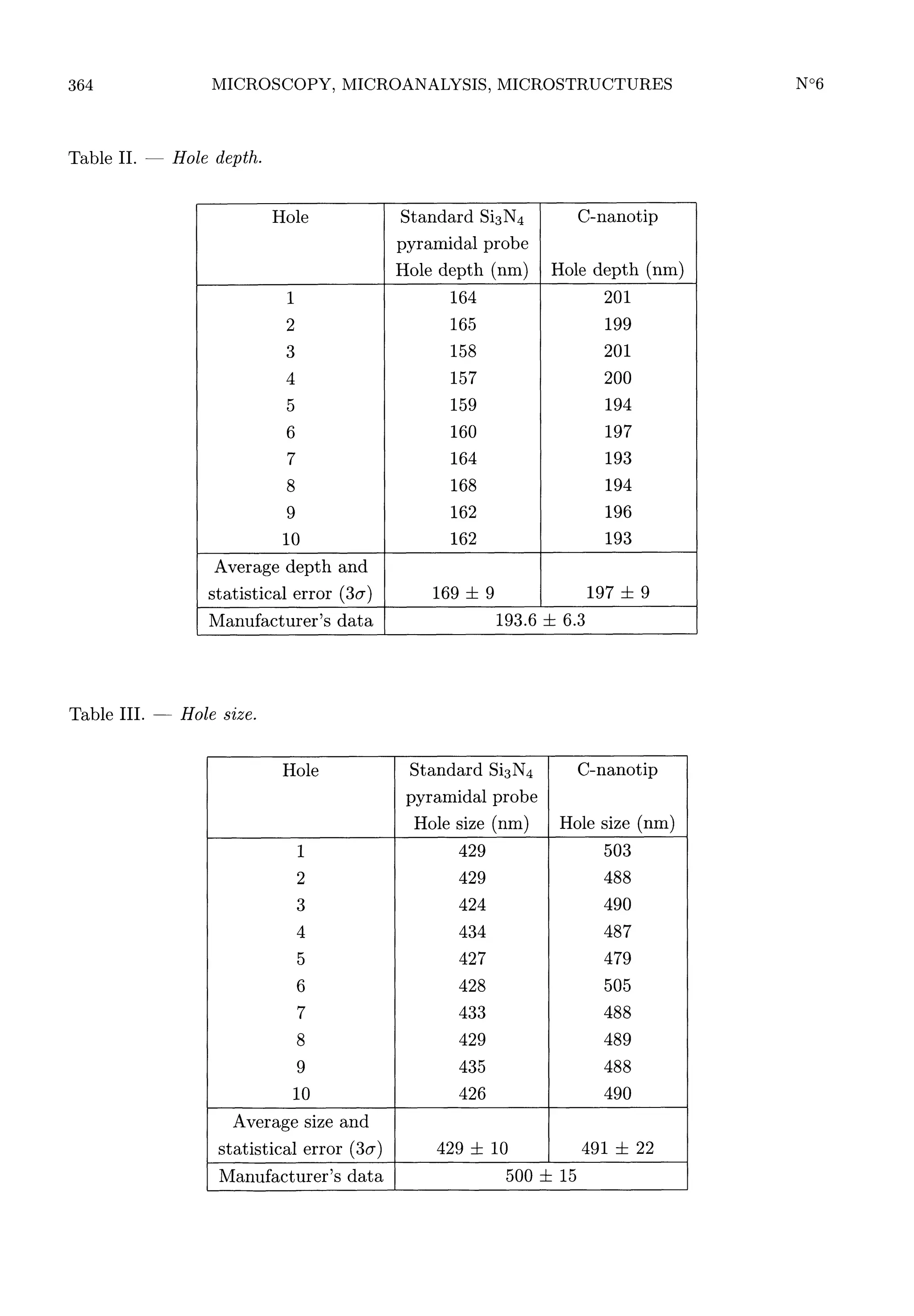
An example of application in the imaging and measurement of depth and size of blind holes
has been given and comparison has been made to the case of using standard tips. It has also
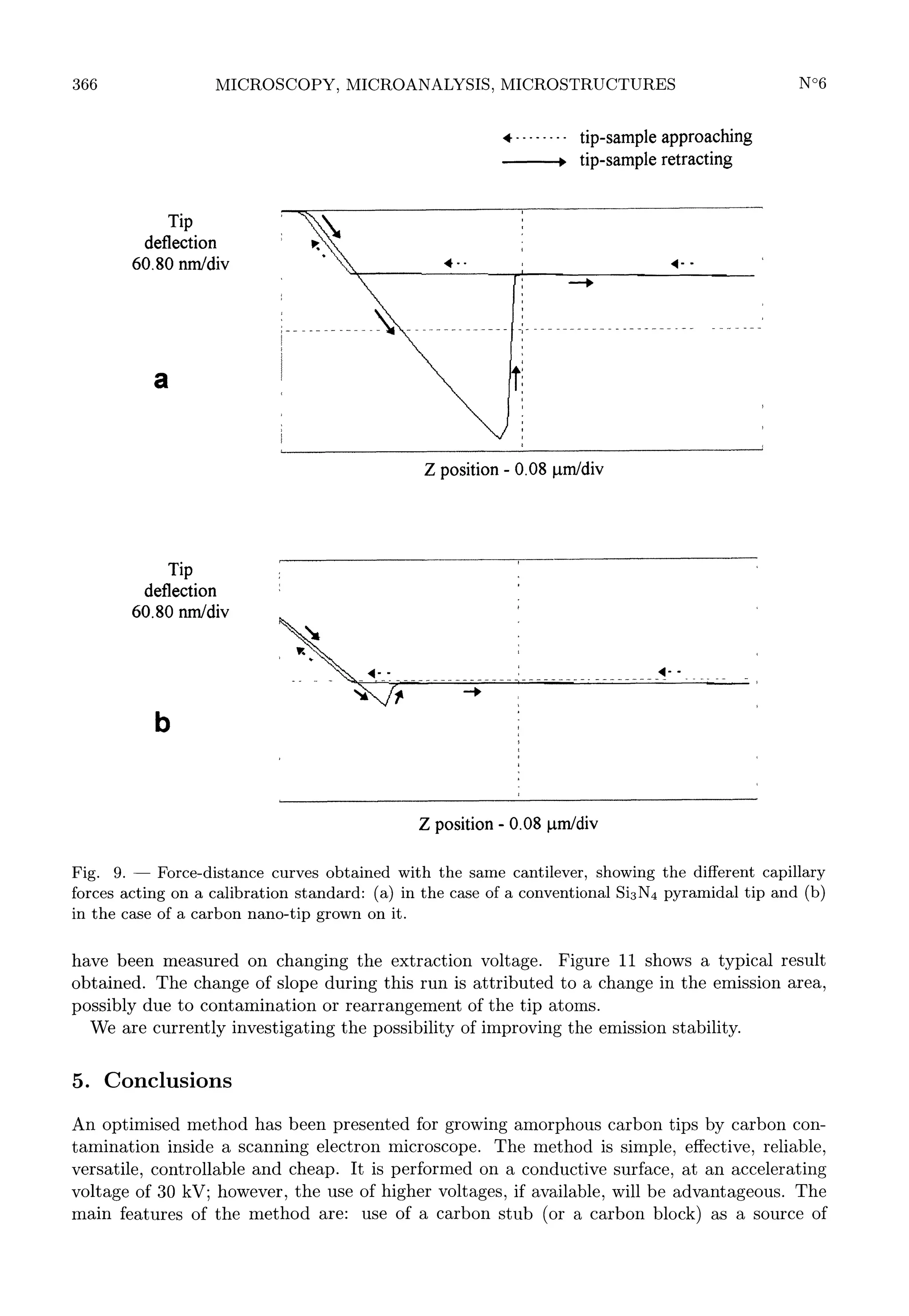
been shown that the capilary forces acting on a carbon nano-tip are smaller by one order of
magnitude with respect to those acting on standard tips under the same conditions.
Nano-tips made by carbon contamination (radius less than 5 nm) have been grown at the
apex of ordinary electron microscope tungsten filaments, and field emission has been demonstrated to take place; its features are similar to those obtained with pointed tungsten filaments
under the same geometrical conditions. However, current instabilities are a problem, which
are believed to be related to the pressure in the field emission chamber, around 5 x 10⁻⁹ Torr.
Modifications to the chamber to improve the vacuum are in progress.
We envisage the exploitation of such arrangements in electron microscopes equipped with
field emission guns. The use of standard pointed-filament (with their own sockets) at the
top of which carbon nano-tips are grown under controlled conditions in a scanning electron
microscope will allow their re-utilization in TEM/FEGs or in STEMs without the need to
change neither the configuration of the gun electrodes, nor the related electronics, as might be
required for re-sharpening blunt tungsten tips for field emission guns [12]. Carbon tips grown
on an electrically conducting substrate may also be used in scanning tunneling microscopy.](https://image.slidesharecdn.com/microscopymicroanalysismicrostructurestheeuropeanphysicaljournalappliedphysicsnanotechnologysentimen-131230173200-phpapp01/75/Microscopy-microanalysis-microstructures_the-european-physical-journal_applied-physics_nanotechnology_sentimenti-13-2048.jpg)
![368
Experimental Fowler-Nordheim plot obtained from a carbon-contamination grown nanofield emitter at a pressure of less than 5 x 10-g Torr. At 2600 V the emission current is
2.6 nA. The two trends are attributed to emission changes due to contaminants or geometrical changes.
Fig. Il.
tip used
-
as
Acknowledgments
We thank Dr A. Alessandrini for useful discussions and MURST for financial support.
References
[1] Keller D.J. and Chou C.-C., Surf. Sci. 268 (1992) 333.
[2] Fink H.W., Phys. Scr. 38 (1988) 260.
[3] Binh V.T. and Garcia N., Ultramicroscopy 42-44 (1992) 80.
[4] Baptist R., Proc. 7th Int. Vacuum Microelectronics Conf., Grenoble (Société Française du
Vide, Paris, 1994).
[5] Rinzler A.S., Hafner J.H., Nikolaev P., Lou L., Kim S.G., Tomanek D., Nordlander P.,
Colbert D.T. and Smalley R.E., Science 269 (1995) 1150.
[6] De Heer W.A., Châtelain A. and Ugarte D., Science 270 (1995) 1179.
[7] Randi M.R., Monteverde F.T. and Valdrè U., J. Supercond. Sci. Technol. 7 (1994) 507.
[8] Hart K.R., Kassner T.F. and Maurin J.K., Phil. Mag. 21 (1970) 453.
[9] Hirsch P., Kässens M., Püttmann M. and Reimer L., Scanning 16 (1994) 101.
[10] Sentimenti A., Thesis, no. 2091, Università degli Studi, Bologna, 1995.
[11] Antognozzi M. and Valdrè U., Microsc. Microanal. Microstruct. 6 (1995) 513.
[12] Binh V.T., Garcia N. and Purcell S.T., Adv. Imag. Elec. Phys. 95 (1996) 63.](https://image.slidesharecdn.com/microscopymicroanalysismicrostructurestheeuropeanphysicaljournalappliedphysicsnanotechnologysentimen-131230173200-phpapp01/75/Microscopy-microanalysis-microstructures_the-european-physical-journal_applied-physics_nanotechnology_sentimenti-14-2048.jpg)

This document describes a method for fabricating nano-sized carbon tips in a scanning electron microscope (SEM) using controlled carbon contamination. Key steps include: using a 30kV beam for highest contamination rate; smallest spot size (~5nm); stable, well-focused beam; and a carbon block nearby to increase carbon concentration. Tips with 10° aperture and ~5nm tip are produced in under 60 seconds. Successive focusing during growth produces tips shaped like stacked cones rather than a single paraboloid. The tips are used as probes in atomic force microscopy, achieving higher resolution than conventional probes due to their small size and shape. They are also used as field emitters for electron guns due to their nanoscale size and


