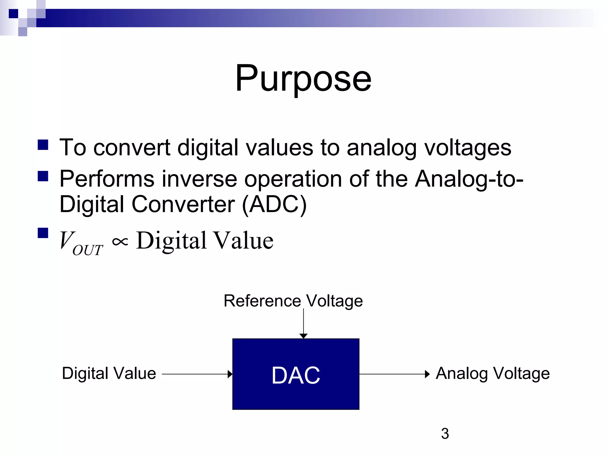
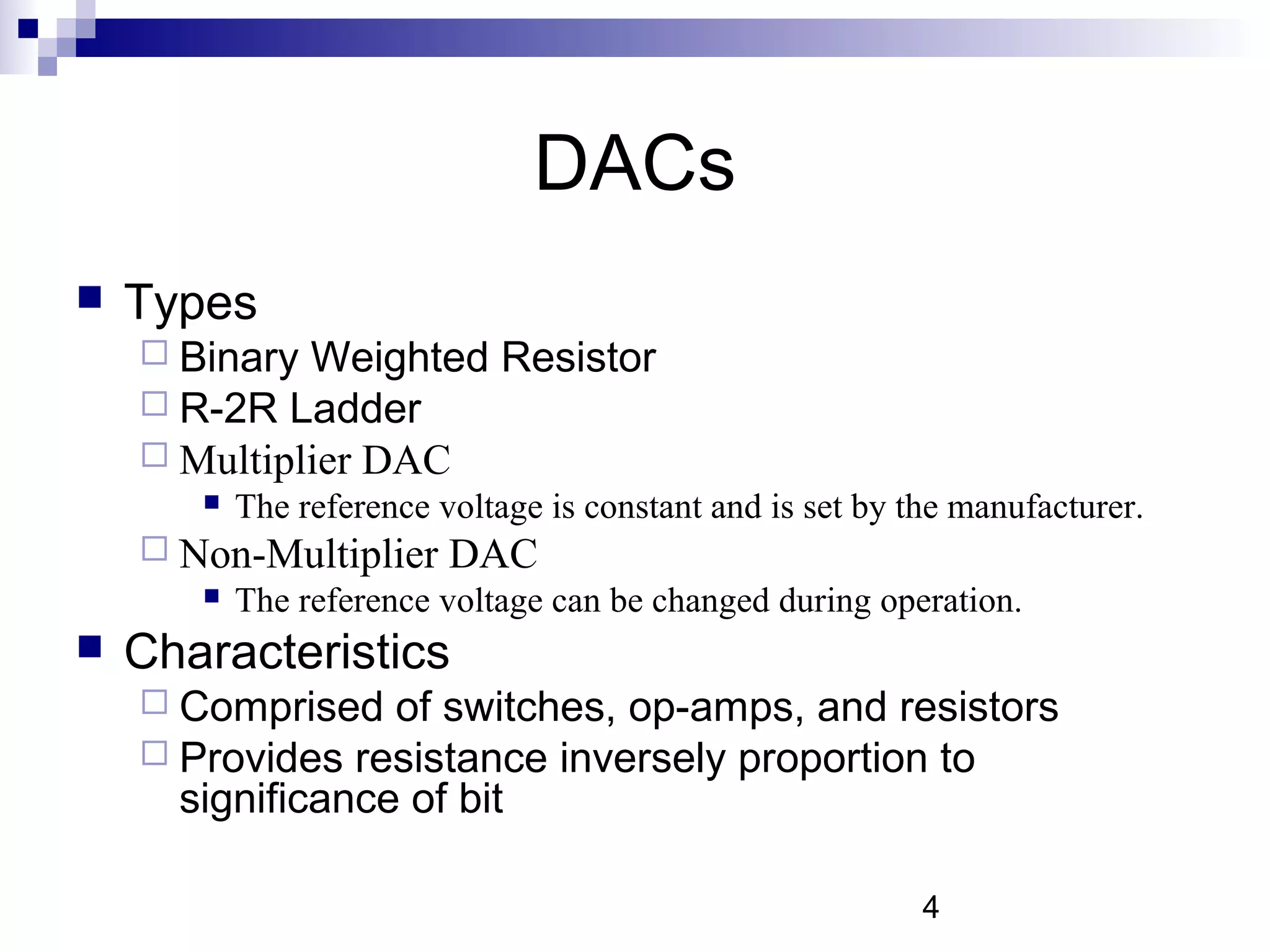
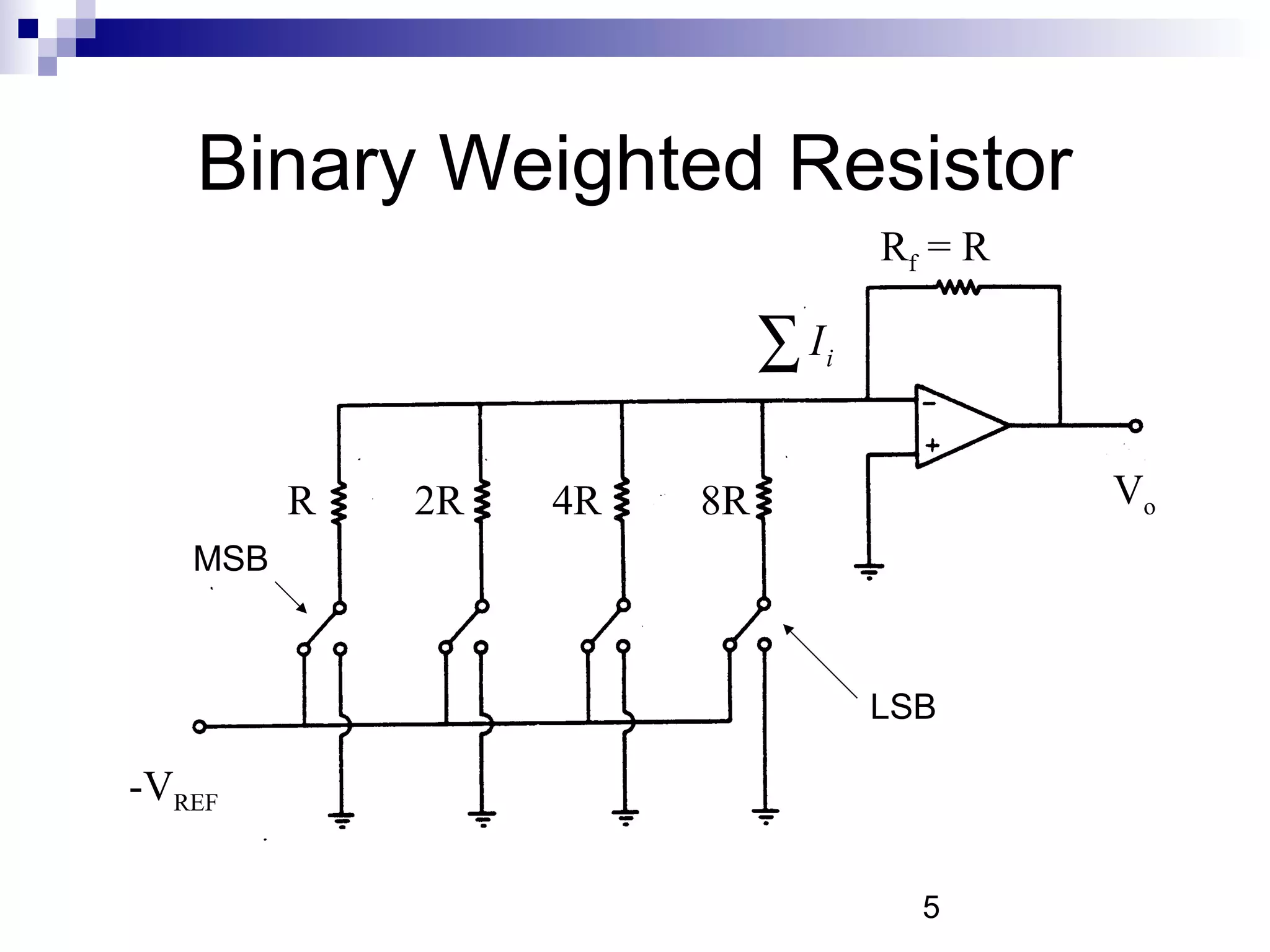
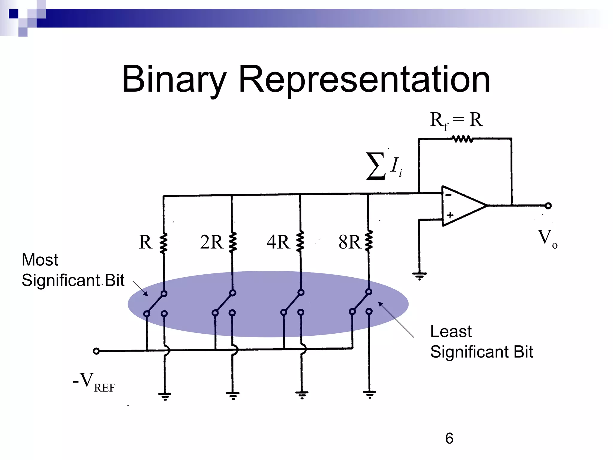
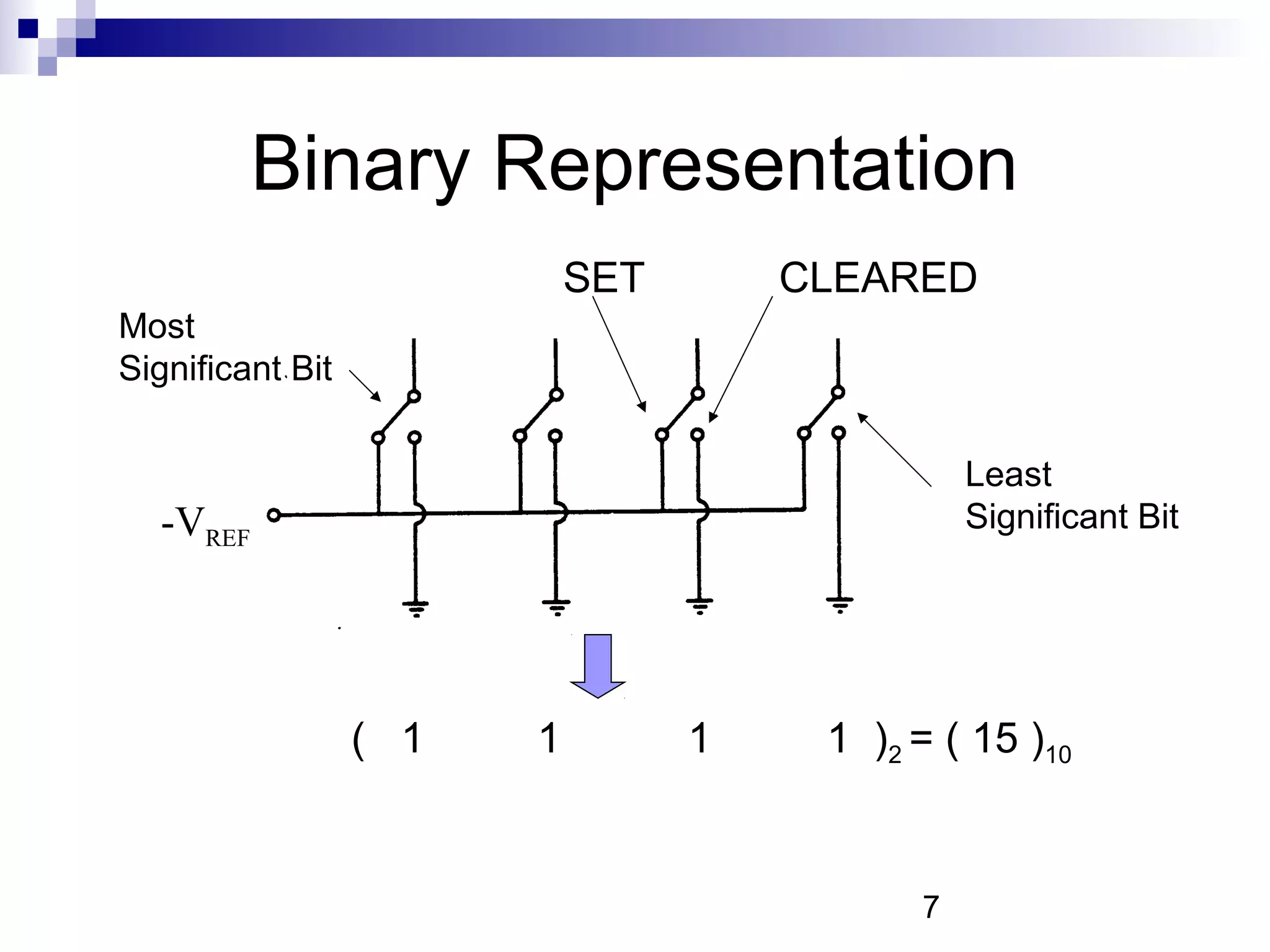
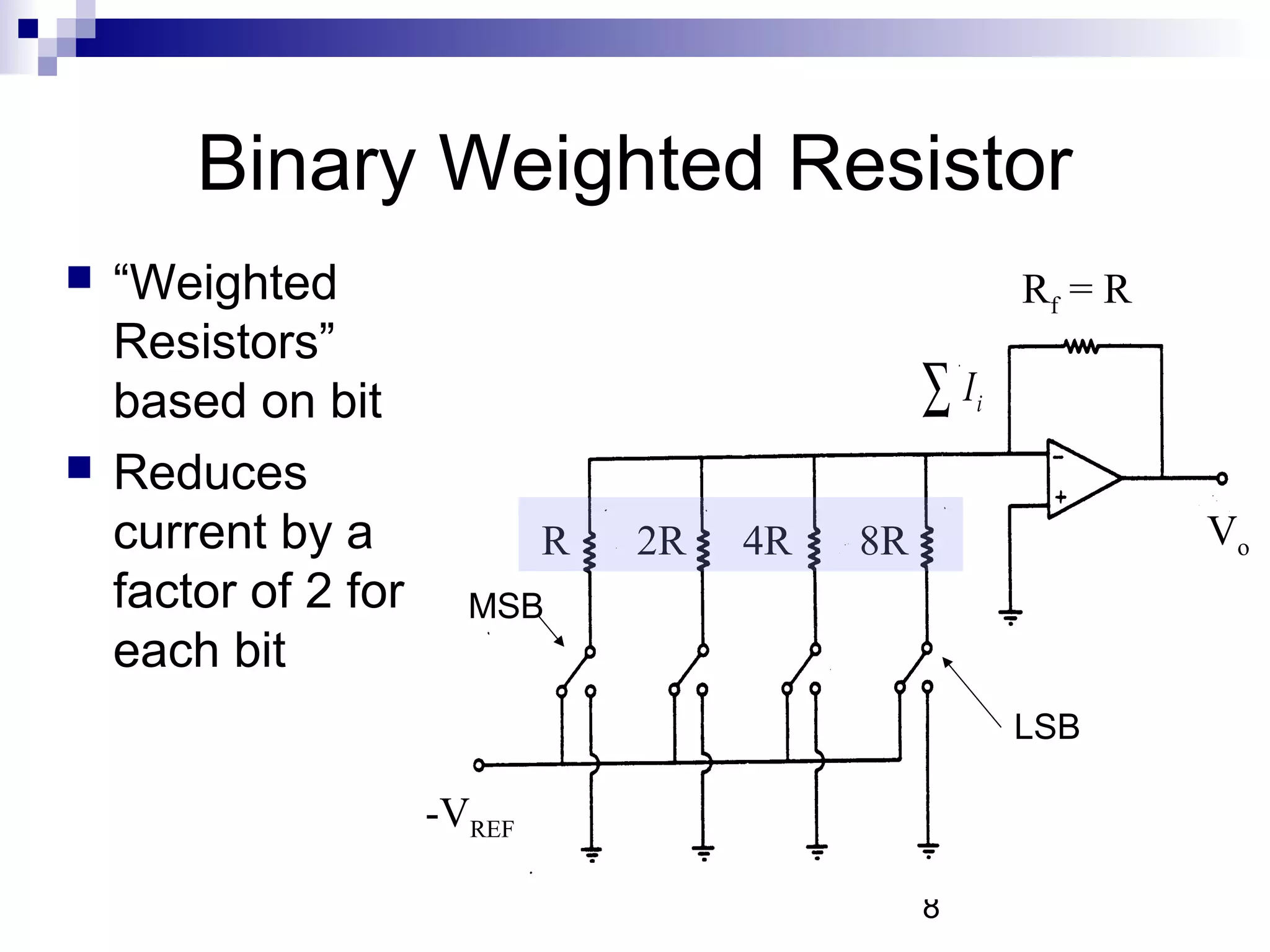
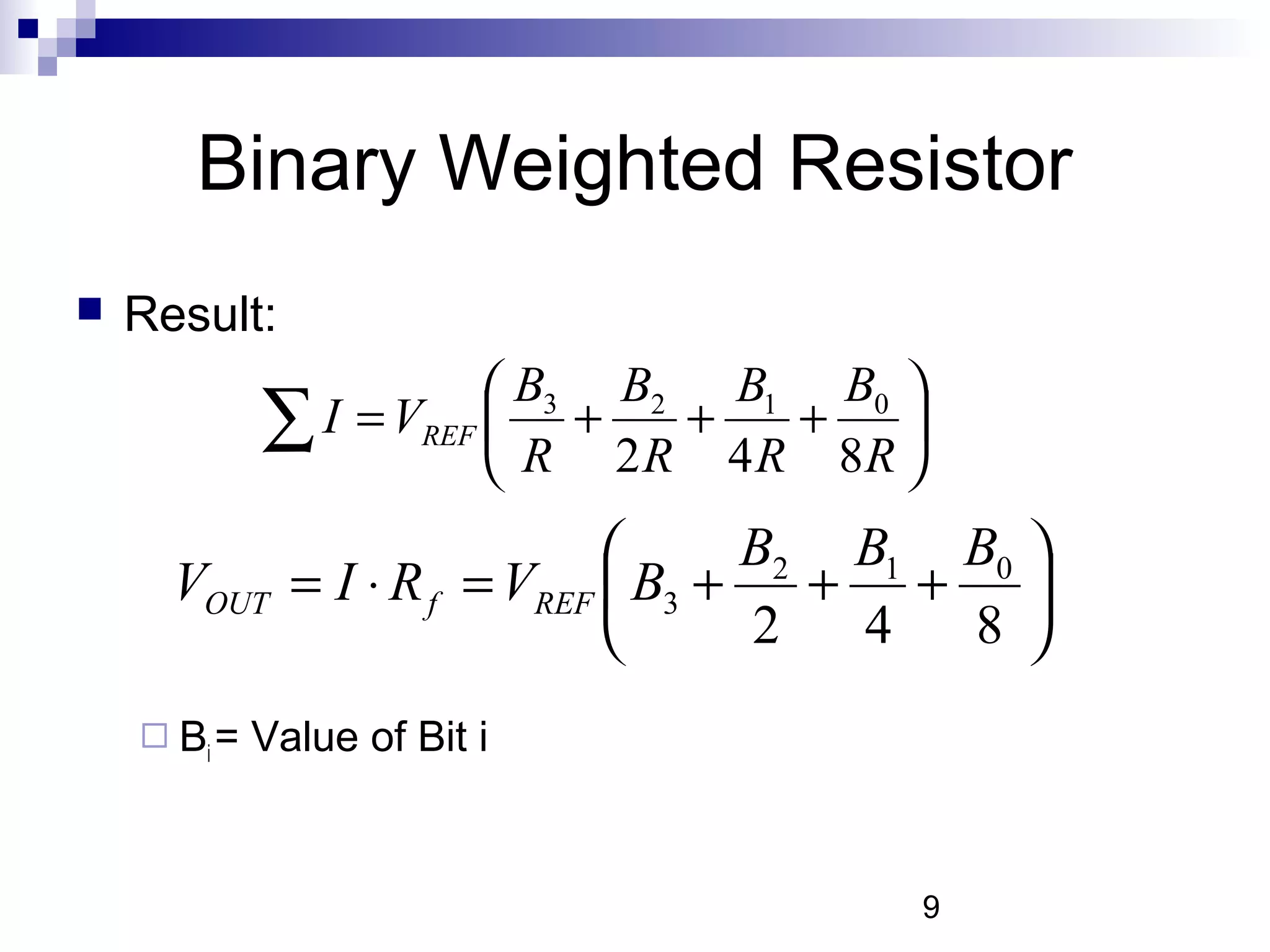
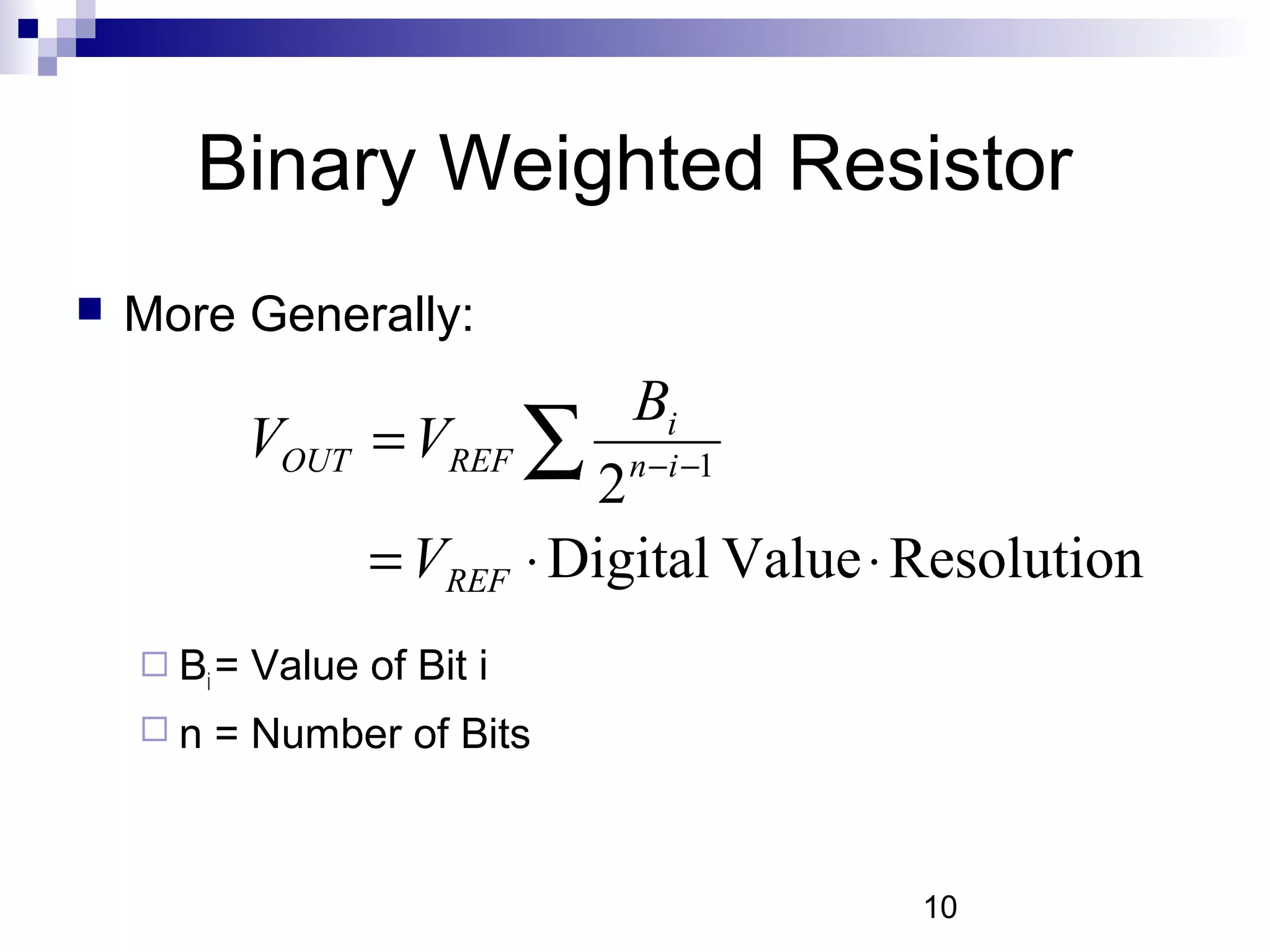
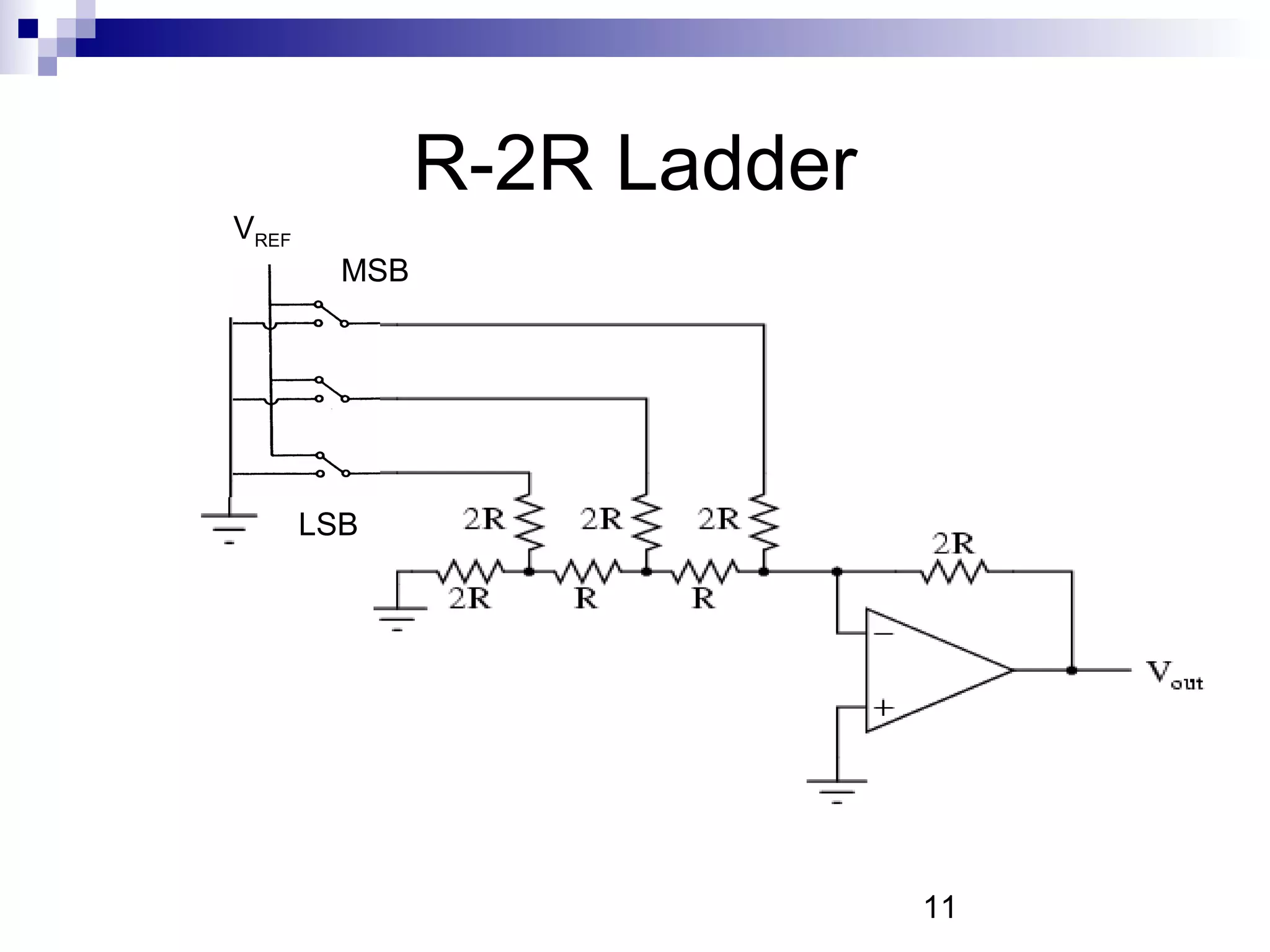
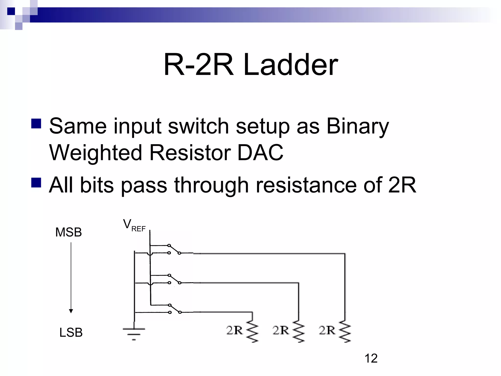
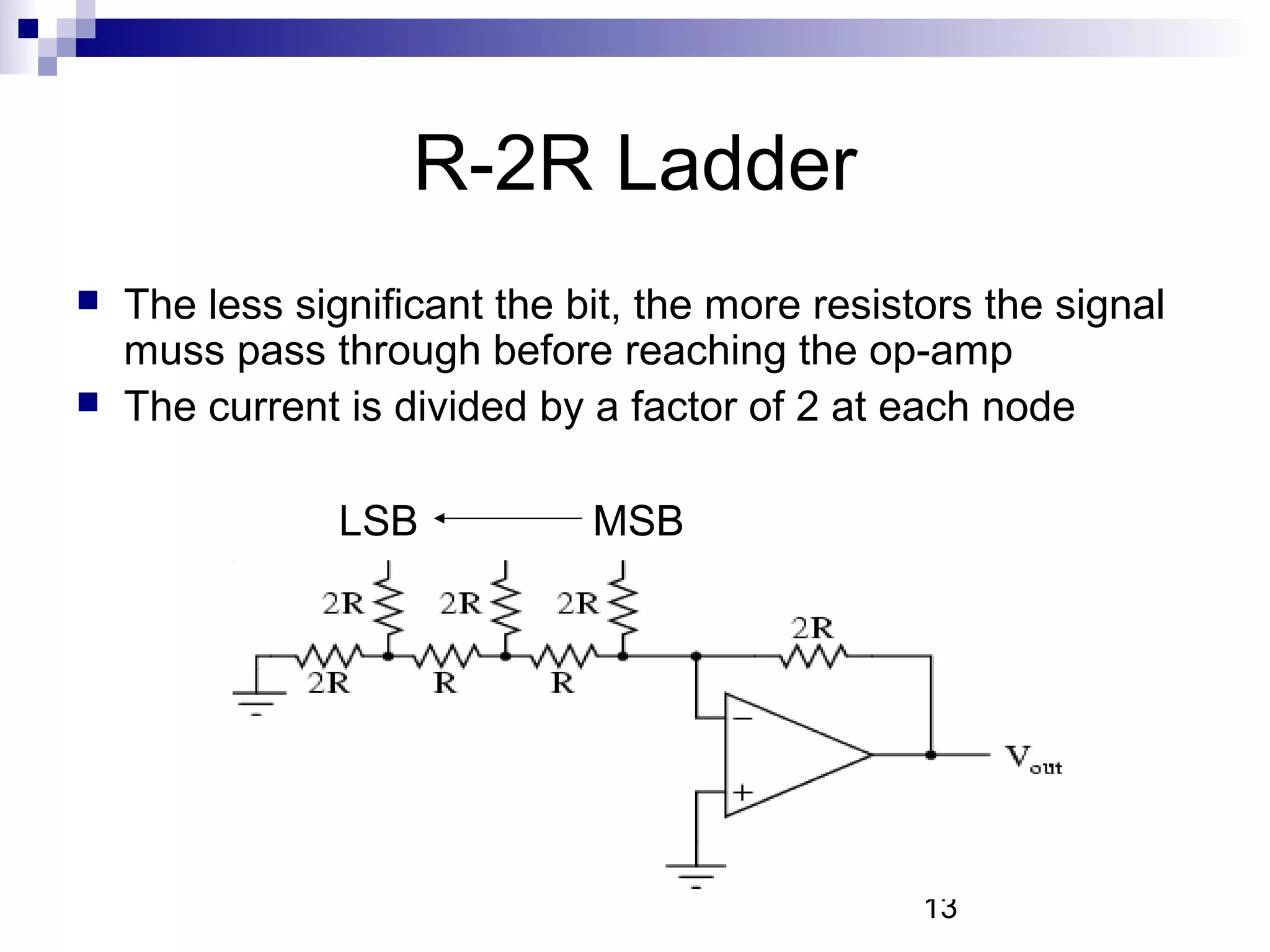
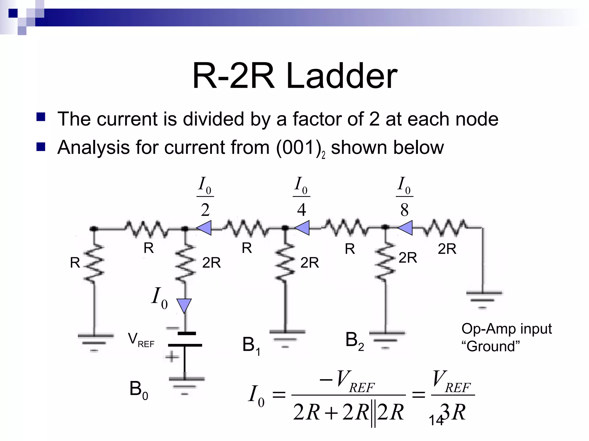
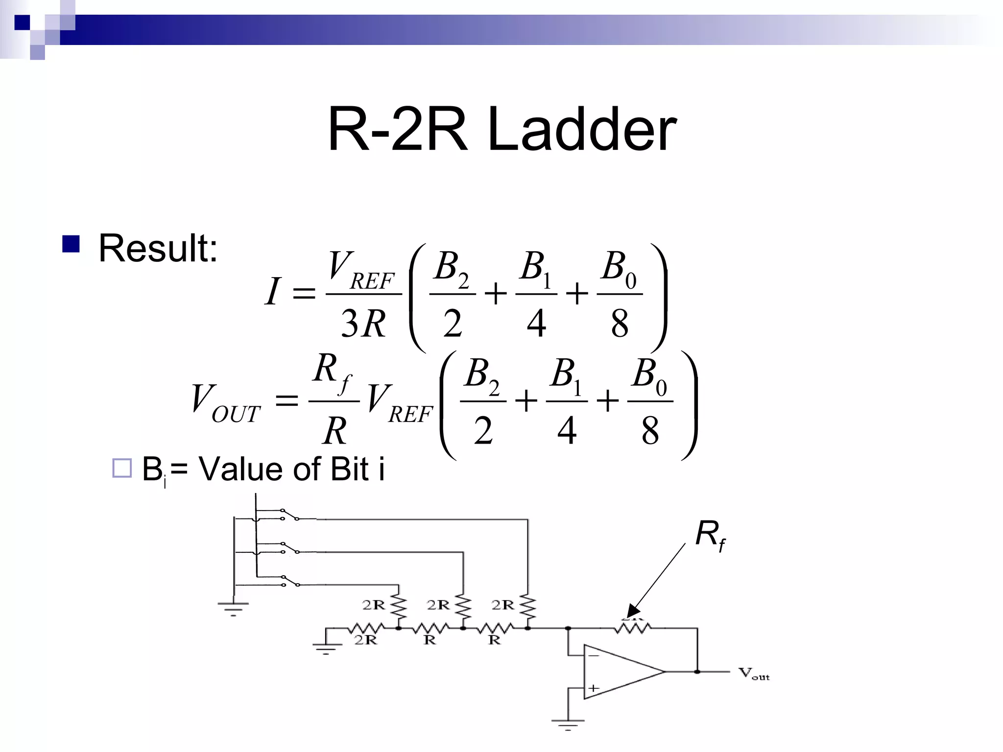
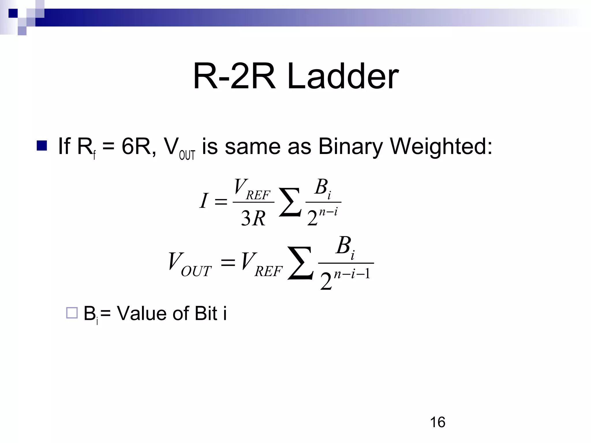
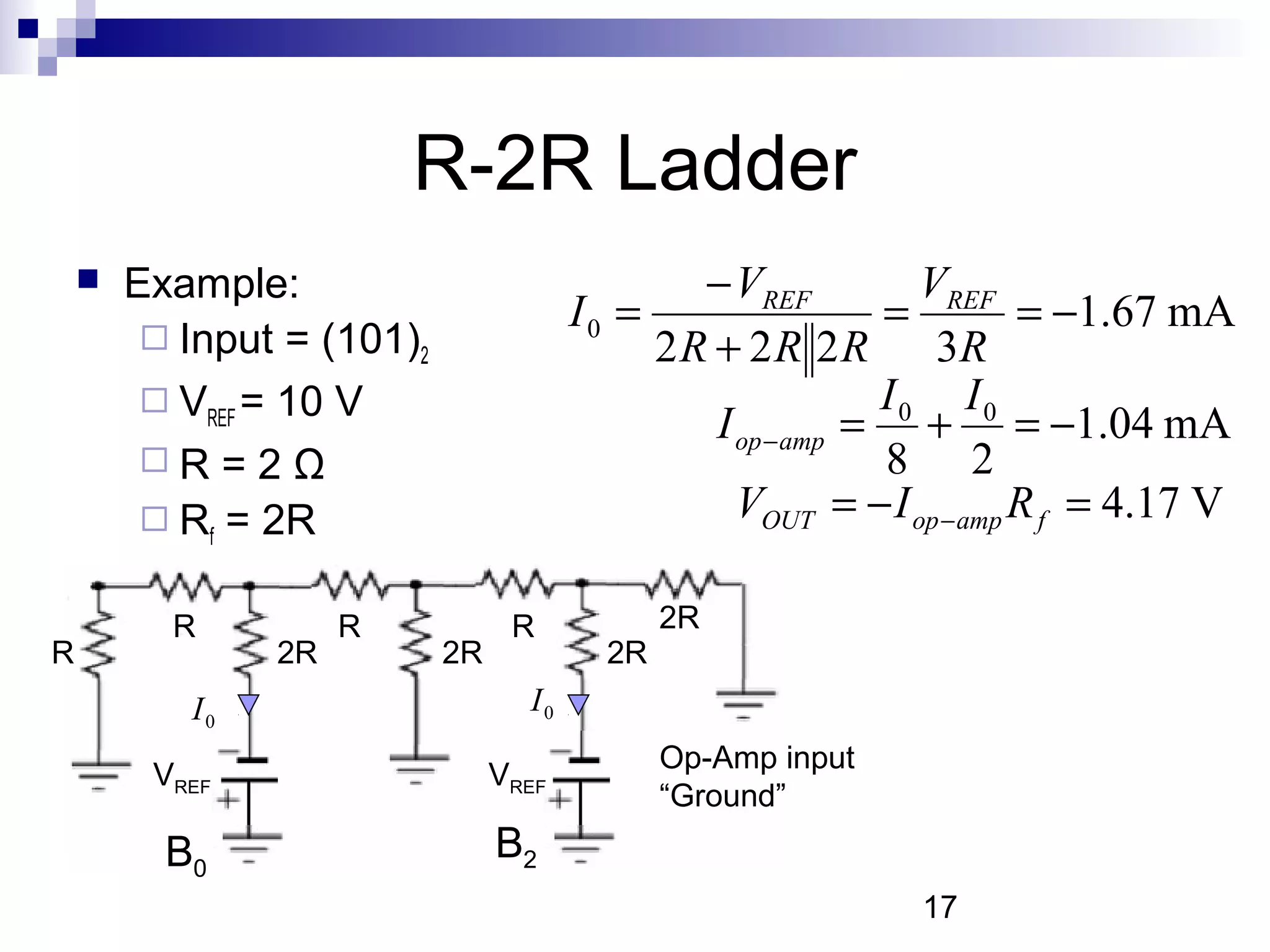
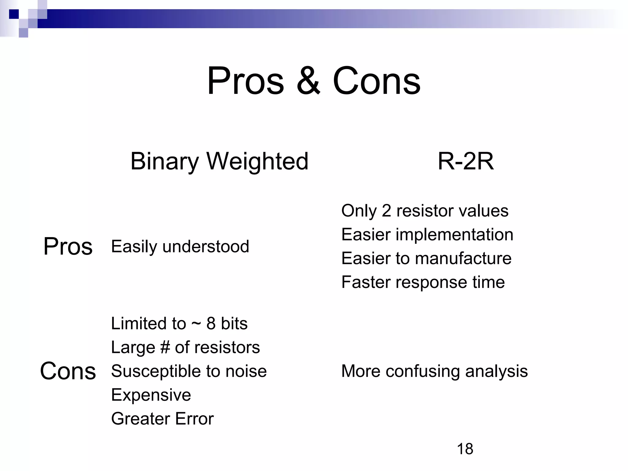
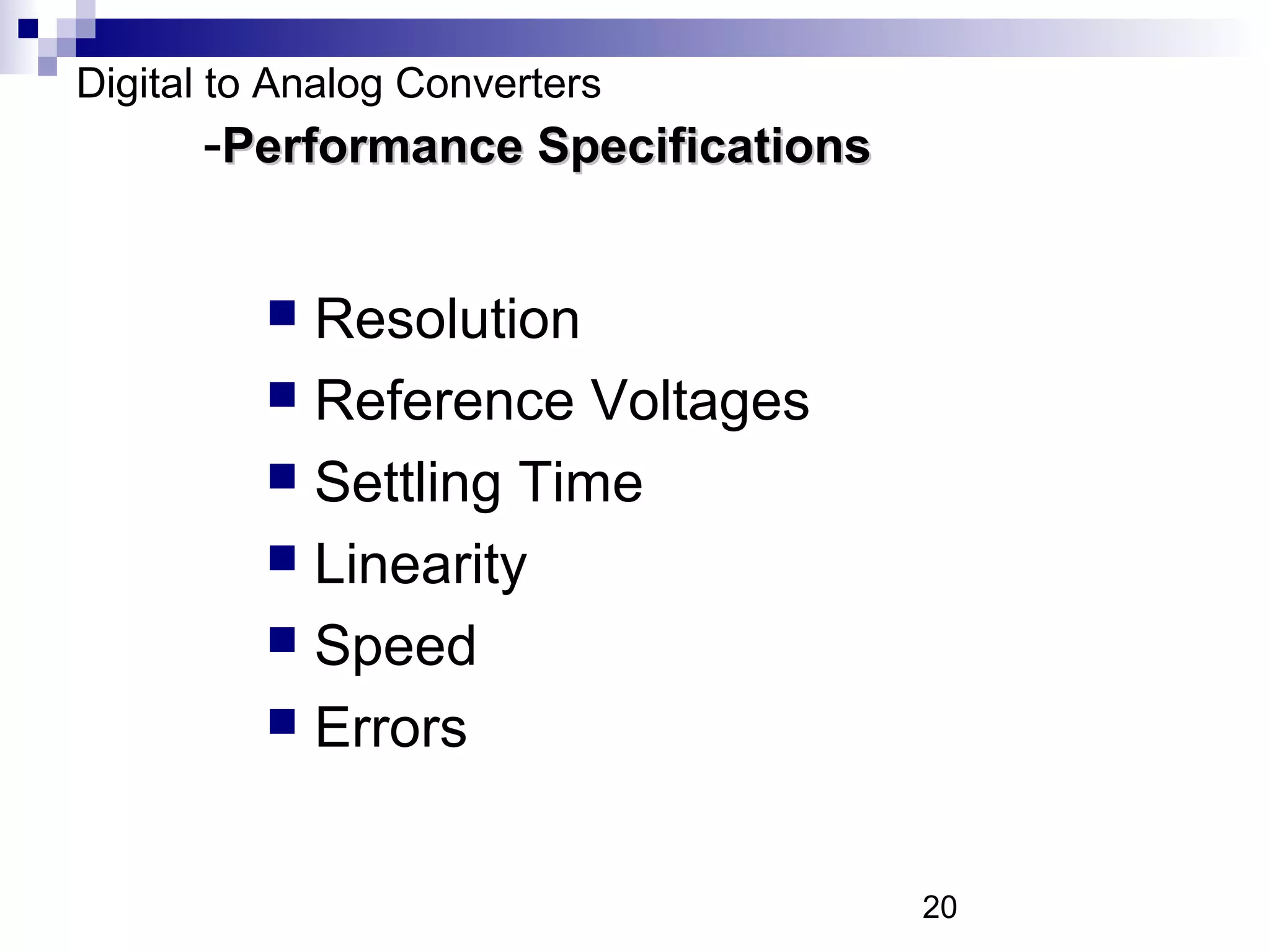
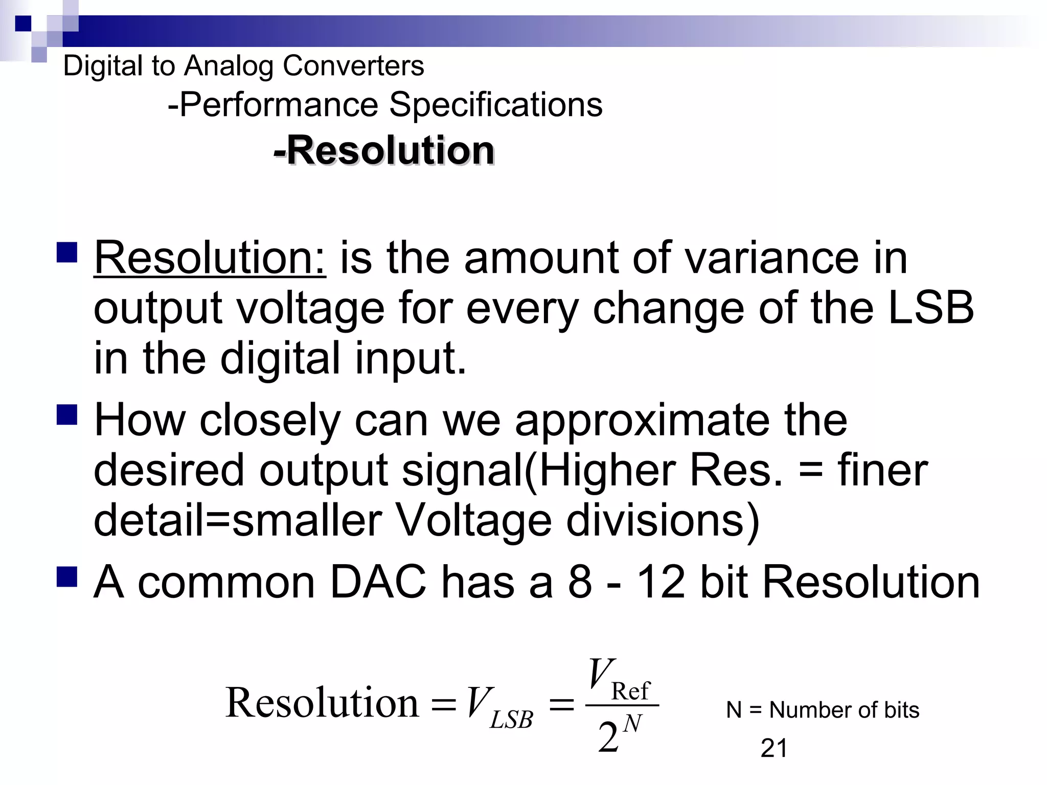
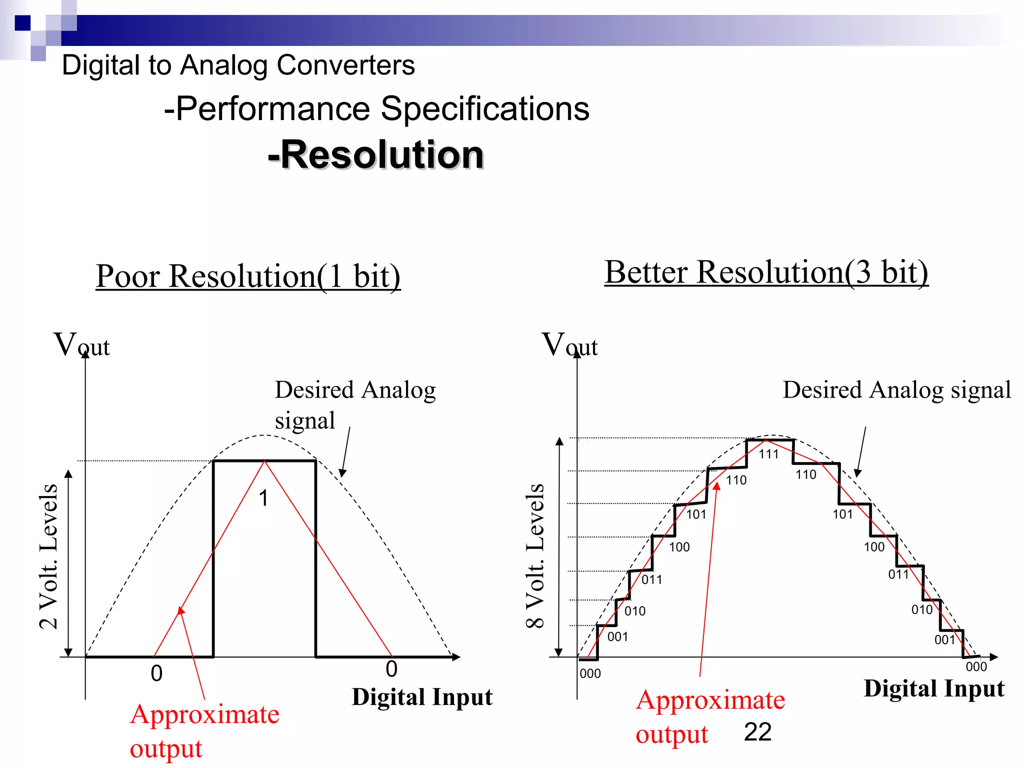
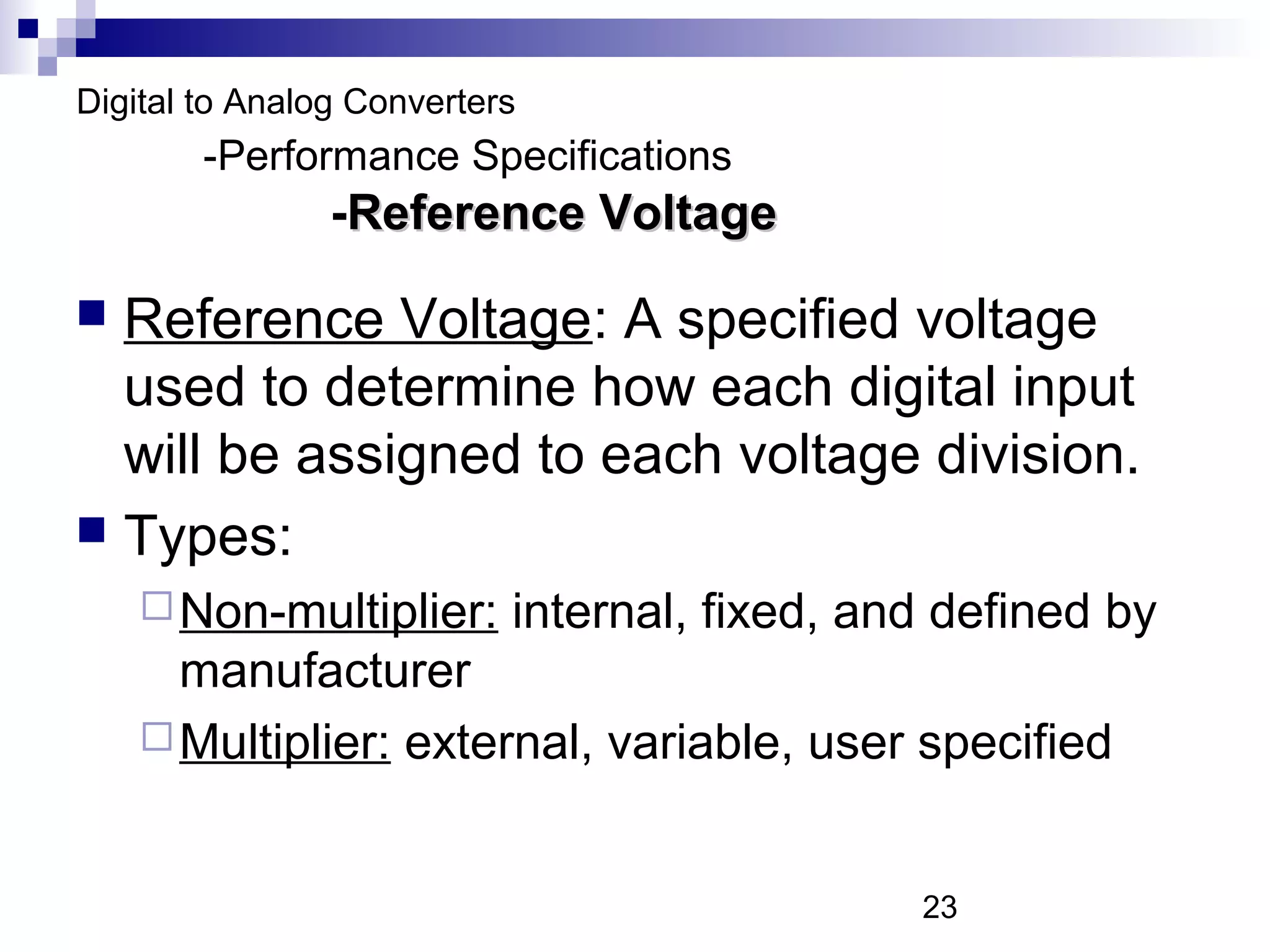
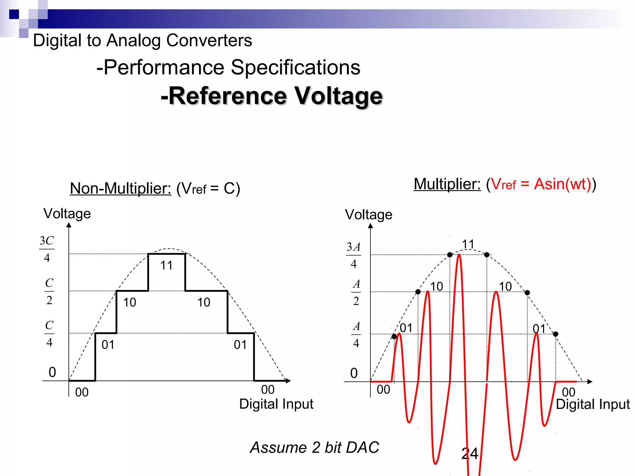
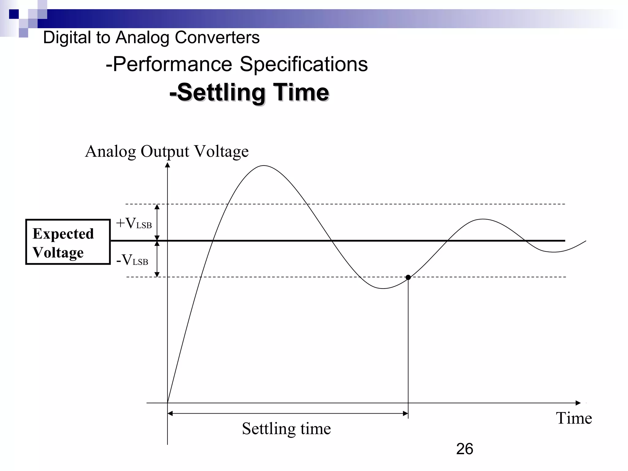
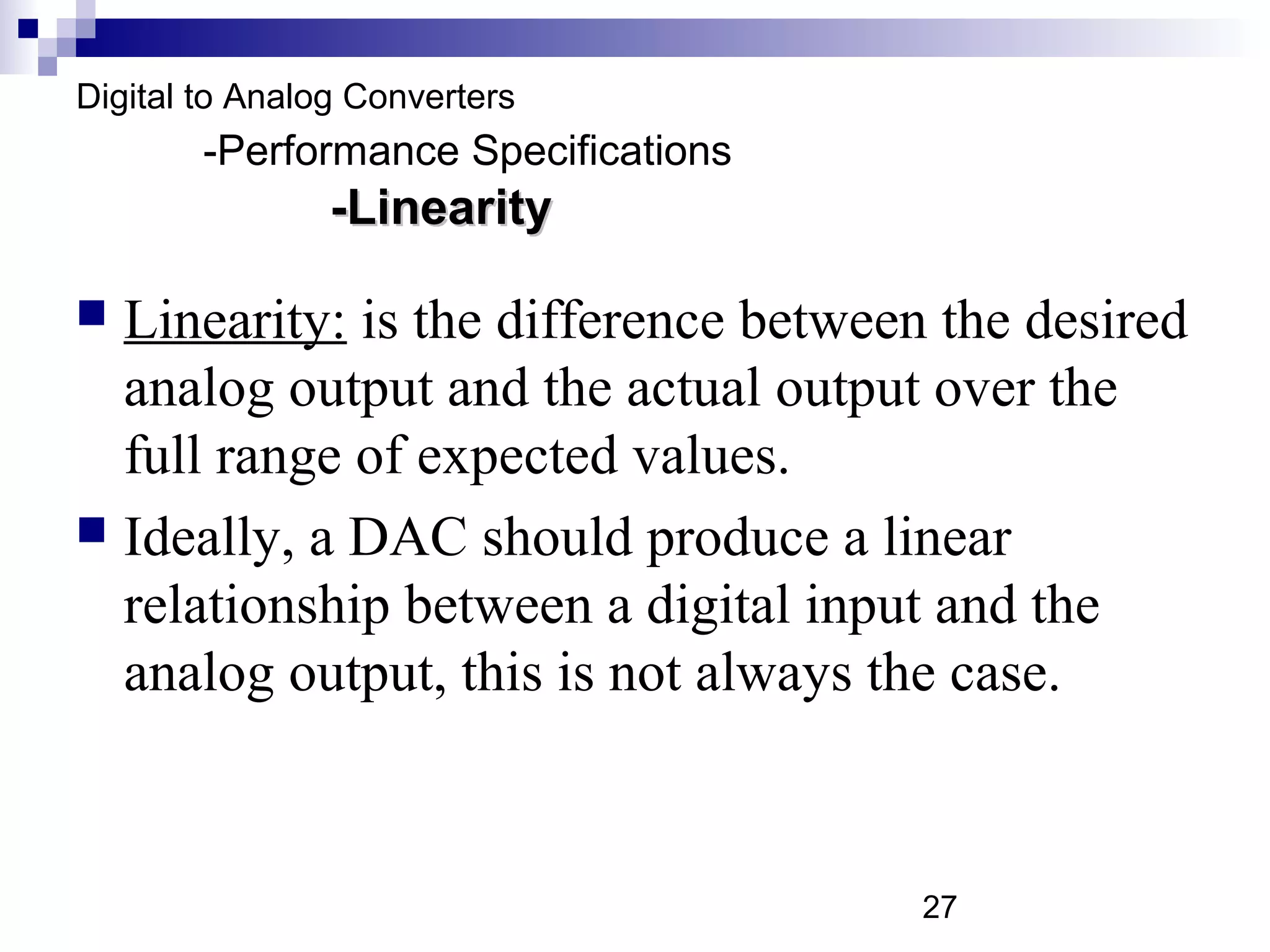
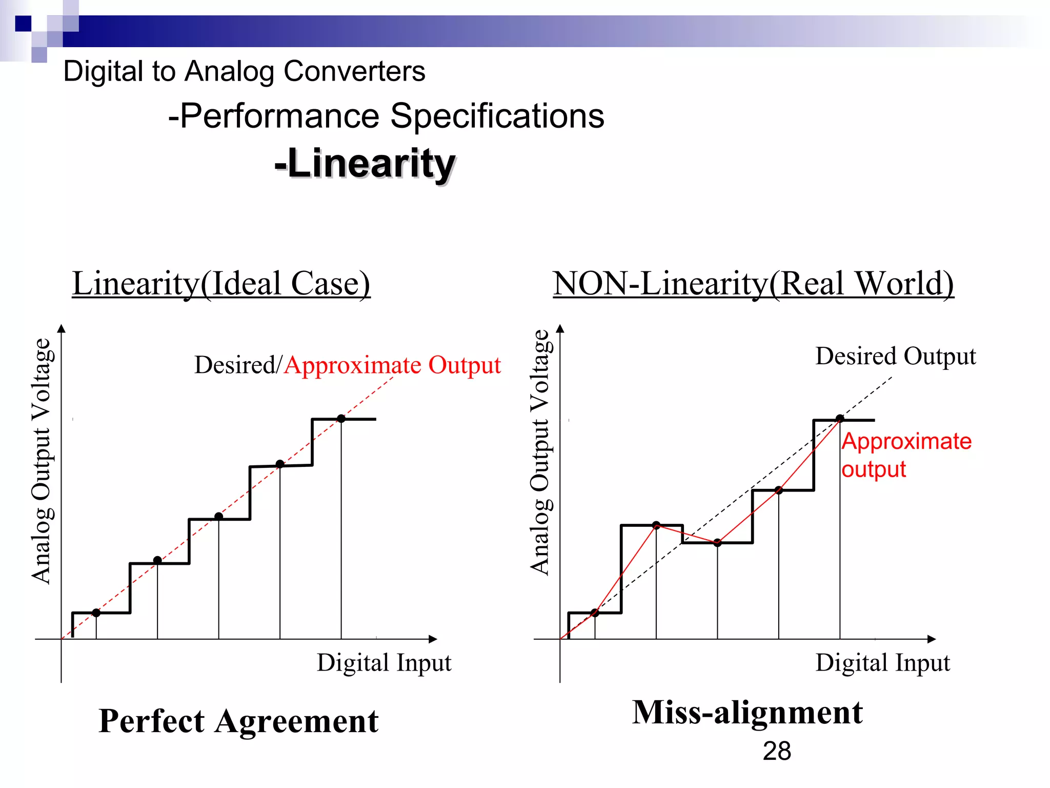
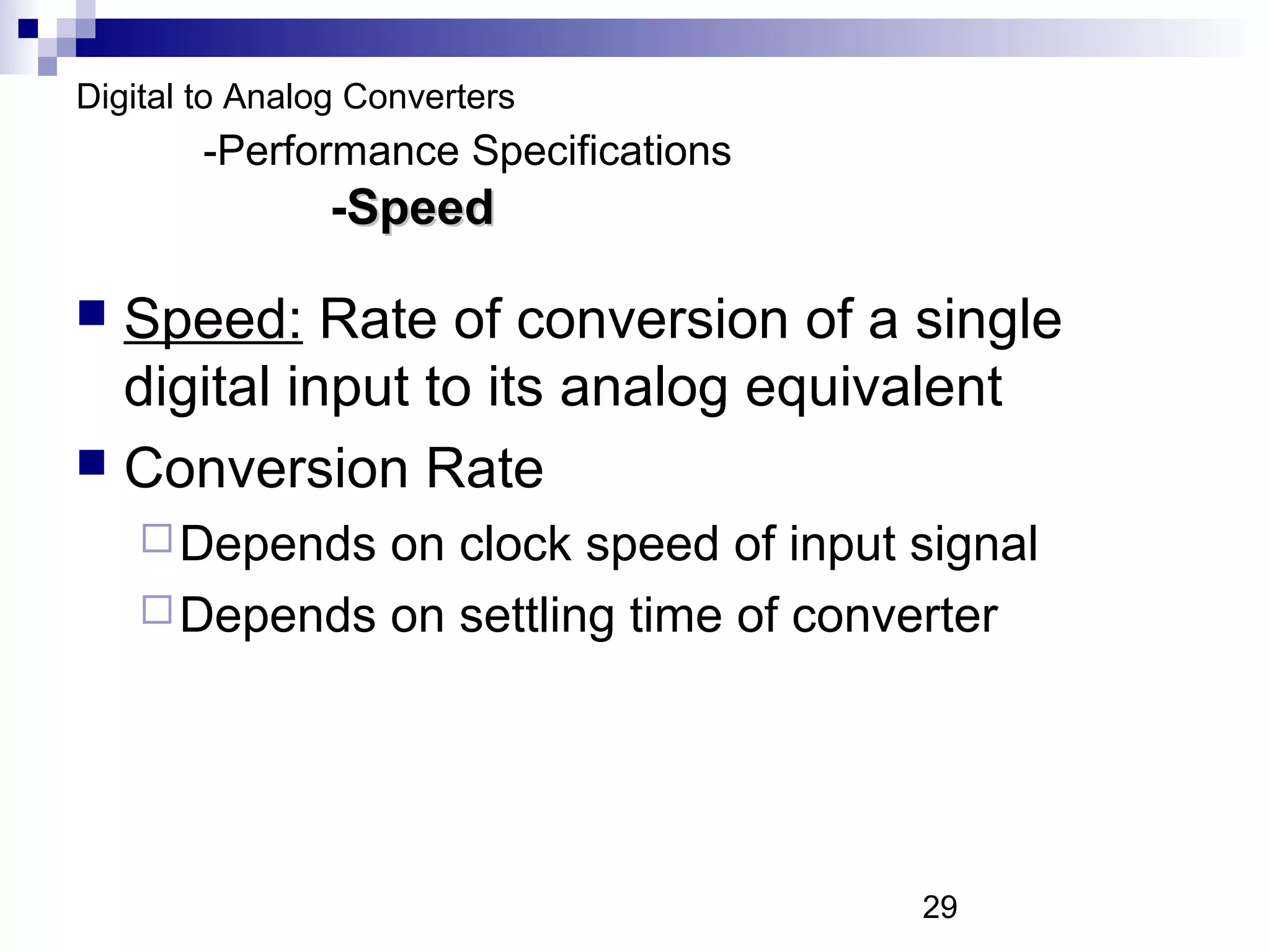
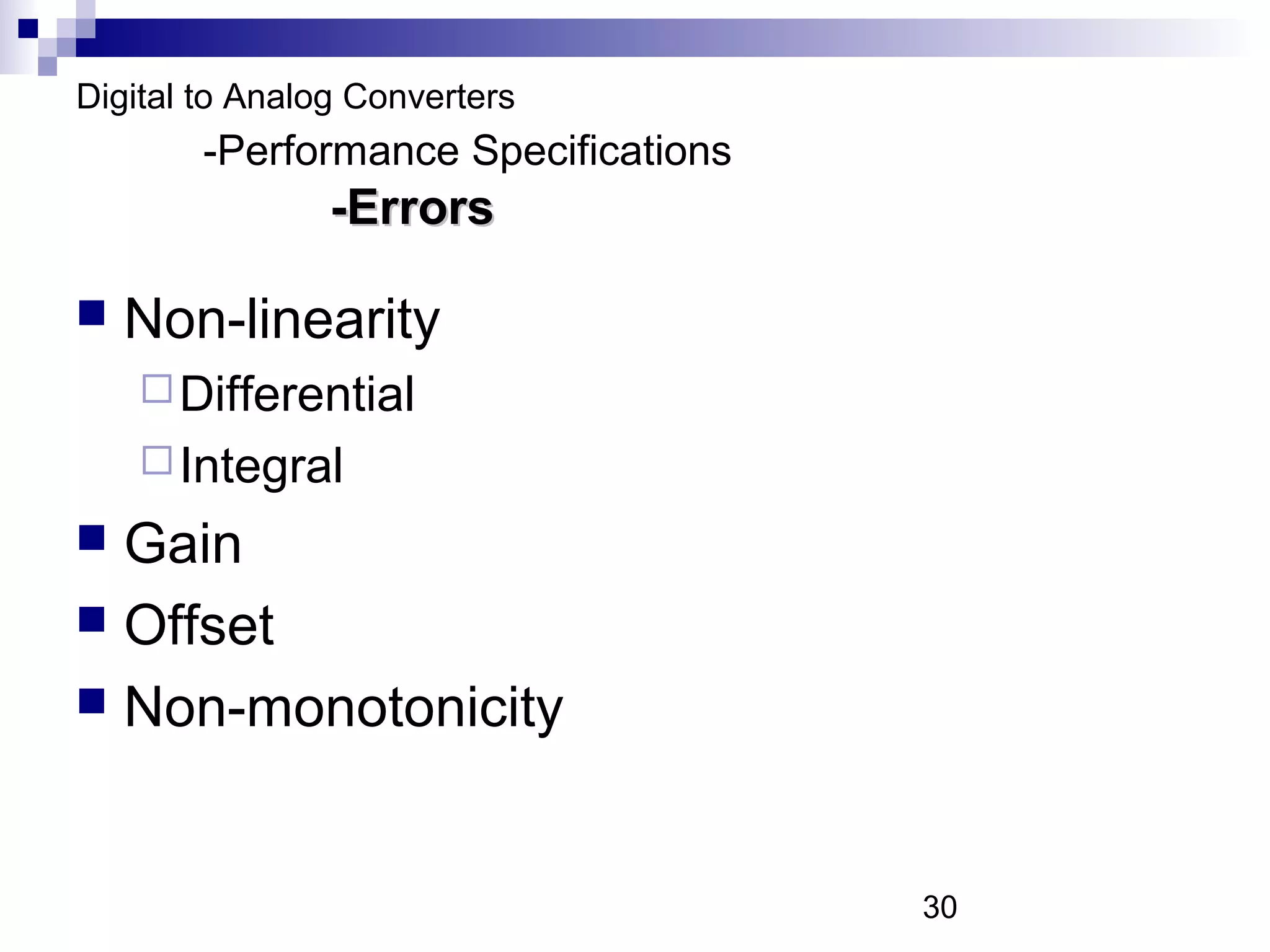
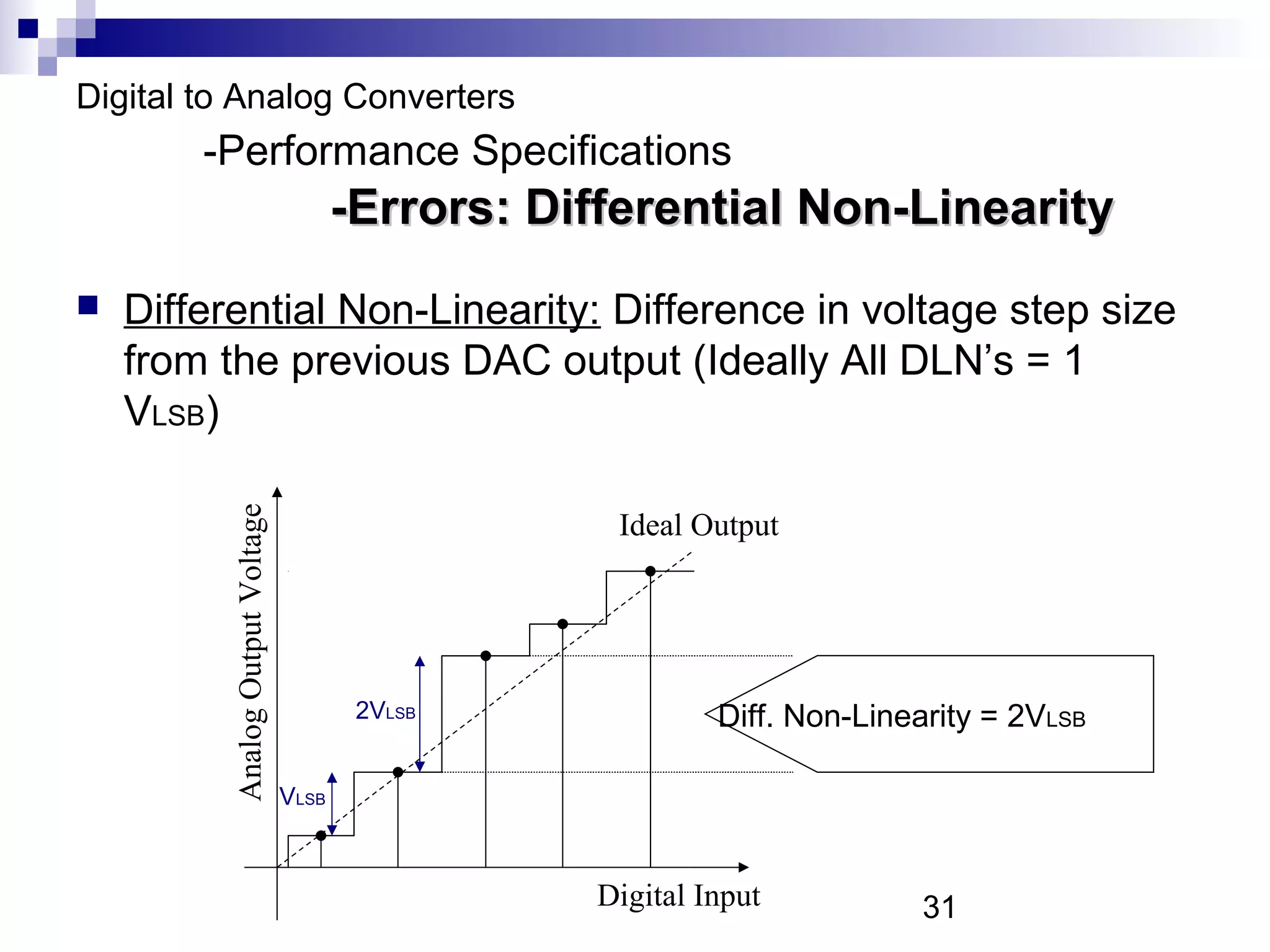
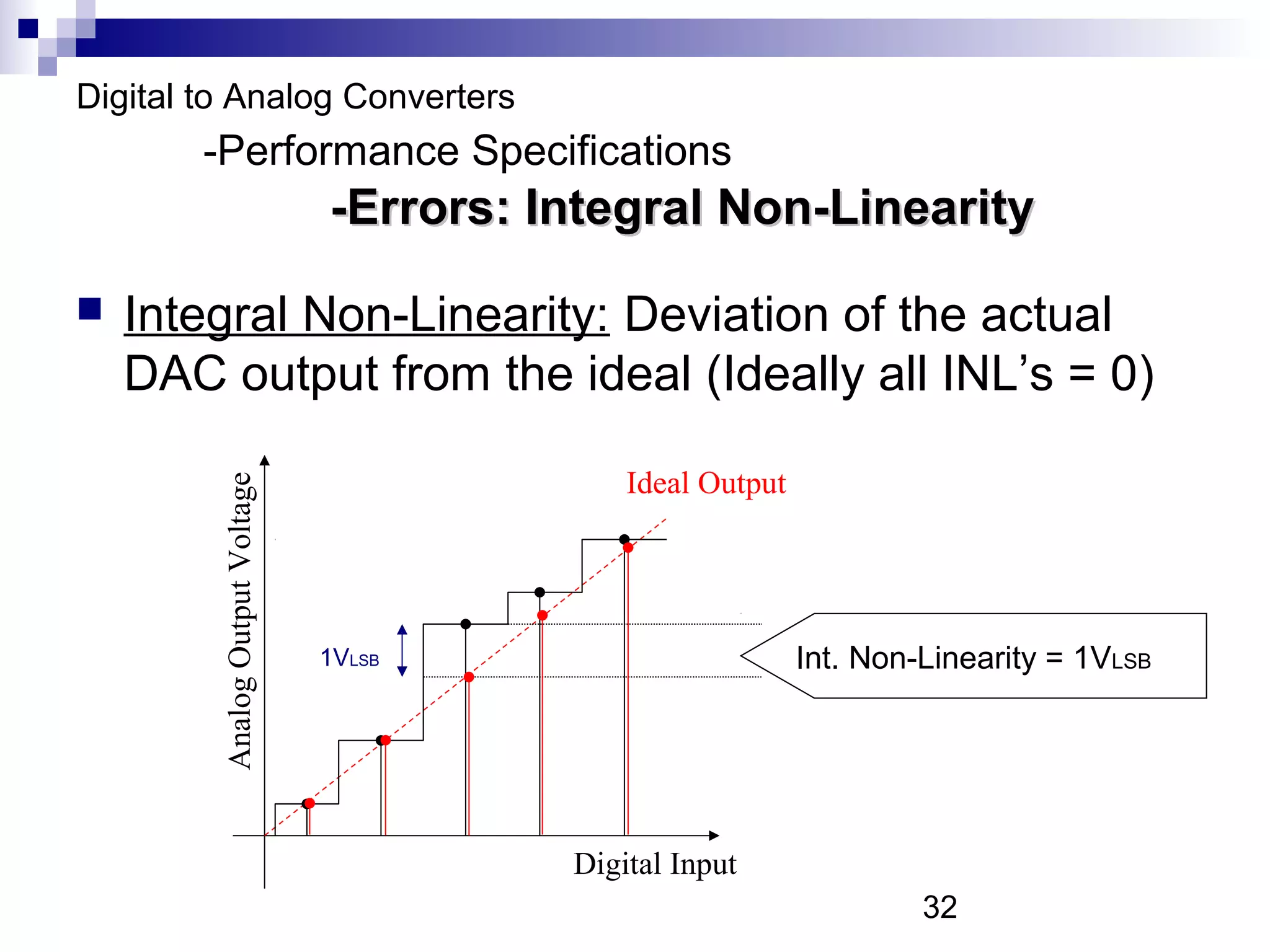
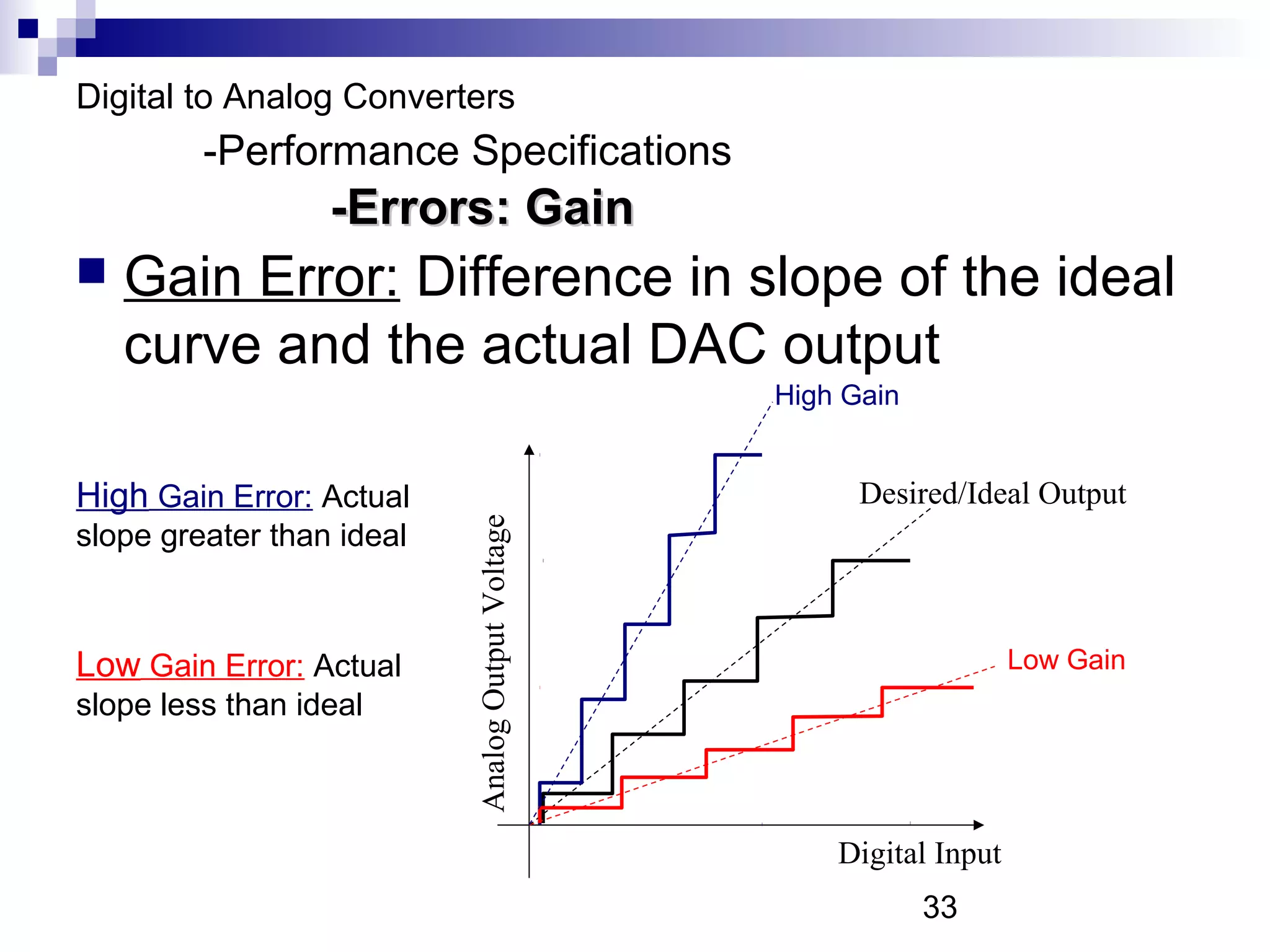
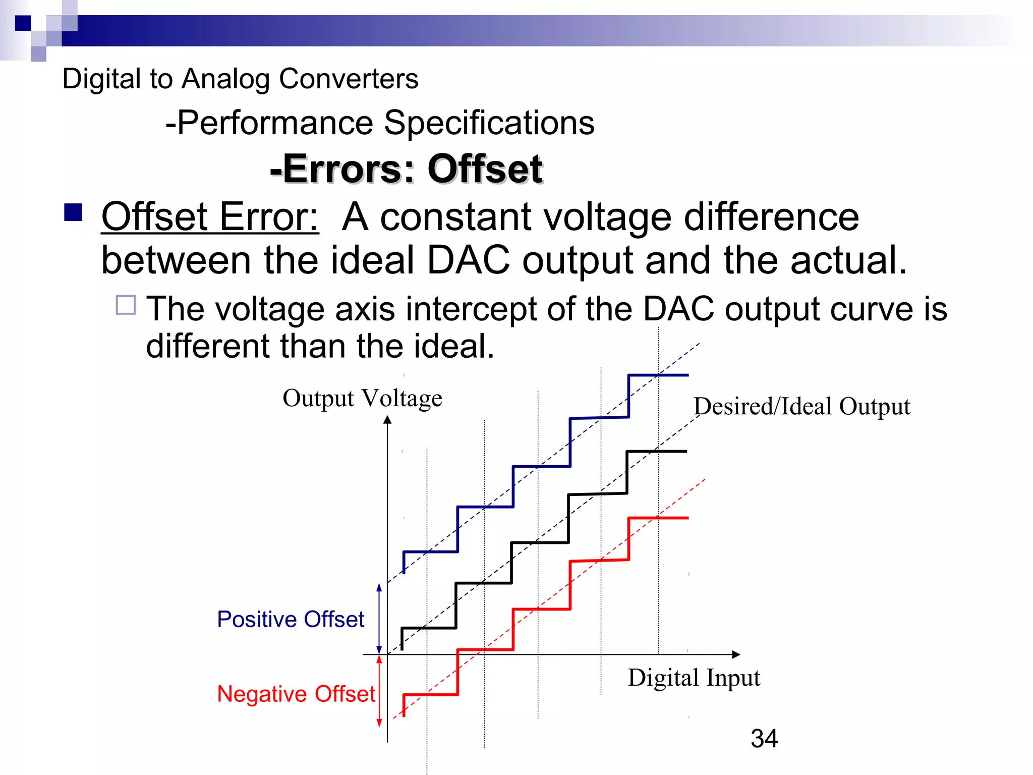
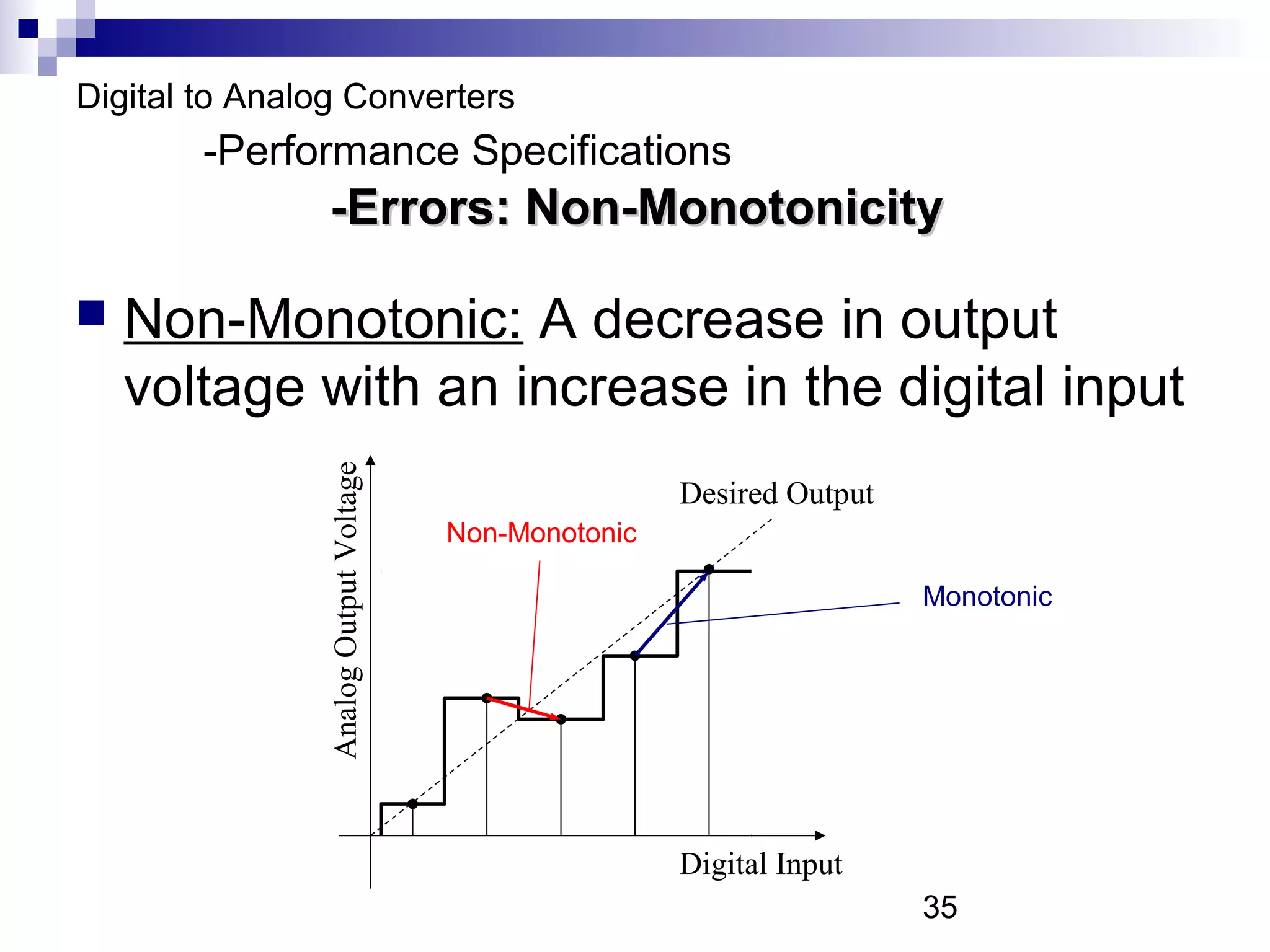
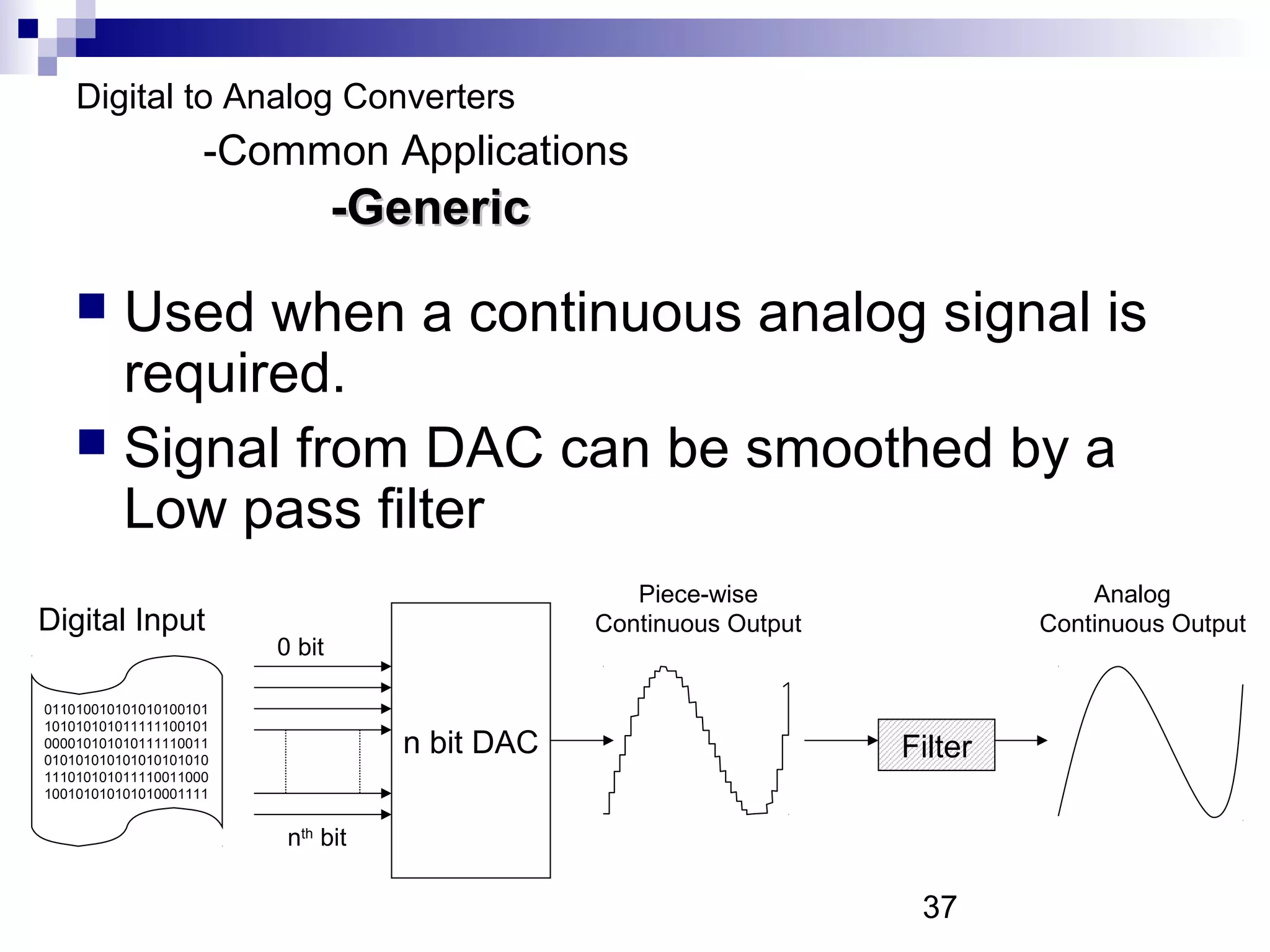
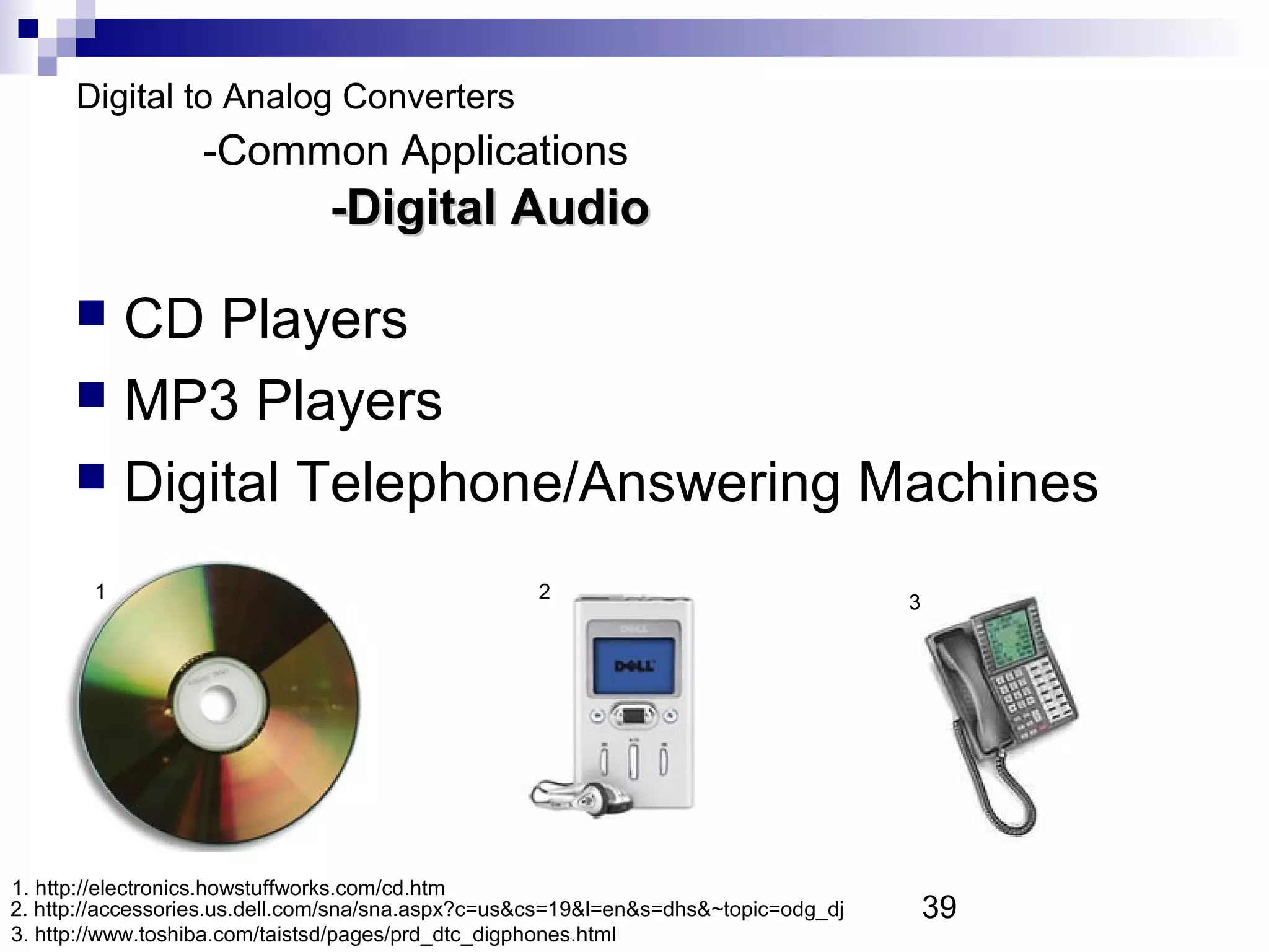
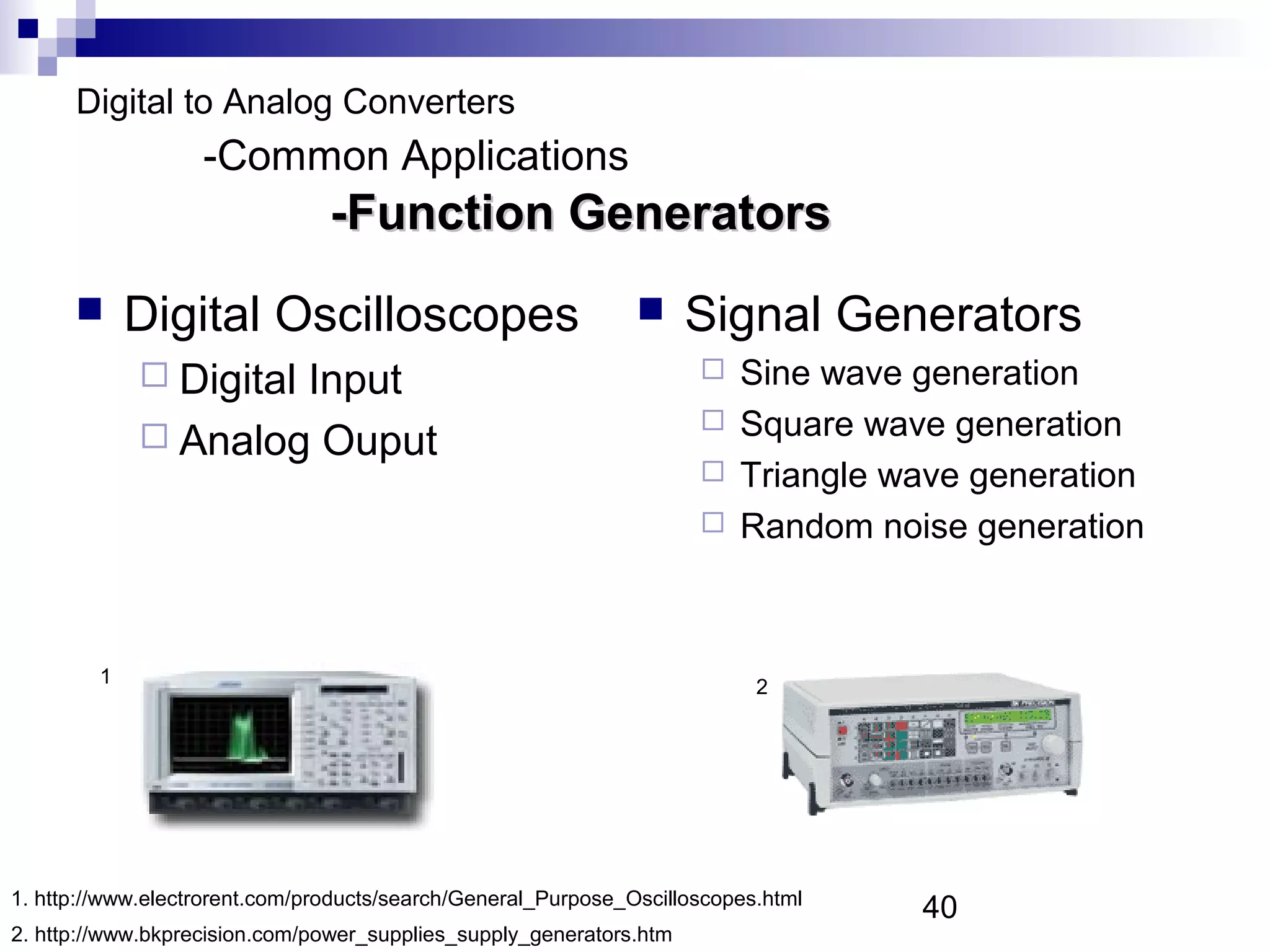
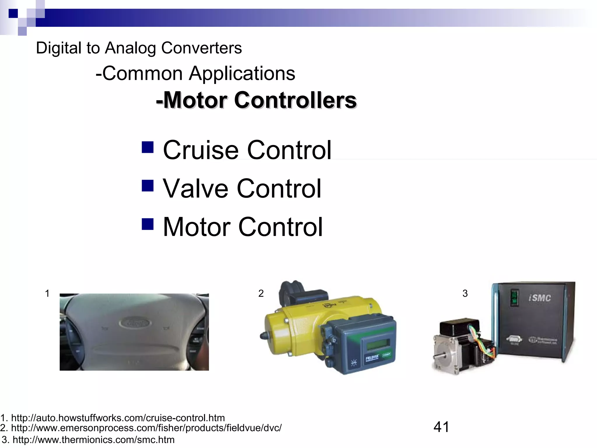
Digital to Analog
Converters (DAC)
   Adam Fleming
   Mark Hunkele
     3/11/2005
Outline
 Purpose
 Types
 Performance Characteristics
 Applications


                                2
Purpose
   To convert digital values to analog voltages
   Performs inverse operation of the Analog-to-
    Digital Converter (ADC)

    VOUT ∝ Digital Value

                    Reference Voltage


    Digital Value        DAC            Analog Voltage


                                        3
DACs
   Types
     Binary Weighted Resistor
     R-2R Ladder
     Multiplier DAC
          The reference voltage is constant and is set by the manufacturer.
     Non-Multiplier      DAC
          The reference voltage can be changed during operation.
   Characteristics
     Comprised   of switches, op-amps, and resistors
     Provides resistance inversely proportion to
      significance of bit

                                                            4
Binary Weighted Resistor
                                     Rf = R

                            ∑I   i


         R   2R   4R   8R                     Vo
   MSB


                                     LSB

-VREF

                                       5
Binary Representation
                                              Rf = R

                                     ∑I   i


                  R   2R   4R   8R                              Vo
Most
Significant Bit


                                              Least
                                              Significant Bit
       -VREF

                                                6
Binary Representation
                            SET       CLEARED
Most
Significant Bit


                                                Least
  -VREF                                         Significant Bit


                  ( 1   1         1    1 )2 = ( 15 )10


                                            7
Binary Weighted Resistor
   “Weighted                                             Rf = R
    Resistors”
    based on bit                                 ∑I   i

   Reduces
    current by a              R   2R   4R   8R                     Vo
    factor of 2 for     MSB
    each bit
                                                          LSB

                      -VREF

                                                 8
Binary Weighted Resistor
   Result:
                         B3 B2 B1 B0 
             ∑ I = VREF  R + 2R + 4 R + 8R 
                                           
                                      B2 B1 B0 
      VOUT     = I ⋅ R f = VREF  B3 +   + + 
                                      2  4  8 
     Bi =   Value of Bit i


                                            9
Binary Weighted Resistor
   More Generally:
                               Bi
             VOUT = VREF ∑     n −i −1
                               2
                    = VREF ⋅ Digital Value ⋅ Resolution
     Bi =   Value of Bit i
    n   = Number of Bits


                                             10
R-2R Ladder
VREF
         MSB


       LSB


                             11
R-2R Ladder
 Same input switch setup as Binary
  Weighted Resistor DAC
 All bits pass through resistance of 2R

          VREF
    MSB


    LSB

                                  12
R-2R Ladder
   The less significant the bit, the more resistors the signal
    muss pass through before reaching the op-amp
   The current is divided by a factor of 2 at each node

                LSB           MSB


                                                 13
R-2R Ladder
   The current is divided by a factor of 2 at each node
   Analysis for current from (001)2 shown below
                      I0        I0          I0
                      2         4           8
              R            R         R           2R
     R                2R        2R          2R

                 I0
                                                      Op-Amp input
            VREF
                           B1        B2               “Ground”

                                   − VREF      VREF
            B0             I0 =              =
                                2 R + 2 R 2 R 14 R
                                                3
R-2R Ladder
   Result:     VREF  B2 B1 B0 
             I=       + + 
                 3R  2      4   8 
                Rf       B2 B1 B0 
         VOUT =    VREF  + + 
                R        2    4   8 
     Bi =   Value of Bit i
                                     Rf


                                          15
R-2R Ladder
   If Rf = 6R, VOUT is same as Binary Weighted:
                          VREF      Bi
                       I=
                           3R
                                 ∑ 2 n −i
                                          Bi
                   VOUT = VREF ∑          n −i −1
                                      2
     Bi =   Value of Bit i


                                                    16
R-2R Ladder
       Example:                                − VREF         VREF
                                        I0 =                 =         = −1.67 mA
          Input = (101)2                    2 R + 2 R 2 R 3R
          VREF = 10 V                                       I0 I0
                                                 I op − amp = + = −1.04 mA
         R=2Ω                                               8 2
          Rf = 2R                                 VOUT = − I op − amp R f = 4.17 V

          R          R            R            2R
R               2R          2R            2R
           I0                      I0
                                               Op-Amp input
         VREF                    VREF
                                               “Ground”
          B0                     B2
                                                              17
Pros & Cons
         Binary Weighted                  R-2R
                              Only 2 resistor values
                              Easier implementation
Pros   Easily understood
                              Easier to manufacture
                              Faster response time

       Limited to ~ 8 bits
       Large # of resistors
Cons   Susceptible to noise   More confusing analysis
       Expensive
       Greater Error
                                            18
Digital to Analog Converters


  Performance   Specifications

  Common   Applications


         Presented by: Mark Hunkele
                                      19
Digital to Analog Converters
      -Performance Specifications

           Resolution
           Reference Voltages
           Settling Time
           Linearity
           Speed
           Errors


                                    20
Digital to Analog Converters
        -Performance Specifications
                -Resolution

 Resolution: is the amount of variance in
  output voltage for every change of the LSB
  in the digital input.
 How closely can we approximate the
  desired output signal(Higher Res. = finer
  detail=smaller Voltage divisions)
 A common DAC has a 8 - 12 bit Resolution

                                 VRef
            Resolution = VLSB   = N     N = Number of bits
                                  2        21
Digital to Analog Converters
                        -Performance Specifications
                              -Resolution

                 Poor Resolution(1 bit)                                       Better Resolution(3 bit)

         Vout                                                    Vout
                                 Desired Analog                                                               Desired Analog signal
                                 signal
                                                                                                        111

                                                                                                  110          110


                                                       8 Volt. Levels
2 Volt. Levels


                             1
                                                                                            101                      101

                                                                                          100                              100

                                                                                    011                                          011

                                                                                010                                                    010

                                                                              001                                                            001

                    0                     0                             000
                                                                                                                                                   000

                                       Digital Input                                Approximate                            Digital Input
                   Approximate
                                                                                    output 22
                   output
Digital to Analog Converters
        -Performance Specifications
                -Reference Voltage

 Reference Voltage: A specified voltage
  used to determine how each digital input
  will be assigned to each voltage division.
 Types:
     Non-multiplier:      internal, fixed, and defined by
      manufacturer
     Multiplier: external, variable, user specified


                                              23
Digital to Analog Converters
           -Performance Specifications
                     -Reference Voltage


      Non-Multiplier: (Vref = C)                              Multiplier: (Vref = Asin(wt))
 Voltage                                       Voltage
3C                                                                   11
                                               3A
 4
                     11                         4
 C                                              A               10         10
 2              10        10                    2
 C                                              A        01                     01
 4         01                  01               4

  0                                             0
      00                             00             00                                00
                               Digital Input                                         Digital Input


                                    Assume 2 bit DAC                 24
Digital to Analog Converters
        -Performance Specifications
                -Settling Time

 Settling Time: The time required for the
  input signal voltage to settle to the
  expected output voltage(within +/- V LSB).
 Any change in the input state will not be
  reflected in the output state immediately.
  There is a time lag, between the two
  events.

                                      25
Digital to Analog Converters
           -Performance Specifications
                    -Settling Time

      Analog Output Voltage


            +VLSB
Expected
Voltage     -VLSB


                                               Time
                          Settling time
                                          26
Digital to Analog Converters
        -Performance Specifications
                -Linearity

 Linearity: is the difference between the desired
  analog output and the actual output over the
  full range of expected values.
 Ideally, a DAC should produce a linear
  relationship between a digital input and the
  analog output, this is not always the case.


                                      27
Digital to Analog Converters
                                -Performance Specifications
                                        -Linearity

                        Linearity(Ideal Case)                                      NON-Linearity(Real World)


                                                               Analog Output Voltage
Analog Output Voltage


                                  Desired/Approximate Output                                         Desired Output


                                                                                                       Approximate
                                                                                                       output


                                            Digital Input                                            Digital Input

                          Perfect Agreement                                            Miss-alignment
                                                                                                28
Digital to Analog Converters
        -Performance Specifications
                -Speed

 Speed: Rate of conversion of a single
  digital input to its analog equivalent
 Conversion Rate
     Depends on clock speed of input signal
     Depends on settling time of converter


                                      29
Digital to Analog Converters
        -Performance Specifications
                -Errors

   Non-linearity
     Differential
     Integral
 Gain
 Offset
 Non-monotonicity


                                      30
Digital to Analog Converters
        -Performance Specifications
                                         -Errors: Differential Non-Linearity
   Differential Non-Linearity: Difference in voltage step size
    from the previous DAC output (Ideally All DLN’s = 1
    VLSB)
          Analog Output Voltage


                                                     Ideal Output


                                          2VLSB              Diff. Non-Linearity = 2VLSB

                                  VLSB


                                                    Digital Input           31
Digital to Analog Converters
        -Performance Specifications
                                 -Errors: Integral Non-Linearity
   Integral Non-Linearity: Deviation of the actual
    DAC output from the ideal (Ideally all INL’s = 0)

                                               Ideal Output
         Analog Output Voltage


                                 1VLSB                        Int. Non-Linearity = 1VLSB


                                           Digital Input
                                                                       32
Digital to Analog Converters
         -Performance Specifications
                  -Errors: Gain
   Gain Error: Difference in slope of the ideal
    curve and the actual DAC output
                                                   High Gain


High Gain Error: Actual    Analog Output Voltage         Desired/Ideal Output
slope greater than ideal


Low Gain Error: Actual                                                 Low Gain
slope less than ideal


                                                       Digital Input
                                                               33
Digital to Analog Converters
        -Performance Specifications
              -Errors: Offset
   Offset Error: A constant voltage difference
    between the ideal DAC output and the actual.
     The  voltage axis intercept of the DAC output curve is
      different than the ideal.
                  Output Voltage            Desired/Ideal Output


            Positive Offset

                                      Digital Input
            Negative Offset
                                                  34
Digital to Analog Converters
        -Performance Specifications
                 -Errors: Non-Monotonicity

   Non-Monotonic: A decrease in output
    voltage with an increase in the digital input
                Analog Output Voltage


                                                        Desired Output
                                        Non-Monotonic

                                                                         Monotonic


                                                        Digital Input
                                                                         35
Digital to Analog Converters
      -Common Applications


  Generic use
  Circuit Components
  Digital Audio
  Function Generators/Oscilloscopes
  Motor Controllers


                               36
Digital to Analog Converters
                    -Common Applications
                                -Generic
     Used when a continuous analog signal is
      required.
     Signal from DAC can be smoothed by a
      Low pass filter
                                                  Piece-wise                    Analog
Digital Input                                  Continuous Output            Continuous Output
                        0 bit

011010010101010100101
101010101011111100101
000010101010111110011
010101010101010101010
                                   n bit DAC                       Filter
111010101011110011000
100101010101010001111


                         nth bit

                                                                    37
Digital to Analog Converters
        -Common Applications
                  -Circuit Components
   Voltage controlled Amplifier
     digital   input, External Reference Voltage as control


   Digitally operated attenuator
     External    Reference Voltage as input, digital control


   Programmable Filters
     Digitally   controlled cutoff frequencies

                                                  38
Digital to Analog Converters
                  -Common Applications
                               -Digital Audio

       CD Players
       MP3 Players
       Digital Telephone/Answering Machines

        1                                          2                                 3


1. http://electronics.howstuffworks.com/cd.htm
2. http://accessories.us.dell.com/sna/sna.aspx?c=us&cs=19&l=en&s=dhs&~topic=odg_dj       39
3. http://www.toshiba.com/taistsd/pages/prd_dtc_digphones.html
Digital to Analog Converters
                   -Common Applications
                                -Function Generators
            Digital Oscilloscopes                                  Signal Generators
              Digital
                     Input                                            Sine wave generation
                                                                      Square wave generation
              Analog Ouput
                                                                      Triangle wave generation
                                                                      Random noise generation


         1                                                                 2


1. http://www.electrorent.com/products/search/General_Purpose_Oscilloscopes.html
                                                                                   40
2. http://www.bkprecision.com/power_supplies_supply_generators.htm
Digital to Analog Converters
                    -Common Applications
                                  -Motor Controllers

                               Cruise Control
                               Valve Control
                               Motor Control


         1                                              2             3


1. http://auto.howstuffworks.com/cruise-control.htm
2. http://www.emersonprocess.com/fisher/products/fieldvue/dvc/   41
3. http://www.thermionics.com/smc.htm
References
   Cogdell, J.R. Foundations of Electrical Engineering. 2nd ed. Upper Saddle River, NJ:
    Prentice Hall, 1996.
   “Simplified DAC/ADC Lecture Notes,” http://www-personal.engin.umd.umich.edu/
    ~fmeral/ELECTRONICS II/ElectronicII.html
   “Digital-Analog Conversion,” http://www.allaboutcircuits.com.
   Barton, Kim, and Neel. “Digital to Analog Converters.” Lecture, March 21, 2001.
    http://www.me.gatech.edu/charles.ume/me4447Spring01/ClassNotes/dac.ppt.

   Chacko, Deliou, Holst, “ME6465 DAC Lecture” Lecture, 10/ 23/2003,
    http://www.me.gatech.edu/mechatronics_course/
   Lee, Jeelani, Beckwith, “Digital to Analog Converter” Lecture, Spring 2004,
    http://www.me.gatech.edu/mechatronics_course/


                                                                   42

Dac s05

  • 1.
    Digital to Analog Converters(DAC) Adam Fleming Mark Hunkele 3/11/2005
  • 2.
    Outline  Purpose  Types Performance Characteristics  Applications 2
  • 3.
    Purpose  To convert digital values to analog voltages  Performs inverse operation of the Analog-to- Digital Converter (ADC)  VOUT ∝ Digital Value Reference Voltage Digital Value DAC Analog Voltage 3
  • 4.
    DACs  Types  Binary Weighted Resistor  R-2R Ladder  Multiplier DAC  The reference voltage is constant and is set by the manufacturer.  Non-Multiplier DAC  The reference voltage can be changed during operation.  Characteristics  Comprised of switches, op-amps, and resistors  Provides resistance inversely proportion to significance of bit 4
  • 5.
    Binary Weighted Resistor Rf = R ∑I i R 2R 4R 8R Vo MSB LSB -VREF 5
  • 6.
    Binary Representation Rf = R ∑I i R 2R 4R 8R Vo Most Significant Bit Least Significant Bit -VREF 6
  • 7.
    Binary Representation SET CLEARED Most Significant Bit Least -VREF Significant Bit ( 1 1 1 1 )2 = ( 15 )10 7
  • 8.
    Binary Weighted Resistor  “Weighted Rf = R Resistors” based on bit ∑I i  Reduces current by a R 2R 4R 8R Vo factor of 2 for MSB each bit LSB -VREF 8
  • 9.
    Binary Weighted Resistor  Result:  B3 B2 B1 B0  ∑ I = VREF  R + 2R + 4 R + 8R     B2 B1 B0  VOUT = I ⋅ R f = VREF  B3 + + +   2 4 8   Bi = Value of Bit i 9
  • 10.
    Binary Weighted Resistor  More Generally: Bi VOUT = VREF ∑ n −i −1 2 = VREF ⋅ Digital Value ⋅ Resolution  Bi = Value of Bit i n = Number of Bits 10
  • 11.
  • 12.
    R-2R Ladder  Sameinput switch setup as Binary Weighted Resistor DAC  All bits pass through resistance of 2R VREF MSB LSB 12
  • 13.
    R-2R Ladder  The less significant the bit, the more resistors the signal muss pass through before reaching the op-amp  The current is divided by a factor of 2 at each node LSB MSB 13
  • 14.
    R-2R Ladder  The current is divided by a factor of 2 at each node  Analysis for current from (001)2 shown below I0 I0 I0 2 4 8 R R R 2R R 2R 2R 2R I0 Op-Amp input VREF B1 B2 “Ground” − VREF VREF B0 I0 = = 2 R + 2 R 2 R 14 R 3
  • 15.
    R-2R Ladder  Result: VREF  B2 B1 B0  I=  + +  3R  2 4 8  Rf  B2 B1 B0  VOUT = VREF  + +  R  2 4 8   Bi = Value of Bit i Rf 15
  • 16.
    R-2R Ladder  If Rf = 6R, VOUT is same as Binary Weighted: VREF Bi I= 3R ∑ 2 n −i Bi VOUT = VREF ∑ n −i −1 2  Bi = Value of Bit i 16
  • 17.
    R-2R Ladder  Example: − VREF VREF I0 = = = −1.67 mA  Input = (101)2 2 R + 2 R 2 R 3R  VREF = 10 V I0 I0 I op − amp = + = −1.04 mA R=2Ω 8 2  Rf = 2R VOUT = − I op − amp R f = 4.17 V R R R 2R R 2R 2R 2R I0 I0 Op-Amp input VREF VREF “Ground” B0 B2 17
  • 18.
    Pros & Cons Binary Weighted R-2R Only 2 resistor values Easier implementation Pros Easily understood Easier to manufacture Faster response time Limited to ~ 8 bits Large # of resistors Cons Susceptible to noise More confusing analysis Expensive Greater Error 18
  • 19.
    Digital to AnalogConverters  Performance Specifications  Common Applications Presented by: Mark Hunkele 19
  • 20.
    Digital to AnalogConverters -Performance Specifications  Resolution  Reference Voltages  Settling Time  Linearity  Speed  Errors 20
  • 21.
    Digital to AnalogConverters -Performance Specifications -Resolution  Resolution: is the amount of variance in output voltage for every change of the LSB in the digital input.  How closely can we approximate the desired output signal(Higher Res. = finer detail=smaller Voltage divisions)  A common DAC has a 8 - 12 bit Resolution VRef Resolution = VLSB = N N = Number of bits 2 21
  • 22.
    Digital to AnalogConverters -Performance Specifications -Resolution Poor Resolution(1 bit) Better Resolution(3 bit) Vout Vout Desired Analog Desired Analog signal signal 111 110 110 8 Volt. Levels 2 Volt. Levels 1 101 101 100 100 011 011 010 010 001 001 0 0 000 000 Digital Input Approximate Digital Input Approximate output 22 output
  • 23.
    Digital to AnalogConverters -Performance Specifications -Reference Voltage  Reference Voltage: A specified voltage used to determine how each digital input will be assigned to each voltage division.  Types:  Non-multiplier: internal, fixed, and defined by manufacturer  Multiplier: external, variable, user specified 23
  • 24.
    Digital to AnalogConverters -Performance Specifications -Reference Voltage Non-Multiplier: (Vref = C) Multiplier: (Vref = Asin(wt)) Voltage Voltage 3C 11 3A 4 11 4 C A 10 10 2 10 10 2 C A 01 01 4 01 01 4 0 0 00 00 00 00 Digital Input Digital Input Assume 2 bit DAC 24
  • 25.
    Digital to AnalogConverters -Performance Specifications -Settling Time  Settling Time: The time required for the input signal voltage to settle to the expected output voltage(within +/- V LSB).  Any change in the input state will not be reflected in the output state immediately. There is a time lag, between the two events. 25
  • 26.
    Digital to AnalogConverters -Performance Specifications -Settling Time Analog Output Voltage +VLSB Expected Voltage -VLSB Time Settling time 26
  • 27.
    Digital to AnalogConverters -Performance Specifications -Linearity  Linearity: is the difference between the desired analog output and the actual output over the full range of expected values.  Ideally, a DAC should produce a linear relationship between a digital input and the analog output, this is not always the case. 27
  • 28.
    Digital to AnalogConverters -Performance Specifications -Linearity Linearity(Ideal Case) NON-Linearity(Real World) Analog Output Voltage Analog Output Voltage Desired/Approximate Output Desired Output Approximate output Digital Input Digital Input Perfect Agreement Miss-alignment 28
  • 29.
    Digital to AnalogConverters -Performance Specifications -Speed  Speed: Rate of conversion of a single digital input to its analog equivalent  Conversion Rate  Depends on clock speed of input signal  Depends on settling time of converter 29
  • 30.
    Digital to AnalogConverters -Performance Specifications -Errors  Non-linearity  Differential  Integral  Gain  Offset  Non-monotonicity 30
  • 31.
    Digital to AnalogConverters -Performance Specifications -Errors: Differential Non-Linearity  Differential Non-Linearity: Difference in voltage step size from the previous DAC output (Ideally All DLN’s = 1 VLSB) Analog Output Voltage Ideal Output 2VLSB Diff. Non-Linearity = 2VLSB VLSB Digital Input 31
  • 32.
    Digital to AnalogConverters -Performance Specifications -Errors: Integral Non-Linearity  Integral Non-Linearity: Deviation of the actual DAC output from the ideal (Ideally all INL’s = 0) Ideal Output Analog Output Voltage 1VLSB Int. Non-Linearity = 1VLSB Digital Input 32
  • 33.
    Digital to AnalogConverters -Performance Specifications -Errors: Gain  Gain Error: Difference in slope of the ideal curve and the actual DAC output High Gain High Gain Error: Actual Analog Output Voltage Desired/Ideal Output slope greater than ideal Low Gain Error: Actual Low Gain slope less than ideal Digital Input 33
  • 34.
    Digital to AnalogConverters -Performance Specifications -Errors: Offset  Offset Error: A constant voltage difference between the ideal DAC output and the actual.  The voltage axis intercept of the DAC output curve is different than the ideal. Output Voltage Desired/Ideal Output Positive Offset Digital Input Negative Offset 34
  • 35.
    Digital to AnalogConverters -Performance Specifications -Errors: Non-Monotonicity  Non-Monotonic: A decrease in output voltage with an increase in the digital input Analog Output Voltage Desired Output Non-Monotonic Monotonic Digital Input 35
  • 36.
    Digital to AnalogConverters -Common Applications  Generic use  Circuit Components  Digital Audio  Function Generators/Oscilloscopes  Motor Controllers 36
  • 37.
    Digital to AnalogConverters -Common Applications -Generic  Used when a continuous analog signal is required.  Signal from DAC can be smoothed by a Low pass filter Piece-wise Analog Digital Input Continuous Output Continuous Output 0 bit 011010010101010100101 101010101011111100101 000010101010111110011 010101010101010101010 n bit DAC Filter 111010101011110011000 100101010101010001111 nth bit 37
  • 38.
    Digital to AnalogConverters -Common Applications -Circuit Components  Voltage controlled Amplifier  digital input, External Reference Voltage as control  Digitally operated attenuator  External Reference Voltage as input, digital control  Programmable Filters  Digitally controlled cutoff frequencies 38
  • 39.
    Digital to AnalogConverters -Common Applications -Digital Audio  CD Players  MP3 Players  Digital Telephone/Answering Machines 1 2 3 1. http://electronics.howstuffworks.com/cd.htm 2. http://accessories.us.dell.com/sna/sna.aspx?c=us&cs=19&l=en&s=dhs&~topic=odg_dj 39 3. http://www.toshiba.com/taistsd/pages/prd_dtc_digphones.html
  • 40.
    Digital to AnalogConverters -Common Applications -Function Generators  Digital Oscilloscopes  Signal Generators  Digital Input  Sine wave generation  Square wave generation  Analog Ouput  Triangle wave generation  Random noise generation 1 2 1. http://www.electrorent.com/products/search/General_Purpose_Oscilloscopes.html 40 2. http://www.bkprecision.com/power_supplies_supply_generators.htm
  • 41.
    Digital to AnalogConverters -Common Applications -Motor Controllers  Cruise Control  Valve Control  Motor Control 1 2 3 1. http://auto.howstuffworks.com/cruise-control.htm 2. http://www.emersonprocess.com/fisher/products/fieldvue/dvc/ 41 3. http://www.thermionics.com/smc.htm
  • 42.
    References  Cogdell, J.R. Foundations of Electrical Engineering. 2nd ed. Upper Saddle River, NJ: Prentice Hall, 1996.  “Simplified DAC/ADC Lecture Notes,” http://www-personal.engin.umd.umich.edu/ ~fmeral/ELECTRONICS II/ElectronicII.html  “Digital-Analog Conversion,” http://www.allaboutcircuits.com.  Barton, Kim, and Neel. “Digital to Analog Converters.” Lecture, March 21, 2001. http://www.me.gatech.edu/charles.ume/me4447Spring01/ClassNotes/dac.ppt.  Chacko, Deliou, Holst, “ME6465 DAC Lecture” Lecture, 10/ 23/2003, http://www.me.gatech.edu/mechatronics_course/  Lee, Jeelani, Beckwith, “Digital to Analog Converter” Lecture, Spring 2004, http://www.me.gatech.edu/mechatronics_course/ 42