Download to read offline
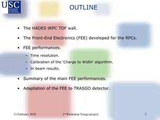
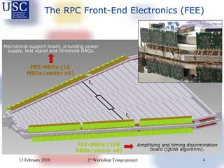
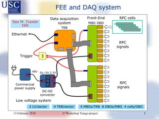
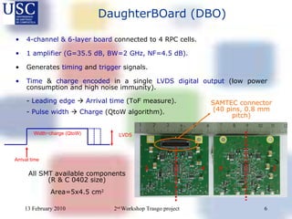
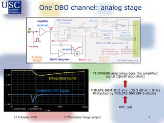
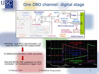
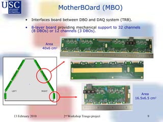
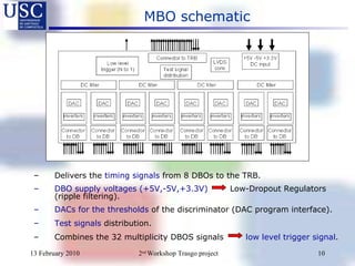
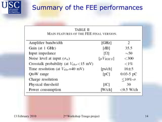
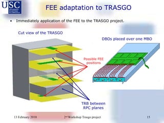
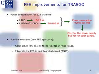


The document discusses the front-end electronics (FEE) developed for the timing RPCs used in the HADES experiment. The FEE consists of daughter boards (DBOs) connected to the RPC cells that amplify and digitize signals, and mother boards (MBOs) that interface between the DBOs and data acquisition system. The FEE achieves a time resolution of less than 17 ps using a charge-to-width algorithm to encode timing and charge information. Testing shows the FEE performs well and could be adapted for use in the TRASGO detector with some modifications to reduce power consumption.


![RF Module Design - [Chapter 4] Transceiver Architecture](https://cdn.slidesharecdn.com/ss_thumbnails/rfch4-150613070346-lva1-app6891-thumbnail.jpg?width=640&height=640&fit=bounds)