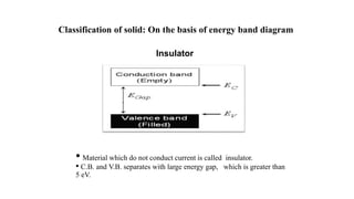
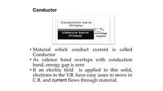
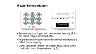
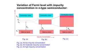
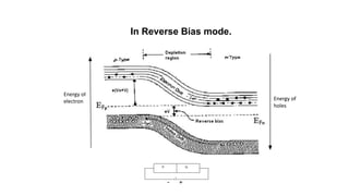
1. Classification of solid: On the basis of energy band diagram
• Material which do not conduct current is called insulator.
• C.B. and V.B. separates with large energy gap, which is greater than
5 eV.
Insulator
2. Semiconductor
• Materials which have conductivity lies between
insulator and conductor are called
Semiconductor.
• Energy gap is small and it is of the order of 1eV.
3. Conductor
• Material which conduct current is called
Conductor
• As valence band overlaps with conduction
band, energy gap is zero
• If an electric field is applied to this solid,
electrons in the V.B. have easy asses to move in
C.B. and current flows through material.
4. Types of Semiconductor
• Intrinsic Semiconductor: Chemically pure
semiconductor is called Intrinsic Semiconductor.
• Extrinsic Semiconductor: Semiconductor doped
with some external impurity are called Extrinsic
semiconductor.
• Doping: It is the Process of adding impurities into
an intrinsic semiconductor .
6. N-type Semiconductor:
Two dimensional representation The Band Structure View
• Semiconductors doped with pentavalent impurity (P,As)
are called N-type semiconductor.
• As pentavalent impurity atom donate free electrons it is
called Donor impurity.
• Donor impurities “create” an energy level, close to the
conduction band & represented by ED .
7. P-type Semiconductor:
Two dimensional representation The Band Structure View
• Semiconductors doped with trivalent impurity (Al, B) are
called P-type semiconductor.
• As trivalent impurity accept free electrons, so we call them
Acceptors.
• Acceptor impurities “create” discrete energy level, close to
the valence band & represented by EA .
8. Concept of Holes:
• Hole is nothing but the absence of electron.
• “Deficiency” of negative charge can be treated as a
positive charge.
• Holes are positive charge carriers. Movement of electrons
from nearby sites gives rise to movement of holes in
apposite direction.
• Hole is just like a bubble in liquid.
9. Fermi level & Fermi Energy
• For conductor: The highest occupied energy level at
0ok is called Fermi level and the Energy
corresponding to it is called the Fermi Energy.
• For semiconductor: Fermi level is the reference
energy level and it correspond to the center of
gravity of conduction electron and valence hole.
10. Fermi-Dirac Distribution Function
)
exp(
1
1
)
(
kT
E
E
E
f
F
• f(E) is the function that gives the probability that particular
energy level having energy E is occupied by an electron at
Temperature T0 Kelvin. Where EF is the Fermi energy, k is
Boltzmann's constant.
• For conductor: The highest occupied energy level at 0K is called
Fermi level and the Energy corresponding to it is called the Fermi
Energy.
• For semiconductor: Fermi level is the reference energy level and
it correspond to the center of gravity of conduction electron and
valence hole.
11. Effect of temperature on Fermi Function
The above diagram represents variation of f(E) as a function of temperature.
All the curves pass through cross-over point C corresponding to f(E) =1/2.
12. Fermi level in Intrinsic semiconductor
• At T=0K the number of electrons in conduction band equals
the number of holes in valence band, ne = nh = ni .
Fermi level lies in the middle of the band gap.
• At T≠ 0 K, it depends upon the effective mass of electron and
hole.
*
*
g
ln
4
3
2 h
e
f
m
m
kT
E
E
m*h>m*e
Temperature
Energy
Valence band
Conduction band
m*h = m*e
m*h < m*e
13. Fermi level in p-type semiconductor
• The number of holes in valence band are greater than
number of electrons in conduction band, nh > ne
• So the Fermi level shift towards the valence band.
• With temperature fermi level shifts towards Efi .,
Energy Band Diagram of n-type semiconductor at 0K and 300K
14. Fermi level in n-type semiconductor
• The number of electrons in conduction band are greater
than number of holes in valence band, ne > nh
• So the Fermi level shift towards the conduction band .
• With temperature Fermi level shifts towards the EFi
Energy Band Diagram of p-type semiconductor at 0K and 300K
15. Variation of Fermi level with impurity
concentration in n-type semiconductor:
Fig. (a): At low impurity concentration
Fig. (b): At moderate impurity concentration
Fig. (c): At high impurity concentration
Eg
Eg
Eg
Conduction band Conduction band
Valence band Valence band Valence band
ED
EF
EC
EV
E
Impurity Concentration
Fig: (a) Fig: (b) Fig: (c)
Eg
Conduction band
16. Drift Current
Drift current: The current due to (motion) drifting of
charge carrier under application of electric field is
called Drift Current.
Drift current density is given by
Where are the constants called mobility
of electrons and holes respectively.
h
e
,
E
e
n
drift
e e
J
)
(
E
e
p
drift
h h
J
)
(
)
(
)
(
)
( drift
J
drift
J
drift h
e
J
17. Diffusion current
• Diffusion current: The directional movement of charge
carriers due to concentration gradient is called Diffusion
Current.
• Diffusion current density due to electron is given by
• Diffusion current density due to hole is given by
Where De and Dh are the diffusion coefficient for electron and
hole respectively.
dx
dn
e
diffusion
e D
e
J
)
(
dx
dp
h
diffusion
h D
e
J
)
(
)
(
)
(
)
( diffusion
J
diffusion
J
diffusion h
e
J
18. Conductivity of semiconductor
• Conductivity of intrinsic semiconductor:
σi = ni e( μe + μh)
• Conductivity of Extrinsic semiconductor:
For n – type semiconductor:
σn = n e μe = ND e μe
For p – type semiconductor:
σp = p e μh = NA e μh
Where ND and NA are the concentration of donor and
acceptor impurity.
19. p – n junction Diode
• The diode is just like a current valve.
• It allows unidirectional flow of current.
• Diode conduct only when it is in forward bias and do not
conduct ideally in reverse bias.
• It is used in rectifiers.
• Diode has a nonlinear voltage - current characteristics.
20. Formation of p-n Junction Diode
• Holes are the majority charge carriers and electrons are
the minority charge carriers in p- region.
• Electrons are the majority charge carriers and holes are
the minority charge carriers in n- region.
• p-n junction is the boundary between p-type and n-type
semiconductor.
22. Biasing of p-n junction diode
Biasing of diode: Terminals of external battery is
connected to the terminals of diode is called as
biasing of diode.
• Forward Biasing: p terminal of diode is
connected to +ve and n terminal is connected to –
ve terminal of battery.
• Reverse Biasing: n terminal of diode is
connected to +ve and p terminal is connected to –
ve terminal of battery.
28. Transistor = Trans + resistor
• The transistor can be thought as a device in which
current travels from low resistance to high resistance
path.
Bipolar Junction Transistor
29. 1. Common base mode
2. Common emitter mode
3. Common collector mode
• For efficient action of a transistor,
emitter- base junction is forward biased
and collector is reverse biased.
Modes of operation of Transistor
30. Energy band Diagram of a transistor
n-p-n Transistor in unbiased mode
Energy of
electrons
Energy of
holes
32. • When a current carrying conductor is placed in a
transverse magnetic field, a potential difference is
generated in the direction perpendicular to both the current
and the magnetic field, the voltage developed is known as
Hall voltage VH and the effect is known as Hall effect.
I
B
v
B
F
Lorentz Force
F= -eBVd
d
I
e
-
+
VH
-
The Hall Effect: Discovered in 1897 by Edwin
H. Hall
33. Current Flow in N-type Semiconductors
• The DC voltage source has a
positive terminal that attracts
the free electrons in the
semiconductor and pulls them
away from their atoms leaving
the atoms charged positively.
• Electrons from the negative
terminal of the supply enter
the semiconductor material
and are attracted by the
positive charge of the atoms
missing one of their electrons.
• Current (electrons) flows from
the positive terminal to the
negative terminal.
34. Current Flow in P-type Semiconductors
• Electrons from the negative
supply terminal are attracted to
the positive holes and fill them.
• The positive terminal of the
supply pulls the electrons from
the holes leaving the holes to
attract more electrons.
• Current (electrons) flows from
the negative terminal to the
positive terminal.
• Inside the semiconductor
current flow is actually by the
movement of the holes from
positive to negative.
35. Application of Hall Effect
• Determination of the “type of semiconductor”
• Determination of the “concentration” of charge
carrier (p or n).
• Determination of the “mobility” of charge carrier
(µ).
• Measurement of “magnetic field” (B).
• Measurement of “Hall coefficient” (RH).