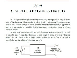
Downloaded 385 times


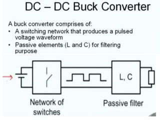
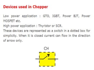
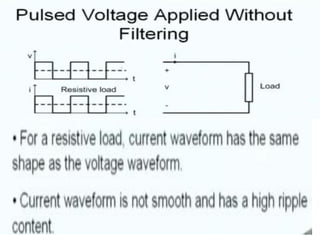
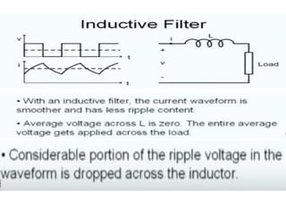


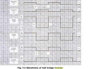
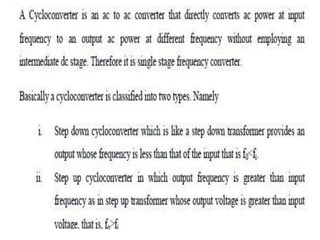
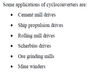


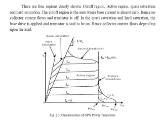
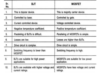
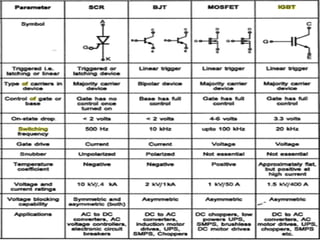
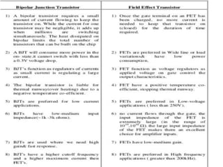
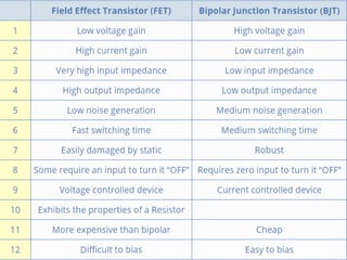

The document discusses various types of rectifier circuits including uncontrolled and controlled single phase and three phase rectifiers. It also discusses different power electronic converters such as inverters, choppers, and cycloconverters. Key devices for power electronics applications discussed include transistors, MOSFETs, IGBTs, and thyristors. Application areas mentioned include UPS, HVDC transmission, and motor drives. The document provides circuit diagrams, operating principles, and example calculations for different power electronic converters.


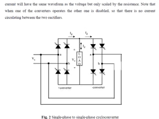
![[Daniel_W._Hart]_Power_Electronic(www.knowing.ir)-1 (1).pdf](https://cdn.slidesharecdn.com/ss_thumbnails/danielw-231119080747-193d829a-thumbnail.jpg?width=640&height=640&fit=bounds)