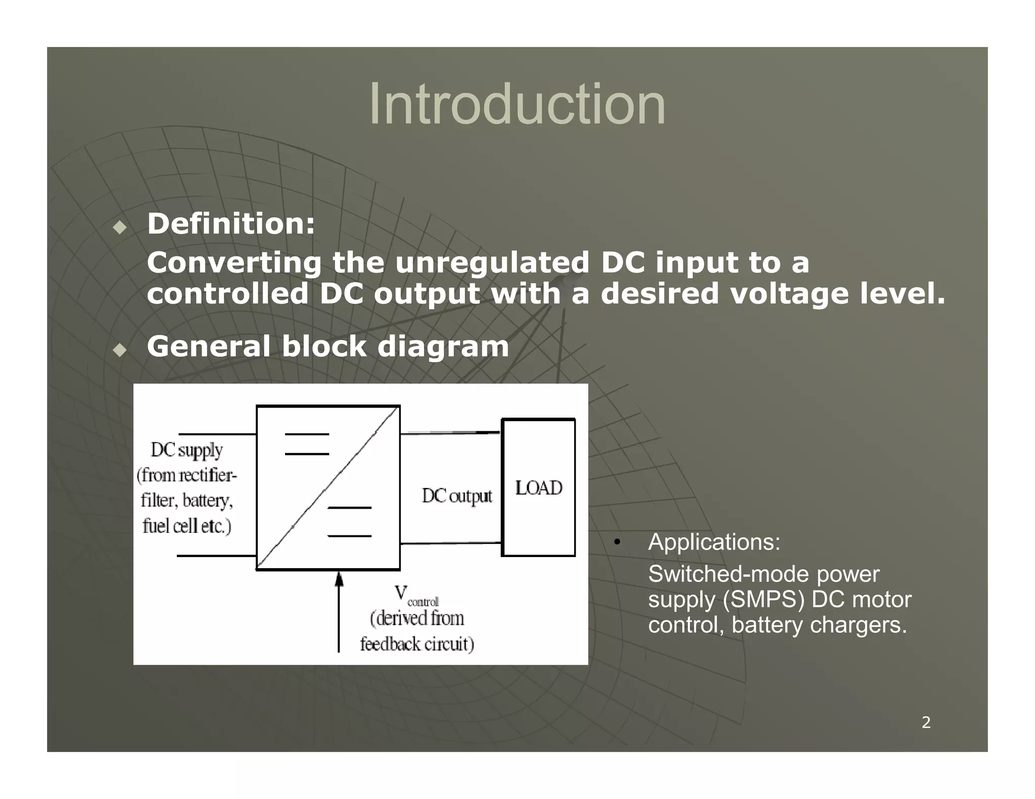
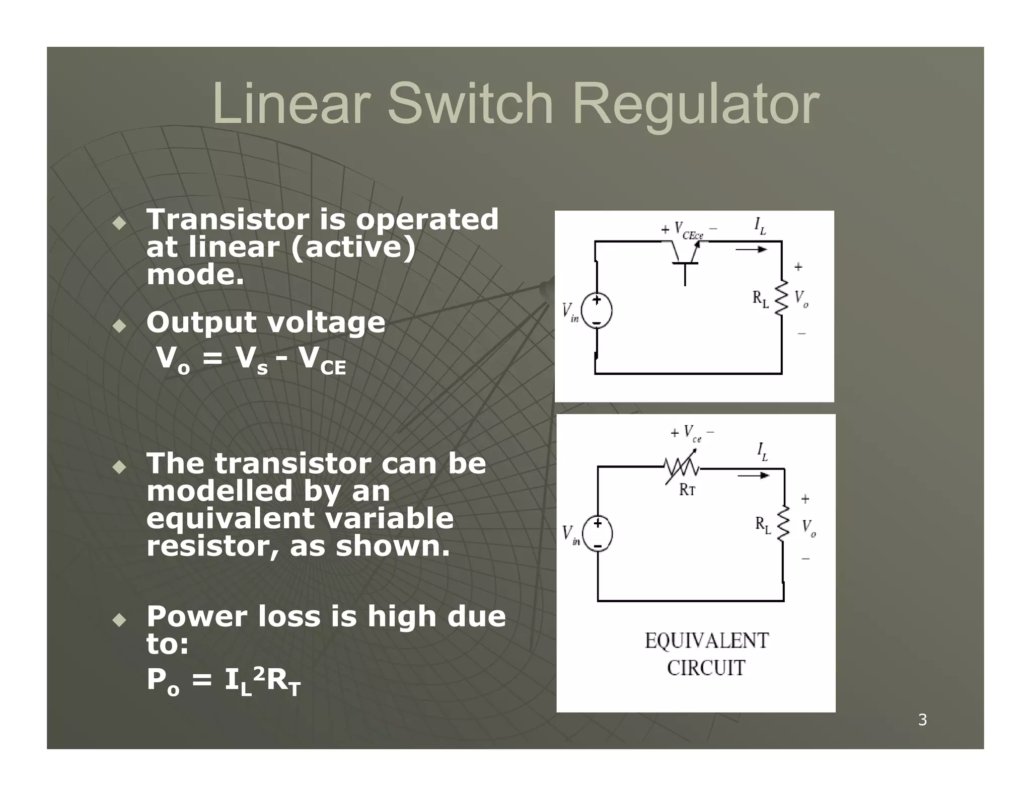
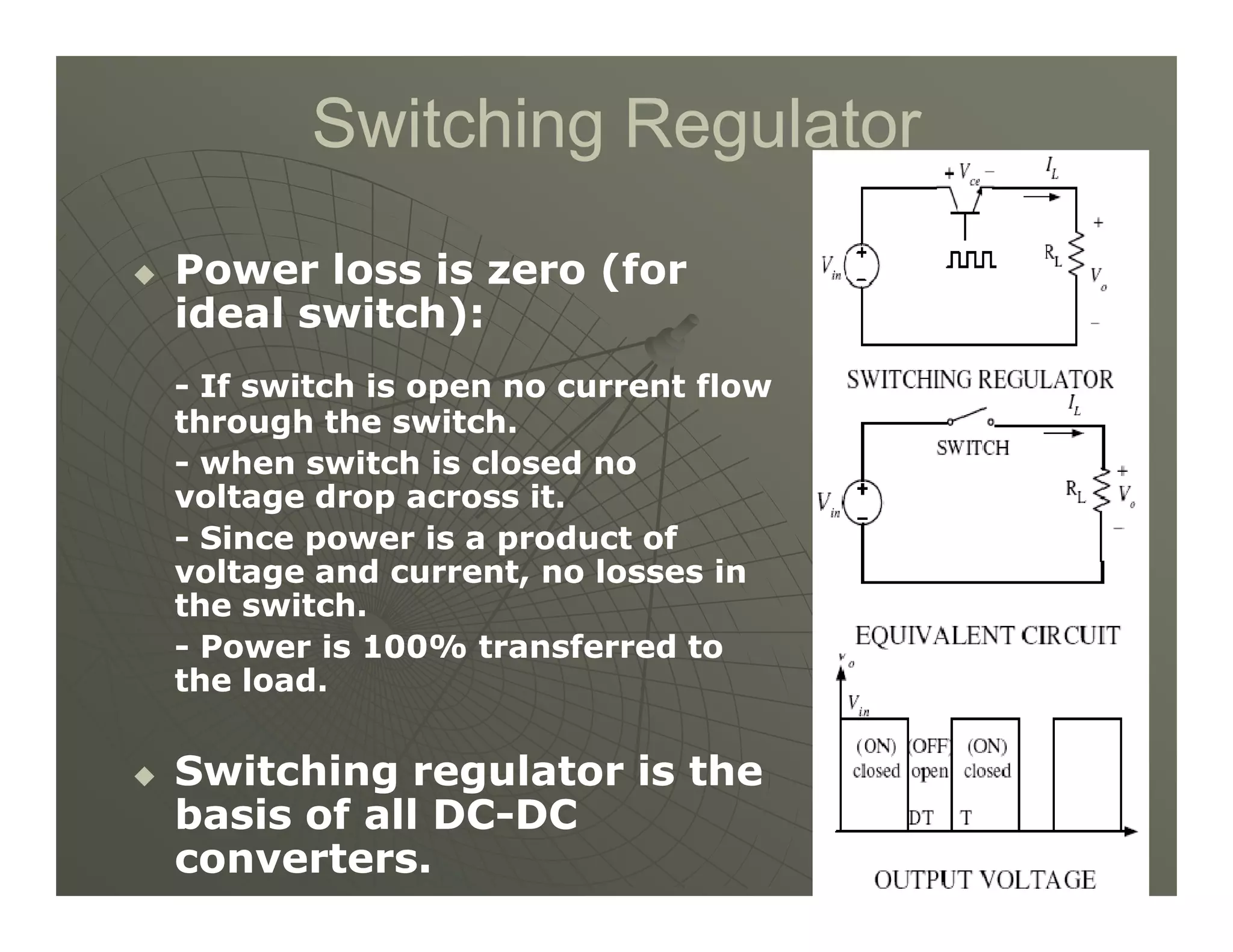
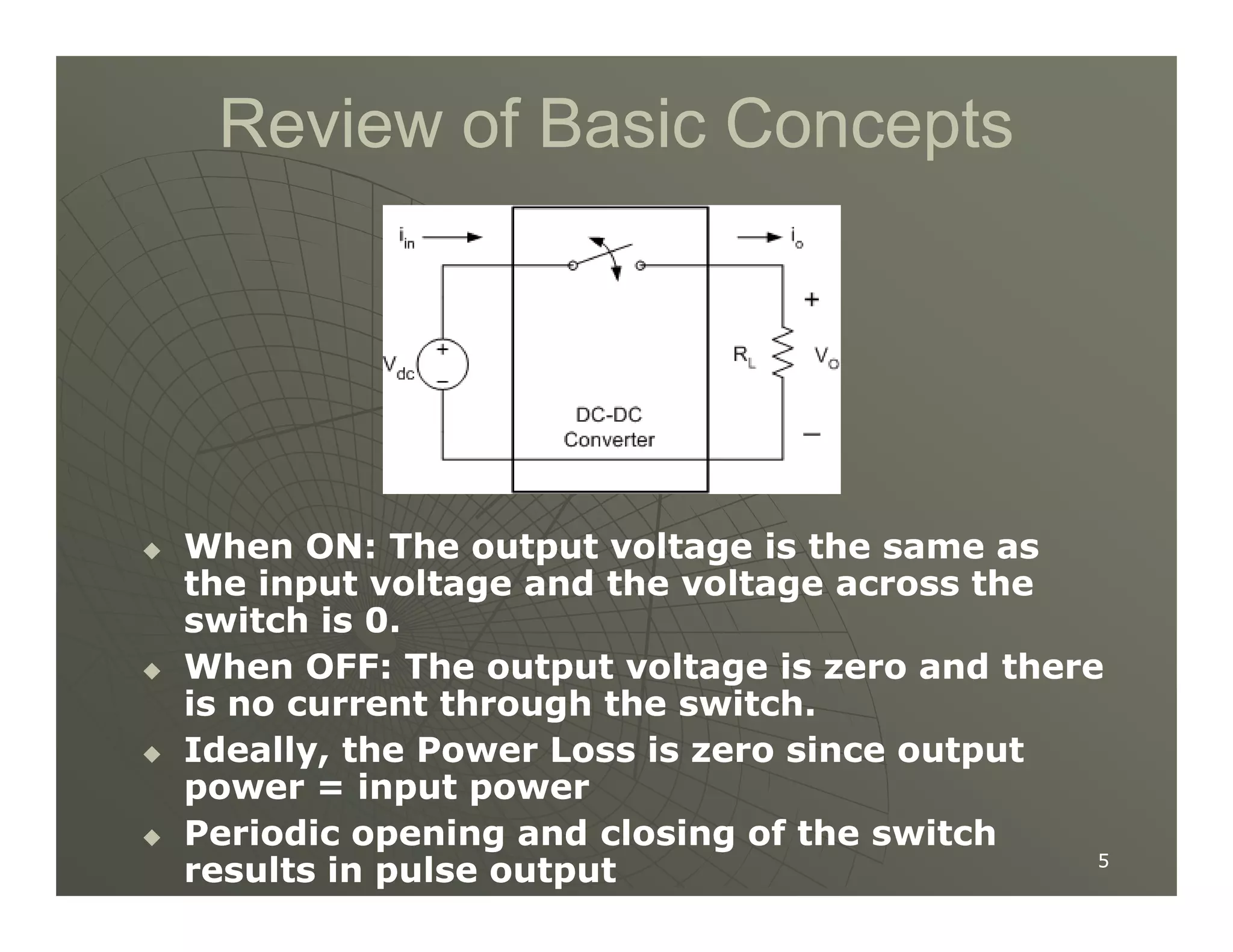
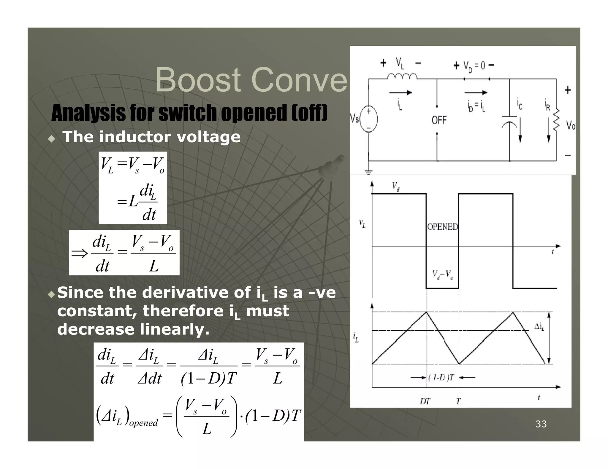
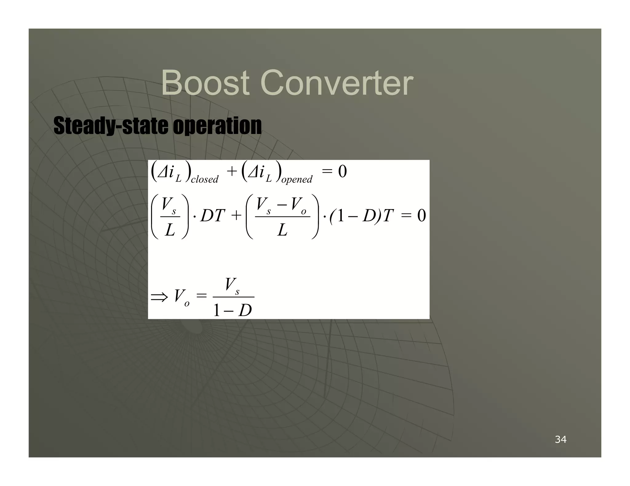
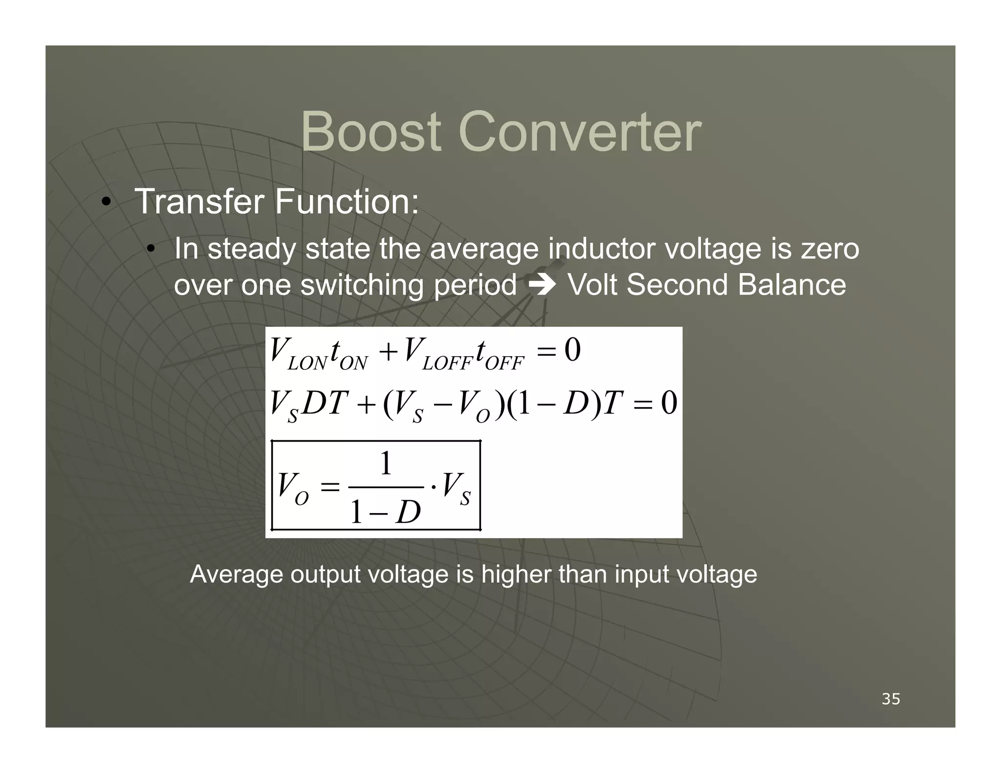
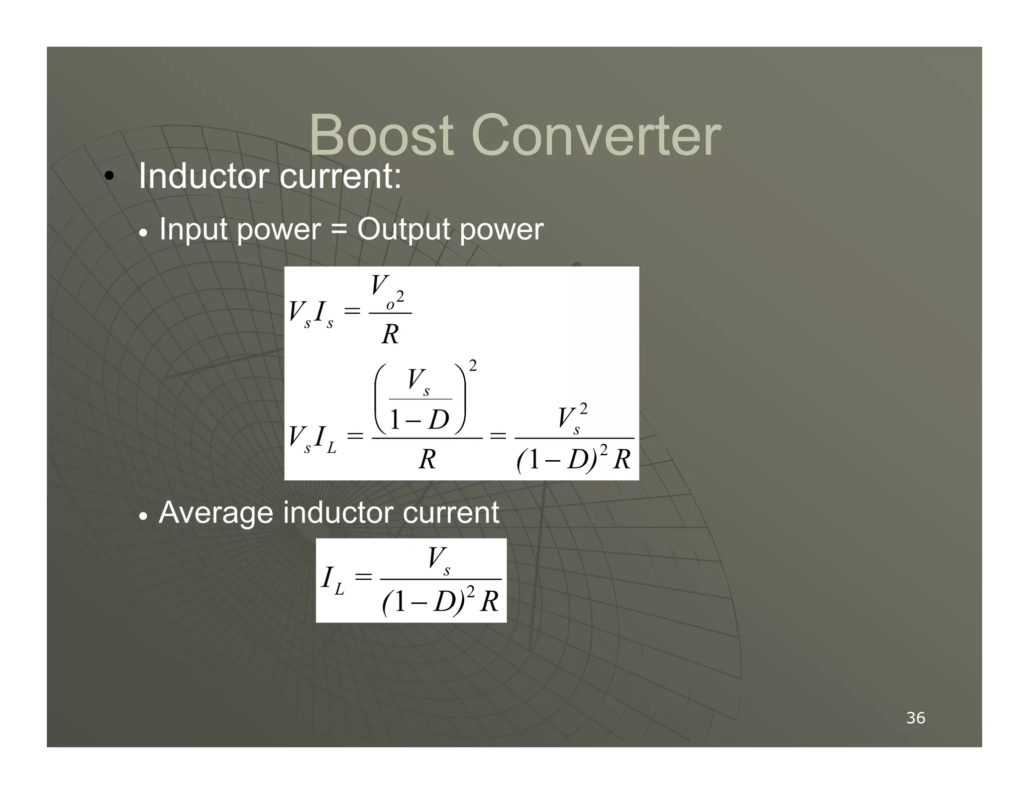
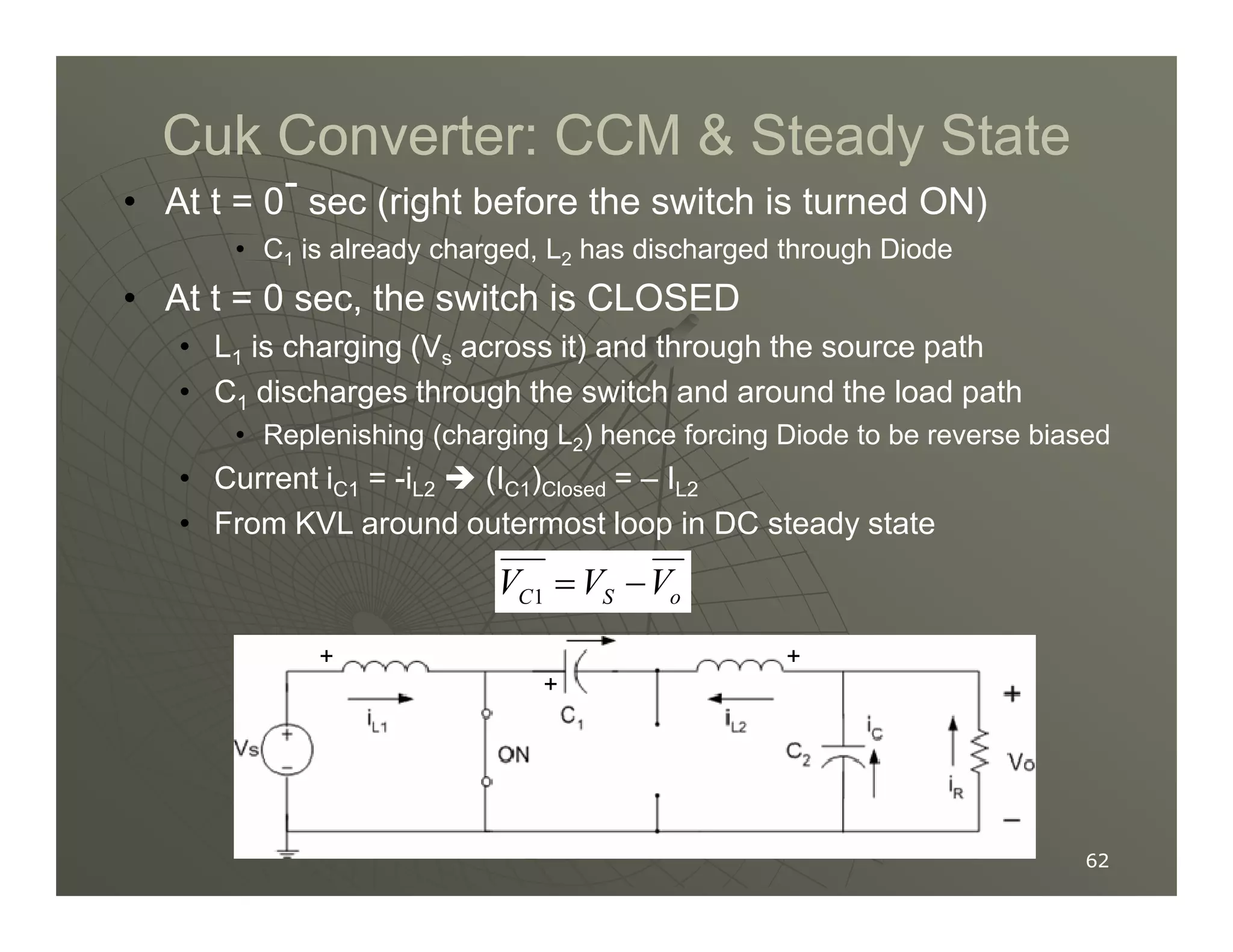
1) DC-DC converters control the output voltage by converting the unregulated DC input voltage to a regulated DC output voltage. Switching regulators have near zero power loss by rapidly opening and closing a switch to transfer power from input to output in pulses.
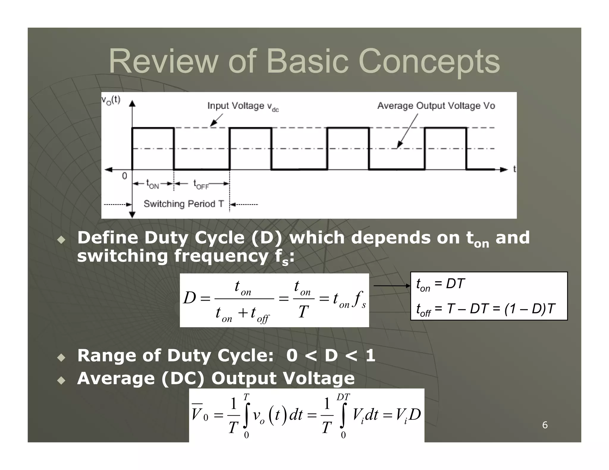
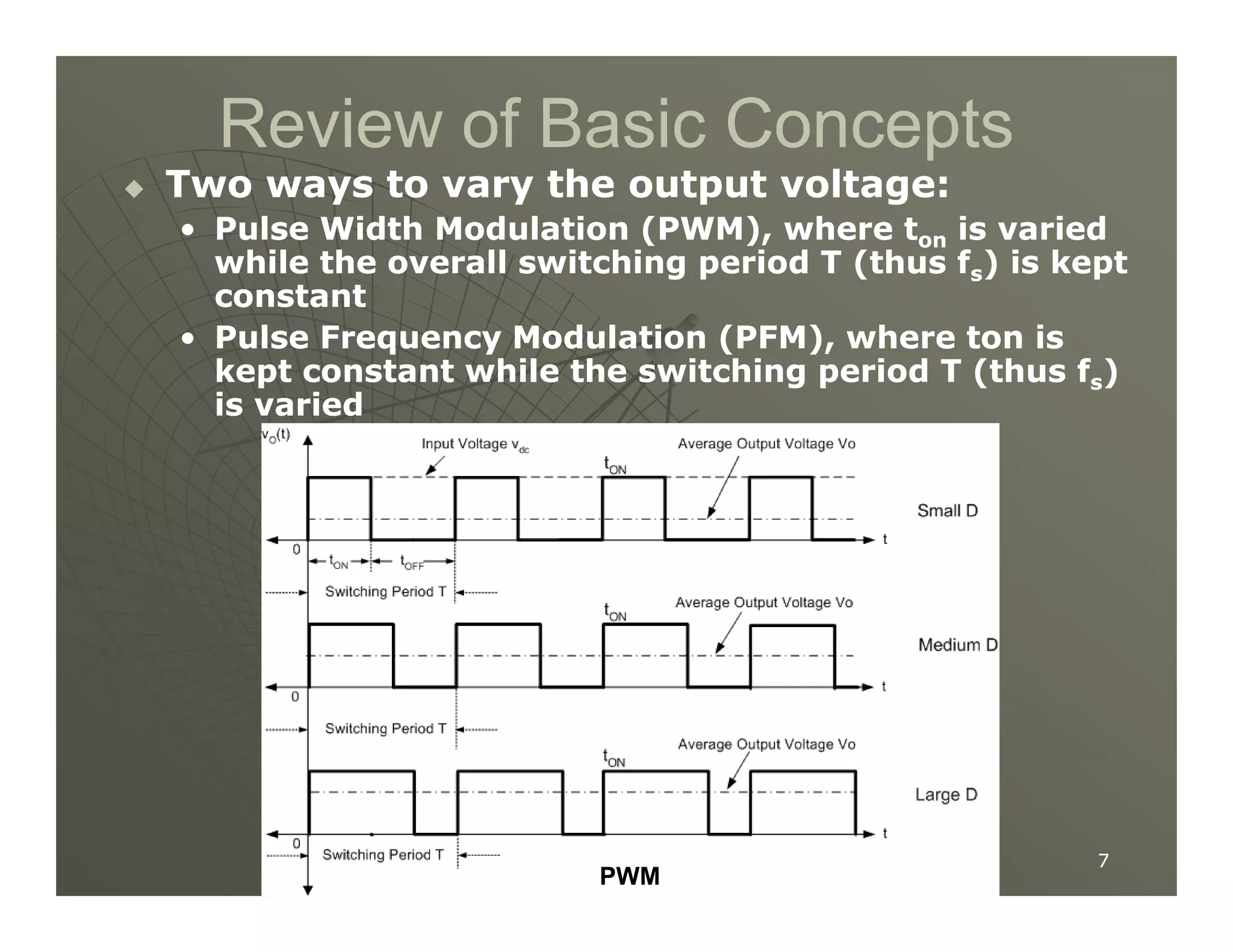
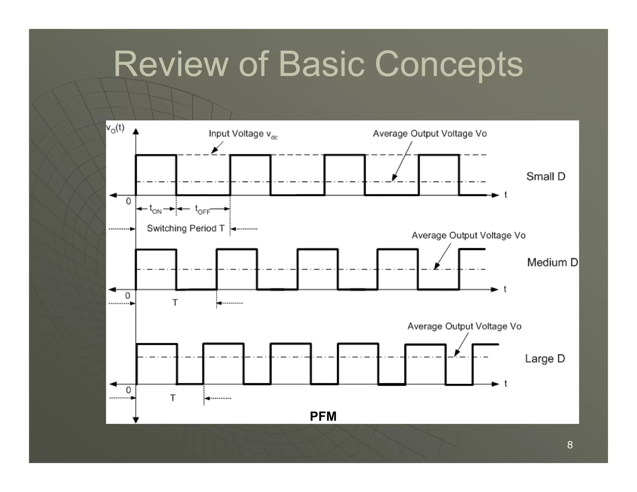
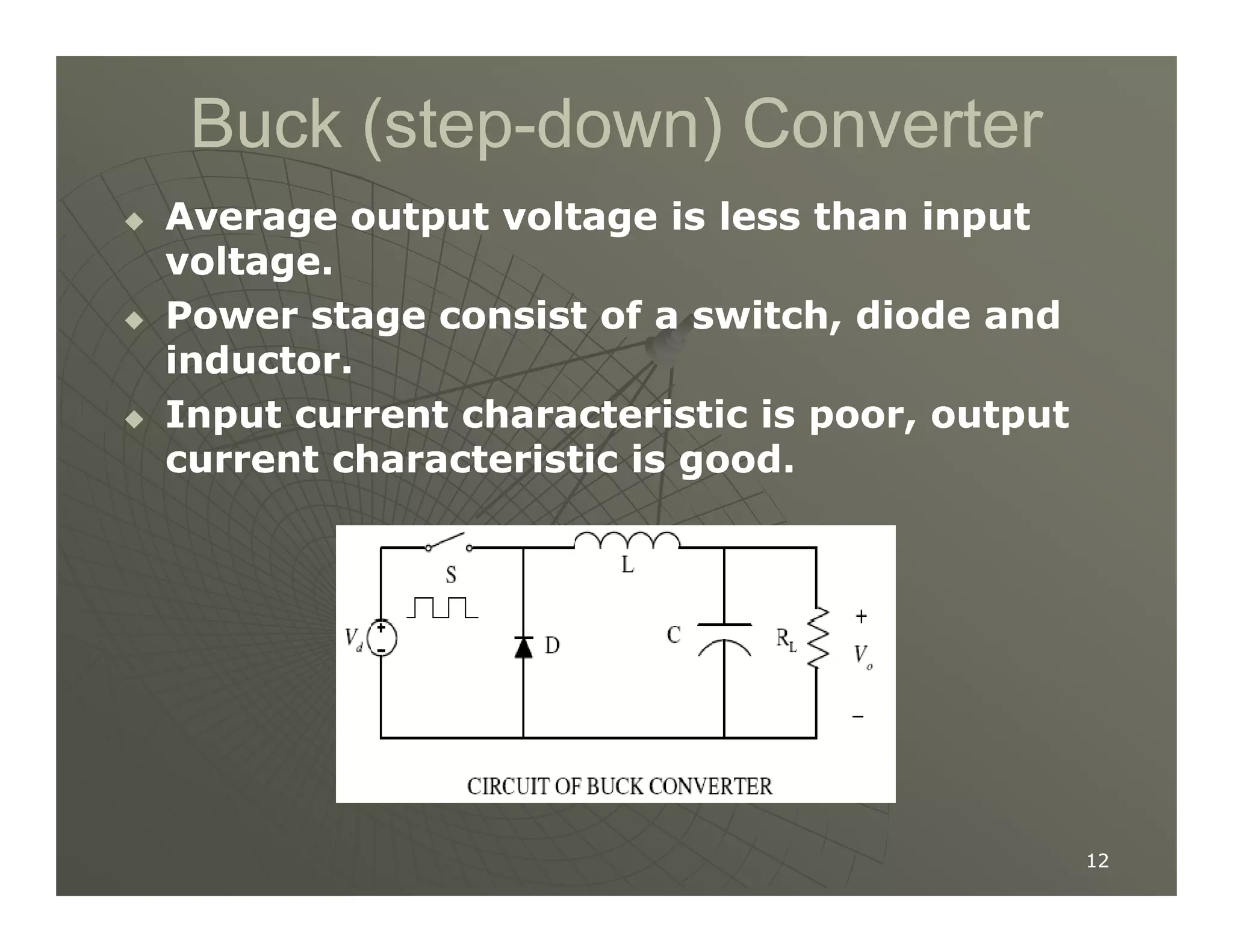
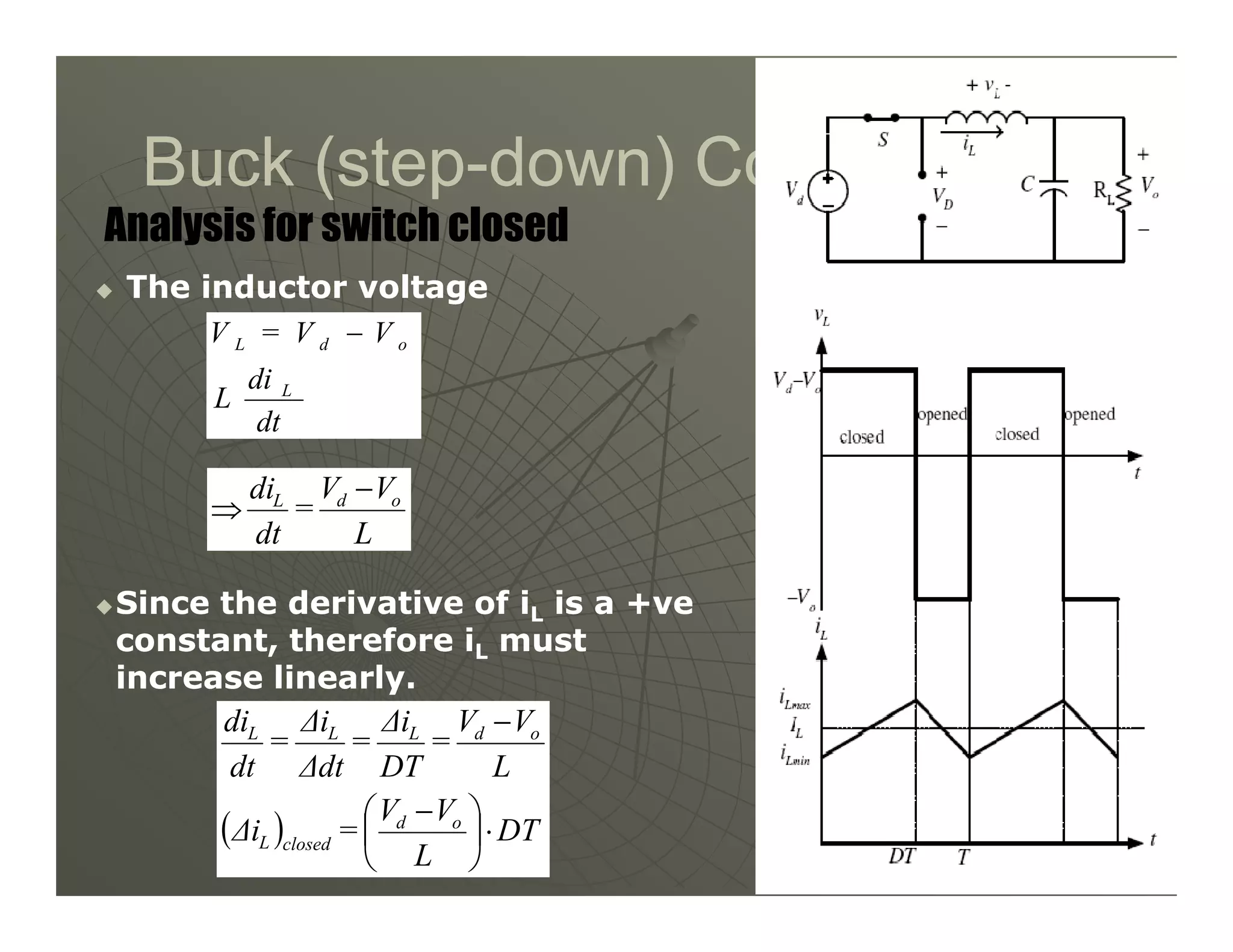
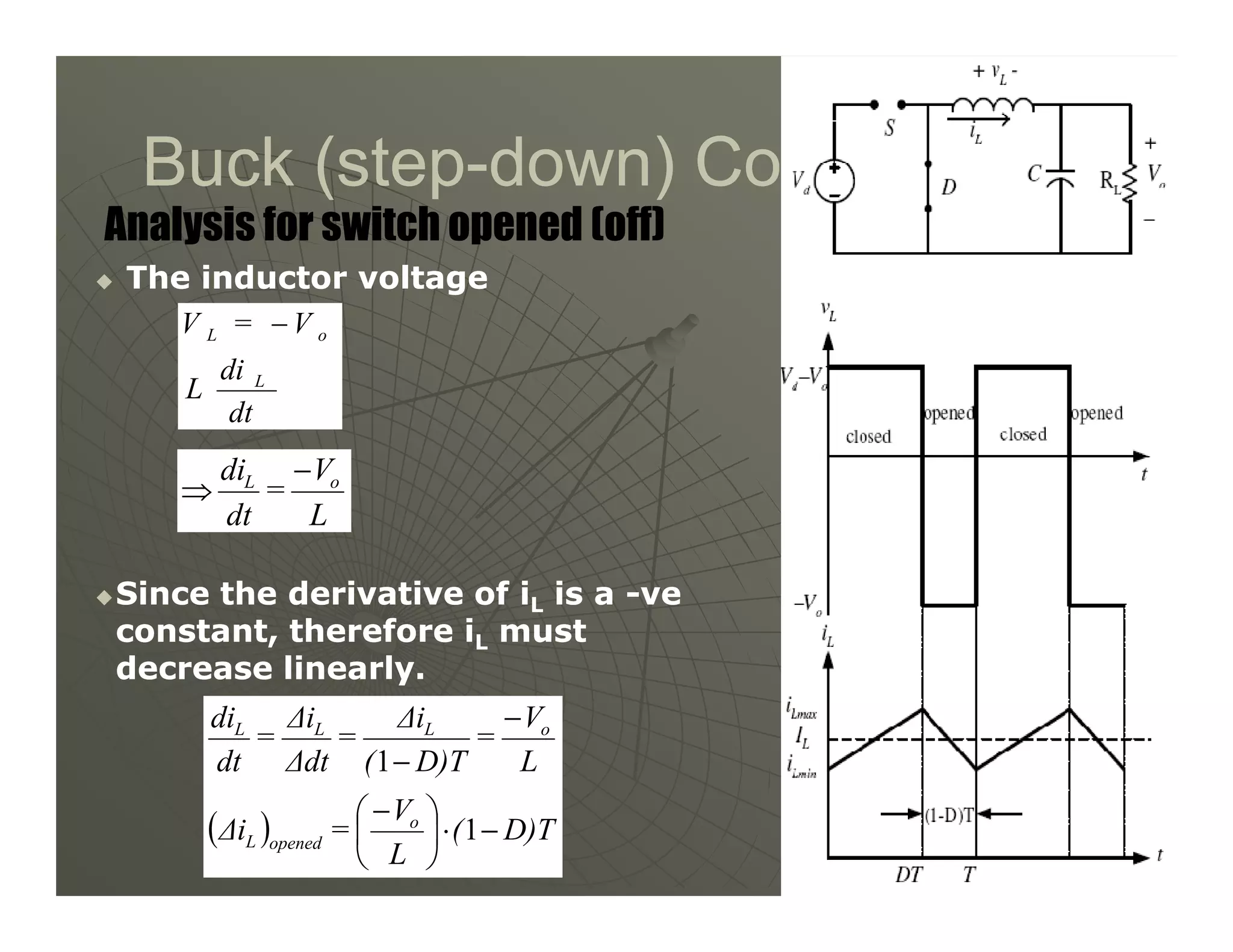
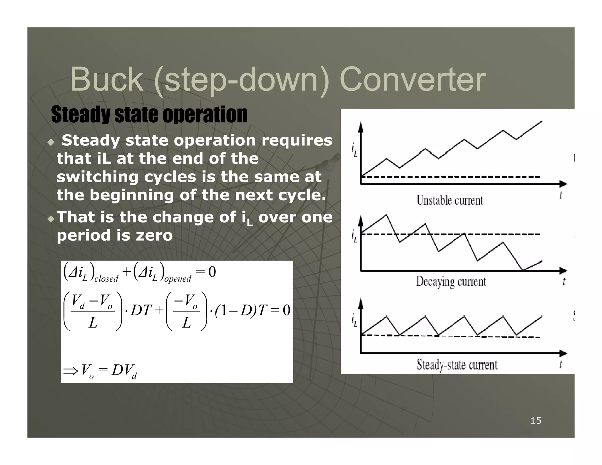
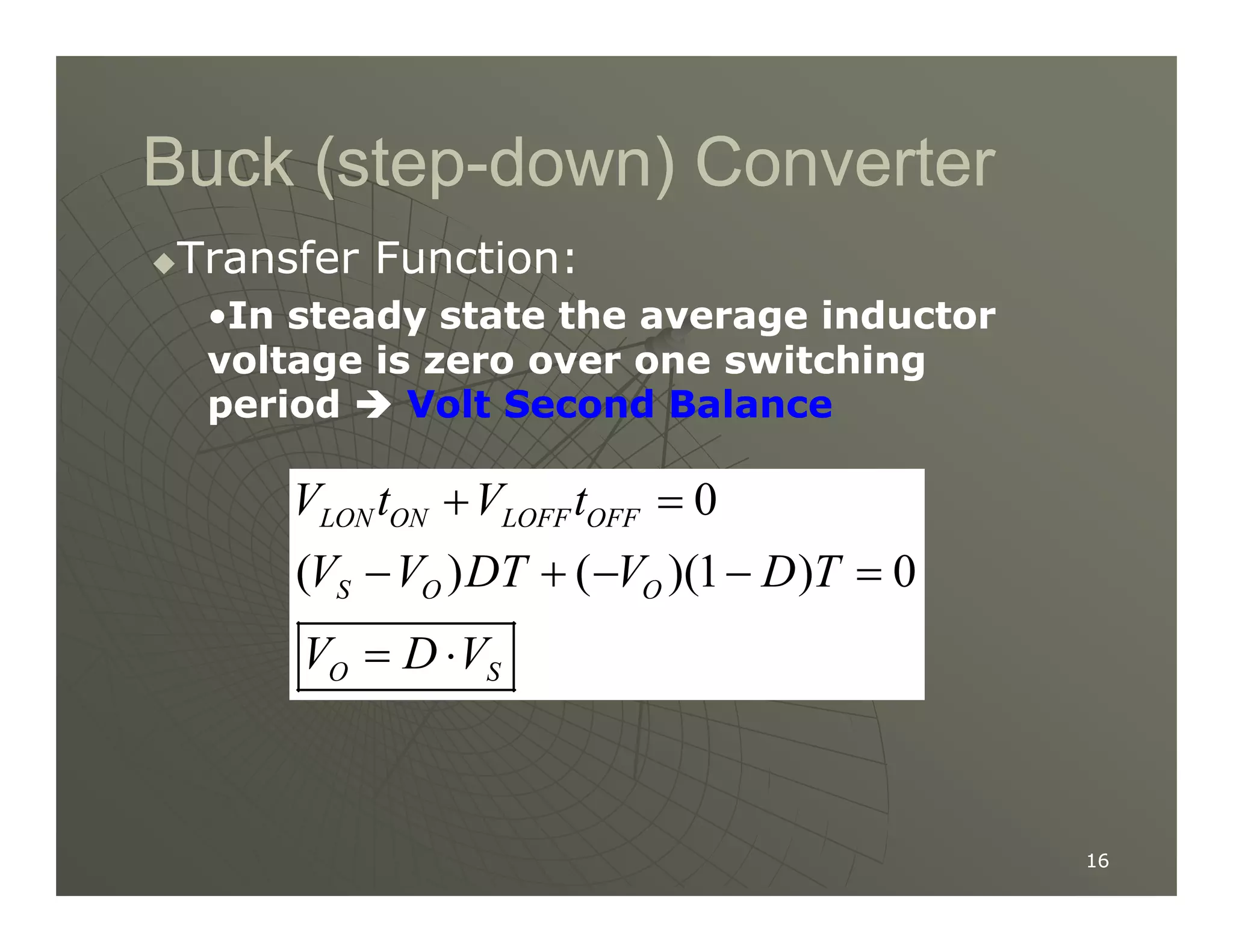
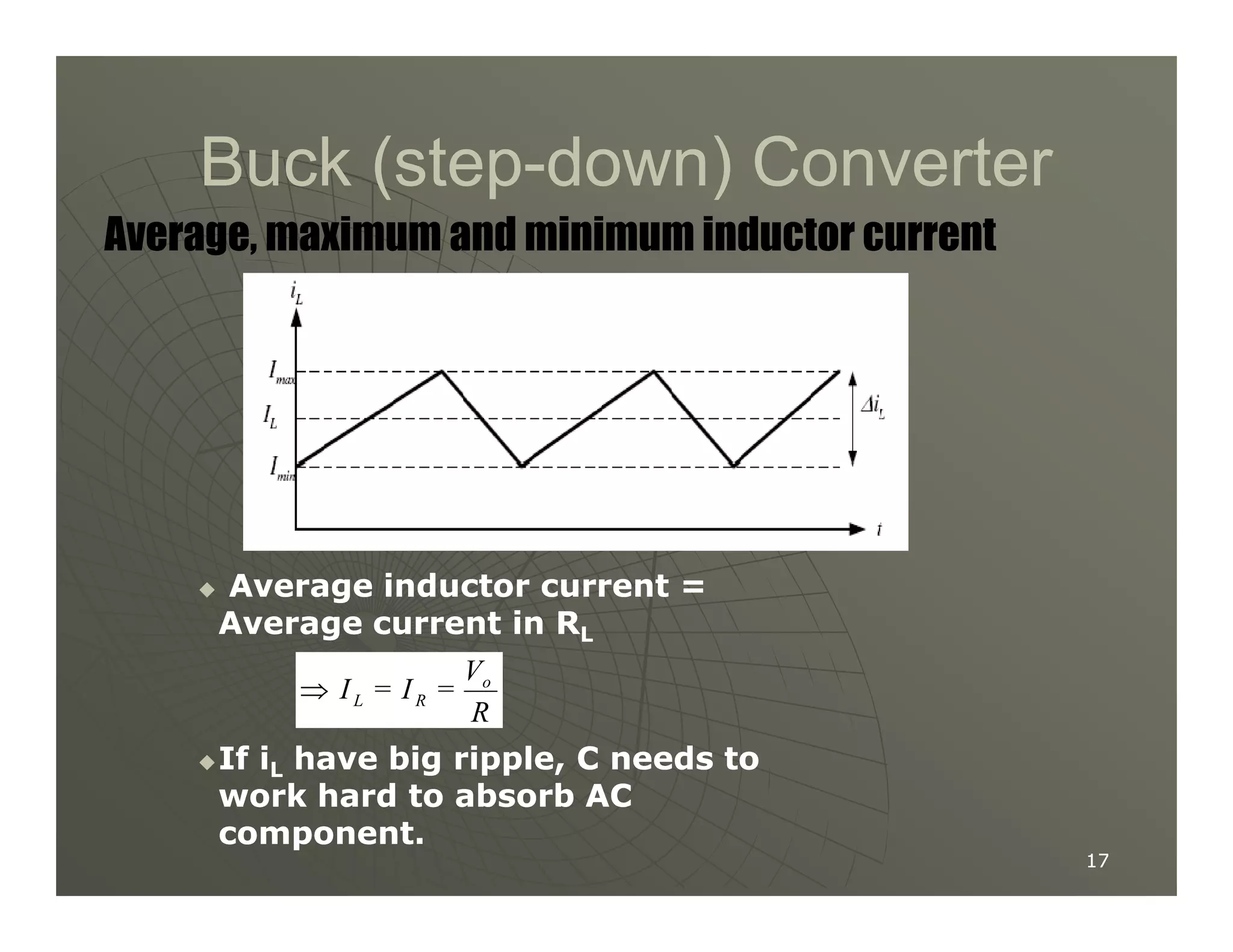
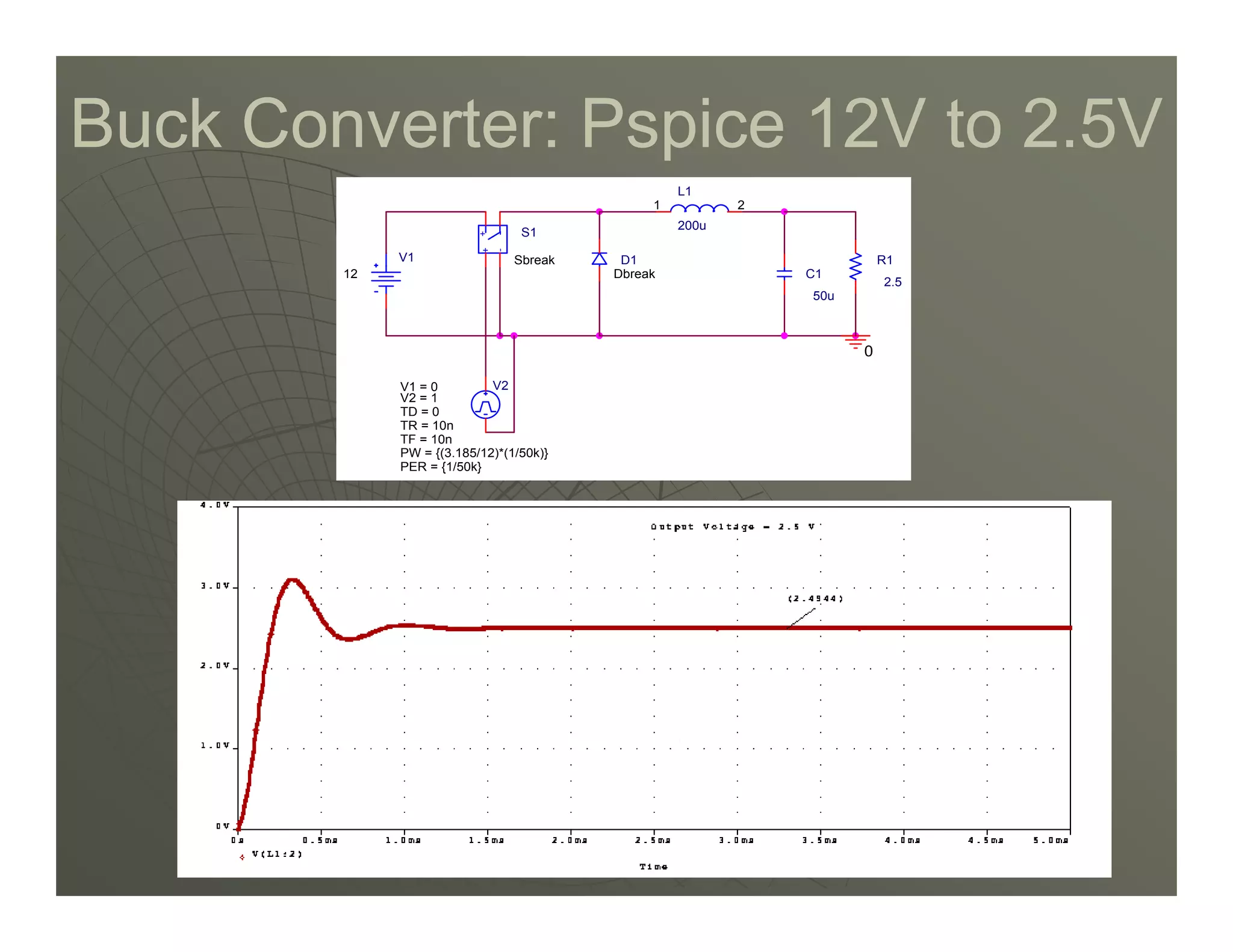
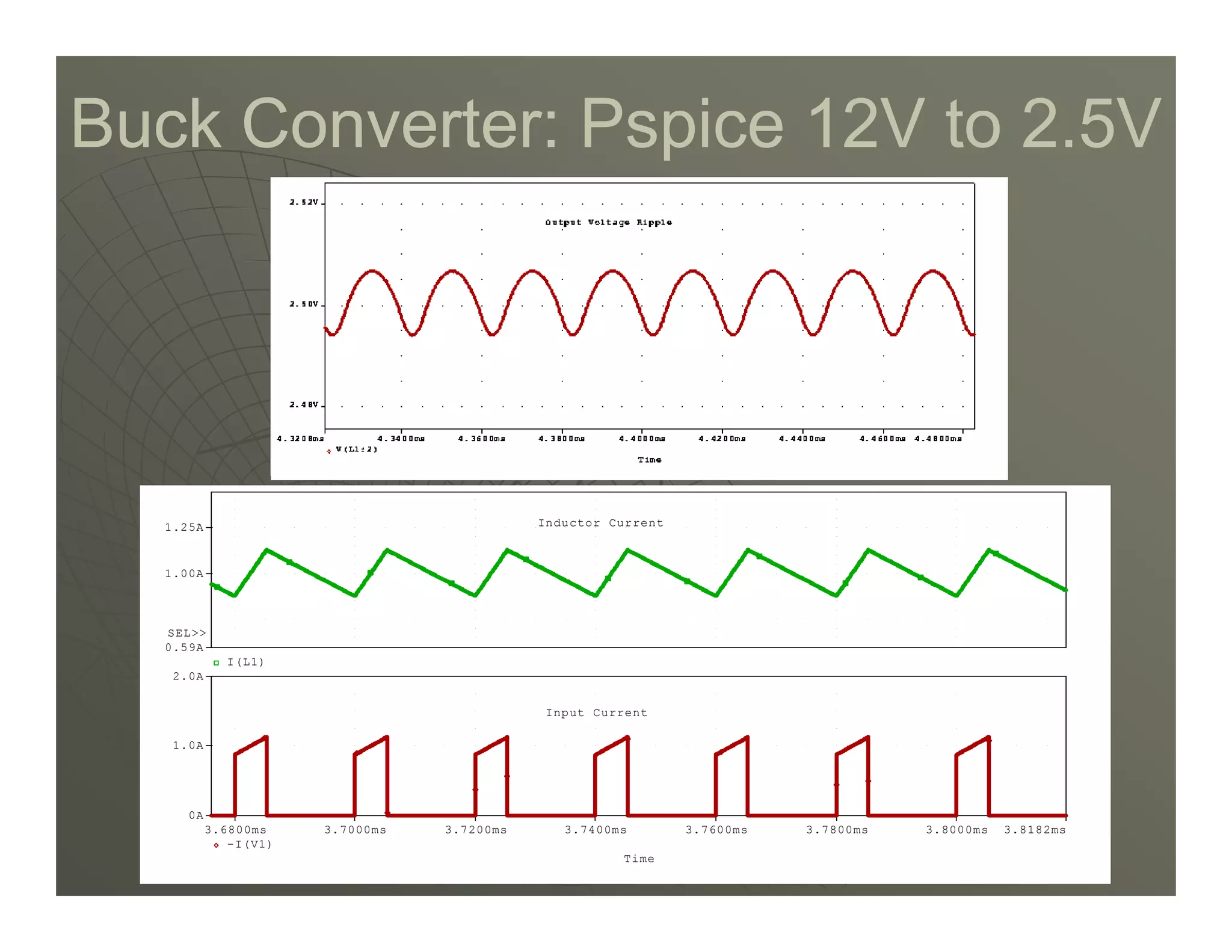
2) A buck converter is a type of step-down DC-DC converter that produces an output voltage lower than the input voltage. It contains a switch, diode, and inductor. The inductor current ripples between a maximum and minimum value depending on the duty cycle of the switch.
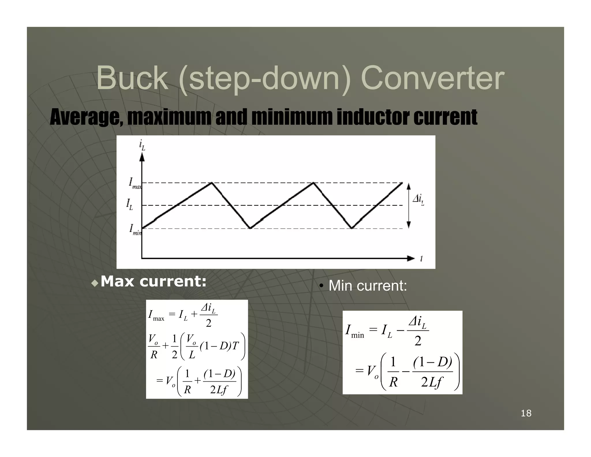
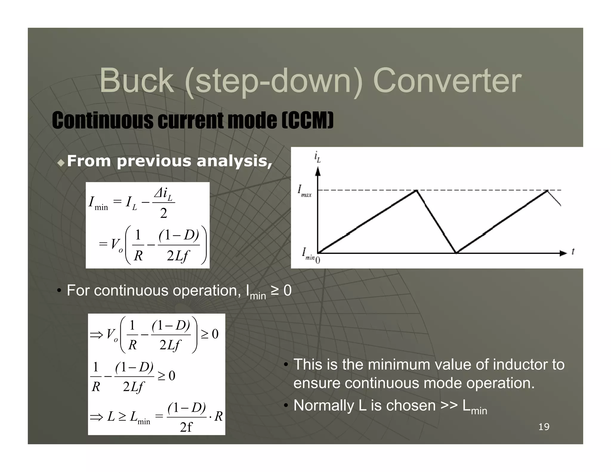
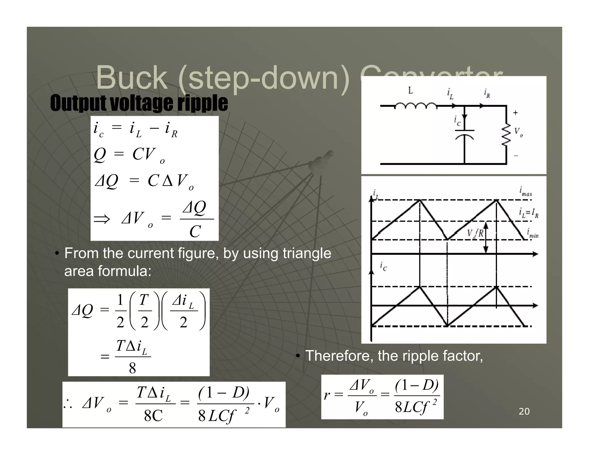
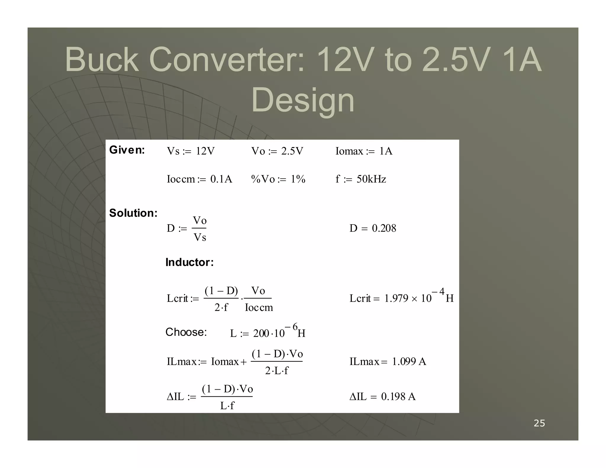
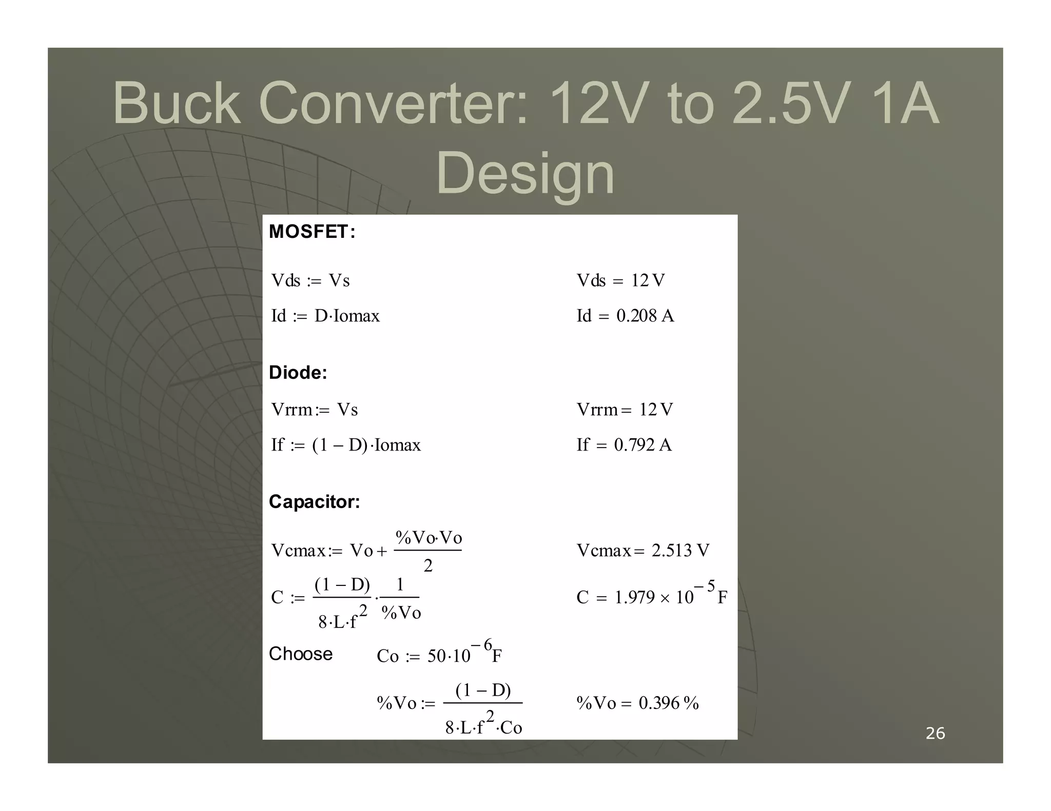
3) Key parameters in buck converter design include duty cycle, switching frequency, inductor value, and capacitor value. These are selected to achieve the desired output voltage