Pay after result spell caster (,$+27834335081)@ bring back lost lover same da...
port_tutorial_cpw (1).ppt
1. HFSS v8 Training
1
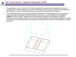
Port Tutorial Series: Coplanar Waveguide (CPW)
This presentation is one in a series of Port Tutorials, intended to help users better understand the nuances of
model excitation. With incorrect inputs, the entire 3D field solution will be incorrect. Therefore, proper attention to
port definitions can make the difference between a successful and unsuccessful HFSS analysis.
In this tutorial presentation, the user will be presented with guidelines for setting up ports on both grounded and
ungrounded coplanar waveguide (CPW) transmission line structures. Recommendations for both wave and
lumped ports will be outlined. General advice will be provided for initial port sizing, followed by diagnostic
procedures to use to evaluate whether or not a user’s ports are appropriate for their specific configuration. Pictorial
examples will be provided of grounded, ungrounded, and limited-side-ground CPW port mechanizations throughout
the tutorial.
2. HFSS v8 Training
2
Structure
Coplanar Waveguide is a transmission line system consisting of a central current-carrying trace atop a substrate,
coplanar with side grounds extending beyond a symmetric gap to either side of the trace. There are different kinds
of CPW transmission lines used in RF and microwave applications
Grounded CPW (GCPW) will have an additional ground plane on the underside of the substrate. In practice
this plane needs to be sufficiently distant from the trace as compared with the side grounds that the system
carries a CPW mode rather than a lossy microstrip mode
Ungrounded CPW is more standard, in which the side grounds coplanar to the strip itself provide the only
return current path, and the underside of the substrate is unclad.
Finite Ground CPW (FG-CPW) traditionally refers to an ungrounded CPW in which the side ground
metalization is of limited width, often not more than 2 – 3 times the width of the center trace itself, due to space
considerations.
Advantages
CPW has the same advantage as microstrip, in that the signal is carried on an exposed surface trace, on which
surface-mount components can be attached. Being a surface signal carrier it also lends itself well to testing via
ground-signal-ground type probes
Unlike microstrip, CPW (at least in the ungrounded form) has little parasitic losses between surface mounted
components and an underlying ground plane
Disadvantages
The primary disadvantage of CPW is that it is harder to design with: features such as open and shorted stubs are not
as simple as they are with microstrip or stripline. Additionally, CPW is not well supported even by many modern
transmission line calculators and circuit simulators
While obtaining the necessary dimensions for a CPW of a desired characteristic impedance is possible, often the
dimensions output by transmission line calculators are impracticable given etching constraints
If the ‘aspect ratio’ of a CPW (the ratio of its gap to trace widths) becomes too high or too low, the desired CPW
mode can be supplanted by parasitic microstrip modes or parallel slotline modes, resulting in poor performance
Coplanar Waveguide: Basic Review
3. HFSS v8 Training
3
Coplanar Waveguide: Dimensioning
CPW Dimensions
CPW is generally defined by center strip width w, gap width g, substrate height h, and substrate dielectric material
Metal thickness is also important, especially when metal thickness t 0.1w or t 0.1g
For FG-CPW, the width of the side grounds, S, must also be considered in port design
w
g
h t
4. HFSS v8 Training
4
HFSS Ports: General Requirements
Purpose
A Port is a 2D surface on which the fields will be solved according to Maxwell’s Equations to determine appropriate
RF modal excitations into the 3D model volume. Think of a port as an “aperture” in which the field distribution and
orientation is known for the steady-state finite element solution
Wave ports solve actual field distributions in transmission line cross-sections. Lumped ports excite simplified field
distributions to permit S-parameter outputs where wave ports are not feasible.
Characteristics
Port surface area takes on the material characteristics of the materials which touch its face
Wave Port boundaries take on the boundary characteristics of the boundaries which share its edges
Edges touching perfect_e faces, such as ground planes, become perfect_e edges for the port computation
Edges touching perfect_h faces become perfect_h edges for the port computation
Edges touching symmetry faces take on the definition of the appropriate perfect_e or perfect_h type
Edges touching radiation faces, however, default to perfect_e conductive boundary conditions!
The environment variable ZERO_ORDER_ABC_ON_PORT = 1 can set them to 377 ohms instead
Due to the port bounding edges, which may not match boundaries on field behavior in the full 3D volume around the
transmission line past the port plane, proper port sizing and location is crucial
A microstrip port at left has
sufficient surface area for fringing
field behavior, while the one at
right forces field attachment to the
port side walls, even if the
surrounding area was designated
as a radiation boundary
5. HFSS v8 Training
5
CPW Wave Ports: Starting Recommendations
Wave Port Size
The standard recommendation for most CPW wave ports is a rectangular aperture
Port width should be no less than 3 x the overall CPW width, or 3 x (2g + w)
Port height should be no less than 4 x the dielectric height, or 4h
If no convenient ‘solid face(s)’ meet the above sizing requirements, draw a 2D rectangle for the Port.
Wave Port Location
The wave port should be centered horizontally on the CPW trace
If the port is on GCPW, the port bottom edge should lie on the substrate bottom ground plane
If the port is on ungrounded CPW, the port height should be roughly centered on the CPW metal layer
Wave Port Restrictions
As with all wave ports, there must be only one surface normal exposed to the field volume
Port should be on exterior model face, or capped by a perfect conductor block if internal
The wave port outline must contact the side grounds (all CPWs) and bottom ground (GCPW)
The wave port size should not exceed lambda/2 in any dimension, to avoid permitting a rectangular waveguide
modal excitation
3 (2g + w)
w
h
4h minimum
g
Ungrounded CPW Grounded CPW
3 (2g + w)
w
h
4h minimum
g
6. HFSS v8 Training
6
CPW Wave Ports: Impedance and Calibration
Impedance Lines
Optional for wave ports, but if Zpv and Zvi desired, should be drawn
Extend from either side ground to proximal point on trace, colinear with top edge of substrate
Port width should be no less than 3 x the overall CPW width, or 3 x (2g + w)
Port height should be no less than 4 x the dielectric height, or 4h
Calibration Lines
Optional for wave ports, used only if phase referencing between multiple ports (for transmission phase parameters)
are important
The calibration line can be identical to the Impedance line.
GCPW
For grounded CPW, the Impedance and Calibration lines usually still extend from side ground to trace. However at
the user’s discretion it may be desired to run the lines from the underlying ground to the trace instead.
Usually this line orientation would only be desirable if the dielectric thickness is on the same order as the gap width
of the CPW geometry. Use the port field distribution as an indication of which ground location is more important to
your particular mode shape
7. HFSS v8 Training
7
CPW Wave Ports: Desired Excitation
Modal Field Distribution
CPW E Field distributions are shown in the images below
Basic vector fields can be displayed in Setup Executive Parameter/Port Impedances, by highlighting a port and
using the Port Fields button beneath the graphical window to adjust the vectors
CPW fields should be symmetric to either side of the center trace, with E fields extending from each ground to
the trace (or vice versa) in phase. H fields circulate around the center trace
In GCPW, field lines may also extend from the bottom ground to the center trace
Fields should not extend strongly to the port periphery, except for the bottom ground if appropriate
Characteristic Impedance
CPW modes are quasi-TEM, so the three available definitions of characteristic impedance Zpi, Zpv, and Zvi should
be nearly the same
CPW characteristic impedance should remain relatively flat with respect to frequency
Ungrounded CPW mode …and Grounded CPW mode
h
h
8. HFSS v8 Training
8
CPW Wave Ports: Diagnosing Problems from Fields, part 1
Problem 1: Port Fields don’t match CPW distribution, but extend through port window
May extend through substrate, or through air above metal surfaces [bottom, left]
Caused by too wide a port, resulting in TE01 waveguide type mode distribution (the small ‘gaps’ in the metal outline
aren’t enough to prevent this mode from existing, if given enough area)
Solution: Reduce width of port until it is below lambda/2. For GCPW, may need width below lambda/2 in substrate
Problem 2: Port Fields extend from trace to side or top edges of port window
Caused by too narrow or squat a port [bottom, right]
Solution: Increase port width or height, appropriately, to reduce field attachment
Problem 3: Port Fields are Asymmetric (very rare)
One gap appears excited, while the other is ignored: single “slotline” excitation
Usually related to high aspect ratio CPW, narrow conductor gaps, low frequencies with respect to physical size,
and/or finite metals solved “inside”
Solution: Try using ‘virtual objects’ to assist port meshing in both gaps. Or, if entire 3D model is symmetrical, solve
½ of problem space using a perfect_h symmetry condition
(Note: This problem should not frequently occur in HFSS 8.0.25 or newer)
9. HFSS v8 Training
9
CPW Wave Ports: Diagnosing Problems from Fields, part 2
Why must port outline touch side grounds?
If port outline does not contact side grounds, the port ‘window’ sees three possible signal traces inside the ‘ground
reference’ of the port perimeter [below, left]
Mode solved will be ‘even’ or first mode of three possible TEM modes in this system, not that of CPW excitation
What if I have an FG-CPW and I can’t make the port window touch the grounds without
making it too narrow?
Consider making a port window with inward-pointing ‘fingers’ that contact the side grounds [black outline, below right]
Although this appears to be creating a ‘mismatch’ to the 3D geometry (by artificially extending the side grounds at
the port plane only) remember it is only necessary to remove the vertical perfect_e port edges from proximity to the
CPW trace, permitting field lines to connect from the trace to the side grounds without perturbation. Therefore the
mode generated should not be mismatched to the 3D geometry interior to the port face (inset, bottom right).
10. HFSS v8 Training
10
CPW Wave Ports: Diagnosing Problems from Impedance
Problem 1: Impedance too low, but stable with respect to frequency
Suspect port outline not contacting side grounds, permitting three floating conductors in “even” mode (see last page)
Solution: Assure port outline contacts side grounds
Suspect port too narrow or too short vertically, permitting port edges to act as grounds that should not exist. Or
perhaps port bottom was placed colinear with bottom of substrate, when grounded CPW was not intended
Solution: Correct port size and/or placement to move unwanted grounding edges further from CPW trace.
Problem 2: Zpi, Zpv, Zvi give very different results, with strong frequency dependence
Suspect solution of a rectangular waveguide-like mode in substrate or air, due to a too-large port
Solution: Reduce port width to below lambda/2 in appropriate material.
Zo > Zo for CPW mode
Waveguide-like frequency
dependence in Zo
11. HFSS v8 Training
11
CPW Lumped Ports: Layout and Sizing
Lumped Ports can be used for Internal CPW excitations
Also referred to as Gap Source Ports since they excite uniform ‘gap-like’ E fields, yet still permit S-parameter output
Lumped port boundaries are conductive where touching conductors, or perfect_h boundaries where not
Will not provide impedance or propagation results; instead S-parameters referenced to user-provided impedance
Simulate the measurements gathered by Ground-Signal-Ground probes very well (e.g. in on-Silicon component
analysis)
Useful for CPW on very thick substrates relative to trace and gap widths (e.g. on-Silicon again)
Sizing
Connect side grounds together just beyond the ‘end’ of the center trace
Assign port to a rectangle which connects the center trace to the joined ground, in line with the center trace
Width of port should be no larger than the CPW trace itself
Length of port should be roughly equal to width (too long ignores inductive component, too squat ignores
capacitive-like component)
Port should lie coplanar to top of substrate, even if 3D metal objects are in use
Required impedance and calibration lines should extend from ground to trace consistently for all ports
Zo > Zo for CPW mode
G S G
Port