Download to read offline

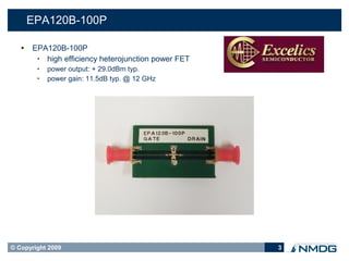
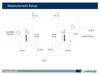
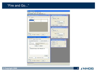
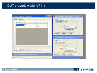
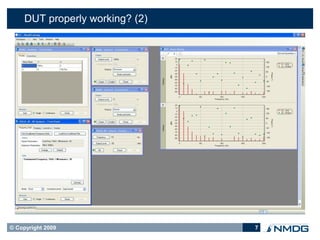
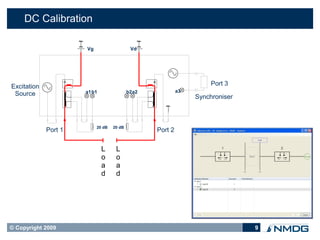
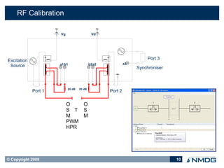
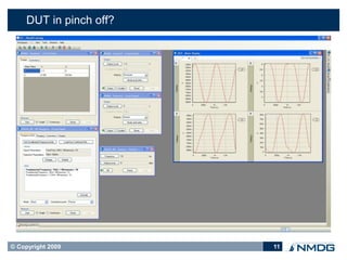
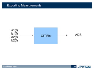
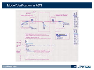
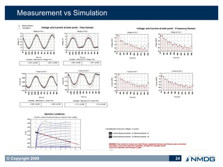

The document describes characterization and reliability testing of the EPA120B-100P transistor using the ZVxPlus application. It outlines the measurement setup and calibration process, and demonstrates DC and RF transistor characterization through IV curves, S-parameters, and time domain signals. Advanced displays show dynamic load lines and small-signal parameters. Measurements are exported to ADS for model verification.