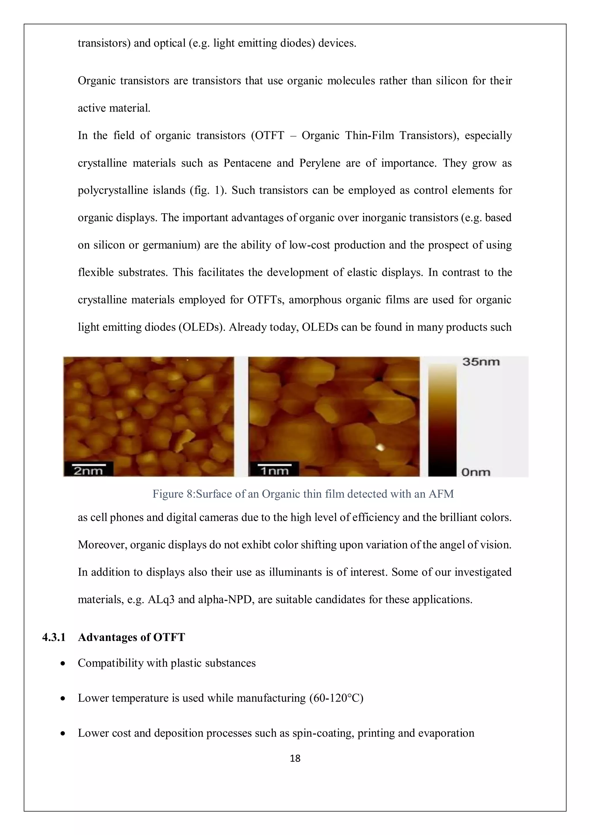
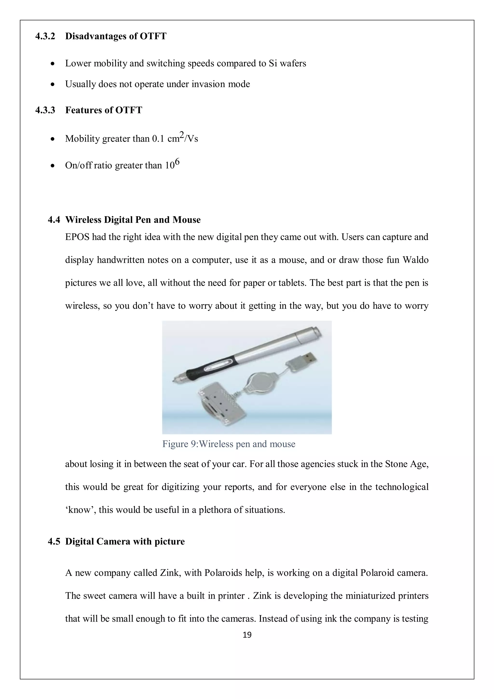
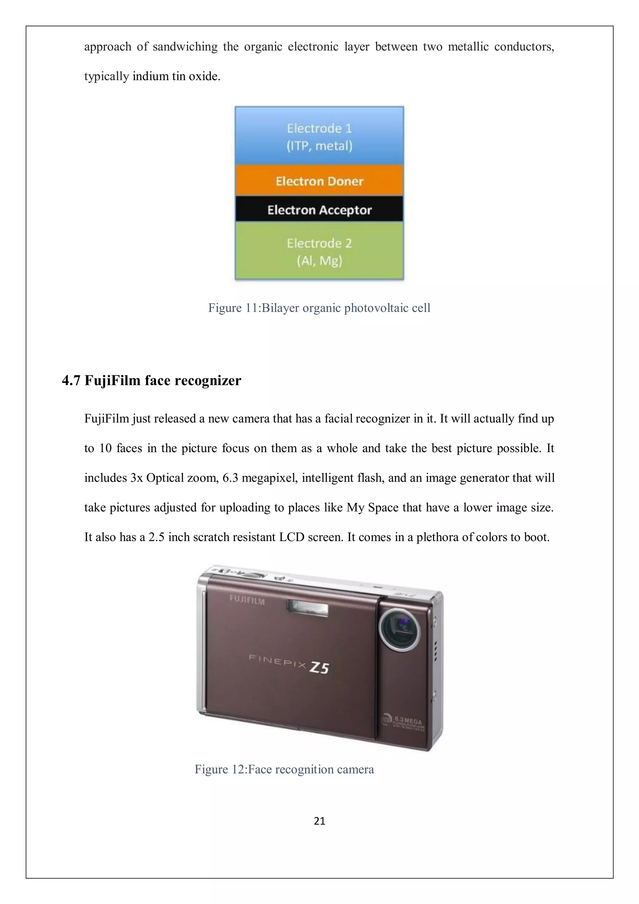
Conducting polymers have extended p-orbital system, through which electrons can be moved from one end to another and of polymer. Also, when a polymer is doped, there are changes in it due to resonance the charge can drift through the chain, and generating the conductivity.
TRANSPARENT ELECTRONICS
Abstract: Transparent electronics is an emerging science and technology field focused on producing ‘invisible’ electronic circuitry and opto-electronic devices.
Applications include consumer electronics, new energy sources, and transportation; for example, automobilewindshields could transmit visual information to the driver. Glass in almost any setting could also double as an electronic device, possibly improving security systems or offering transparent displays. In a similar vein, windows could be used to produce electrical power. Other civilian and military applications in this research field include realtime wearable displays.
As for conventional Si/III–V-based electronics, the basic device structure is based on semiconductor junctions and transistors. However, the device building block materials, the semiconductor, the electric contacts, and the ielectric/passivation layers, must now be transparent in the visible –a true challenge! Therefore, the first scientific goal of this technology must be to discover,understand, and implement transparent high-performance electronic materials. The second goal is their implementation and evaluation in transistor and circuit structures.
The electronics during the past 10 years, the classes of materials available for transparent electronics applications have grown dramatically. Historically, this area was dominated by transparent conducting oxides (oxide materials that are both electrically conductive and optically transparent) because of their wide use in antistatic coatings, touch display panels, solar cells, flat panel displays, heaters, defrosters, ‘smart windows’ and optical coatings. All these applications use transparent conductive oxides as passive electrical or optical coatings. The field of transparent conducting oxide (TCO) materials has been reviewed and many treatises on the topic are available. However, more recently there have been tremendous efforts to develop new active materials for functional transparent electronics. These new technologies will require new materials sets, in addition to the TCO component, including conducting, dielectric and semiconducting materials, as well as passive components for full device fabrication.
COMBINING OPTICAL TRANSPARENCY WITH ELECTRICAL CONDUCTIVITY
Transparent conductors are neither 100% optically transparent nor metallically conductive. From the band structure point of view, the combination of the two properties in the same material is contradictory: a transparent material is an insulator which possesses completely filled valence and empty conduction bands; whereas metallic conductivity appears when the Fermi level lies within a band with a large density of states to provide high carrier concentration. Efficient transparent conductors find their niche in a compromise between a sufficient transmission within the visible spectral range and a moderate but useful in practice electrical conductivity.
Research Inventy : International Journal of Engineering and Science is published by the group of young academic and industrial researchers with 12 Issues per year. It is an online as well as print version open access journal that provides rapid publication (monthly) of articles in all areas of the subject such as: civil, mechanical, chemical, electronic and computer engineering as well as production and information technology. The Journal welcomes the submission of manuscripts that meet the general criteria of significance and scientific excellence. Papers will be published by rapid process within 20 days after acceptance and peer review process takes only 7 days. All articles published in Research Inventy will be peer-reviewed.
Fabrication and studying the dielectric properties of (polystyrene-copper oxi...journalBEEI
The preparation of (polystyrene-copper oxide) nanocomposites have been investigated for piezoelectric application. The copper oxide nanoparticles were added to polystyrene by different concentrations are (0, 4, 8 and 12) wt.%. The structural and A.C electrical properties of (PS-CuO) nanocomposites were studied. The results showed that the dielectric constant and dielectric loss of (PS-CuO) nanocomposites decrease with increase in frequency. The A.C electrical conductivity increases with increase in frequency. The dielectric constant, dielectric loss and A.C electrical conductivity of polystyrene increase with increase in copper oxide nanoparticles concentrations. The results of piezoelectric application showed that the electrical resistance of (PS-CuO) nanocomposites decreases with increase in pressure.
Synthesis of (Poly-methyl Methacrylate-lead Oxide) Nanocomposites and Studyin...journalBEEI
Piezoelectric materials have been prepared from (poly-methyl methacrylate-lead oxide) nanocomposites for electronic applications. The lead oxide nanoparticles were added to poly-methyl methacrylate by different concentrations are (4, 8, and 12) wt%. The structural and dielectric properties of nanocomposites were studied. The results showed that the dielectric constant and dielectric loss of nanocomposites decrease with increase in frequency of applied electric field. The A.C electrical conductivity increases with increase in frequency. The dielectric constant, dielectric loss and A.C electrical conductivity of poly-methyl methacrylate increase with increase in lead oxide nanoparticles concentrations. The results of pressure sensor showed that the electrical resistance of (PMMA-PbO2) nanocomposites decreases with increase in pressure.
Transient Electronics: as per the name defines itself "lasting only for a short time"these devices can very well be used in covert operations where they can simply disappear after serving their purpose.Help in reducing e-waste.
Since many years we are facing the problem of breaking wires due to human activities or natural calamity. So why not we try to construct a wire that have far greater elasticity than our normal copper & aluminum wire without affecting it’s conductivity. Using elastic polymers we can create such wires. Any Polymer wire that is structured like a hollow cylinder of desired diameter and filled with conductive liquid, can have a effective quality to provide a conductive path for the movement of electrons and ions after connecting its ferrous ends to the voltage sources. Not only this wire can provide us a super elastic wire but also it reduce the power loss that normally occurs due to the resistance of the conducting metal of the wire. This will directly affect a normal person who has to face the wire breaking problems due to bad weather or other natural disaster issues and provide them a better life.
It's about Conducting Polymers their history and the latest discovery in the field with their application. And the future scope of the conducting Polymer. Here you will find all in one place.
GDG Cloud Southlake #33: Boule & Rebala: Effective AppSec in SDLC using Deplo...James Anderson
Effective Application Security in Software Delivery lifecycle using Deployment Firewall and DBOM
The modern software delivery process (or the CI/CD process) includes many tools, distributed teams, open-source code, and cloud platforms. Constant focus on speed to release software to market, along with the traditional slow and manual security checks has caused gaps in continuous security as an important piece in the software supply chain. Today organizations feel more susceptible to external and internal cyber threats due to the vast attack surface in their applications supply chain and the lack of end-to-end governance and risk management.
The software team must secure its software delivery process to avoid vulnerability and security breaches. This needs to be achieved with existing tool chains and without extensive rework of the delivery processes. This talk will present strategies and techniques for providing visibility into the true risk of the existing vulnerabilities, preventing the introduction of security issues in the software, resolving vulnerabilities in production environments quickly, and capturing the deployment bill of materials (DBOM).
Speakers:
Bob Boule
Robert Boule is a technology enthusiast with PASSION for technology and making things work along with a knack for helping others understand how things work. He comes with around 20 years of solution engineering experience in application security, software continuous delivery, and SaaS platforms. He is known for his dynamic presentations in CI/CD and application security integrated in software delivery lifecycle.
Gopinath Rebala
Gopinath Rebala is the CTO of OpsMx, where he has overall responsibility for the machine learning and data processing architectures for Secure Software Delivery. Gopi also has a strong connection with our customers, leading design and architecture for strategic implementations. Gopi is a frequent speaker and well-known leader in continuous delivery and integrating security into software delivery.
GraphRAG is All You need? LLM & Knowledge GraphGuy Korland
Guy Korland, CEO and Co-founder of FalkorDB, will review two articles on the integration of language models with knowledge graphs.
1. Unifying Large Language Models and Knowledge Graphs: A Roadmap.
https://arxiv.org/abs/2306.08302
2. Microsoft Research's GraphRAG paper and a review paper on various uses of knowledge graphs:
https://www.microsoft.com/en-us/research/blog/graphrag-unlocking-llm-discovery-on-narrative-private-data/
DevOps and Testing slides at DASA ConnectKari Kakkonen
My and Rik Marselis slides at 30.5.2024 DASA Connect conference. We discuss about what is testing, then what is agile testing and finally what is Testing in DevOps. Finally we had lovely workshop with the participants trying to find out different ways to think about quality and testing in different parts of the DevOps infinity loop.
Epistemic Interaction - tuning interfaces to provide information for AI supportAlan Dix
Paper presented at SYNERGY workshop at AVI 2024, Genoa, Italy. 3rd June 2024
https://alandix.com/academic/papers/synergy2024-epistemic/
As machine learning integrates deeper into human-computer interactions, the concept of epistemic interaction emerges, aiming to refine these interactions to enhance system adaptability. This approach encourages minor, intentional adjustments in user behaviour to enrich the data available for system learning. This paper introduces epistemic interaction within the context of human-system communication, illustrating how deliberate interaction design can improve system understanding and adaptation. Through concrete examples, we demonstrate the potential of epistemic interaction to significantly advance human-computer interaction by leveraging intuitive human communication strategies to inform system design and functionality, offering a novel pathway for enriching user-system engagements.
Slack (or Teams) Automation for Bonterra Impact Management (fka Social Soluti...Jeffrey Haguewood
Sidekick Solutions uses Bonterra Impact Management (fka Social Solutions Apricot) and automation solutions to integrate data for business workflows.
We believe integration and automation are essential to user experience and the promise of efficient work through technology. Automation is the critical ingredient to realizing that full vision. We develop integration products and services for Bonterra Case Management software to support the deployment of automations for a variety of use cases.
This video focuses on the notifications, alerts, and approval requests using Slack for Bonterra Impact Management. The solutions covered in this webinar can also be deployed for Microsoft Teams.
Interested in deploying notification automations for Bonterra Impact Management? Contact us at sales@sidekicksolutionsllc.com to discuss next steps.
Smart TV Buyer Insights Survey 2024 by 91mobiles.pdf91mobiles
91mobiles recently conducted a Smart TV Buyer Insights Survey in which we asked over 3,000 respondents about the TV they own, aspects they look at on a new TV, and their TV buying preferences.
PHP Frameworks: I want to break free (IPC Berlin 2024)Ralf Eggert
In this presentation, we examine the challenges and limitations of relying too heavily on PHP frameworks in web development. We discuss the history of PHP and its frameworks to understand how this dependence has evolved. The focus will be on providing concrete tips and strategies to reduce reliance on these frameworks, based on real-world examples and practical considerations. The goal is to equip developers with the skills and knowledge to create more flexible and future-proof web applications. We'll explore the importance of maintaining autonomy in a rapidly changing tech landscape and how to make informed decisions in PHP development.
This talk is aimed at encouraging a more independent approach to using PHP frameworks, moving towards a more flexible and future-proof approach to PHP development.
Neuro-symbolic is not enough, we need neuro-*semantic*Frank van Harmelen
Neuro-symbolic (NeSy) AI is on the rise. However, simply machine learning on just any symbolic structure is not sufficient to really harvest the gains of NeSy. These will only be gained when the symbolic structures have an actual semantics. I give an operational definition of semantics as “predictable inference”.
All of this illustrated with link prediction over knowledge graphs, but the argument is general.
Accelerate your Kubernetes clusters with Varnish CachingThijs Feryn
A presentation about the usage and availability of Varnish on Kubernetes. This talk explores the capabilities of Varnish caching and shows how to use the Varnish Helm chart to deploy it to Kubernetes.
This presentation was delivered at K8SUG Singapore. See https://feryn.eu/presentations/accelerate-your-kubernetes-clusters-with-varnish-caching-k8sug-singapore-28-2024 for more details.
UiPath Test Automation using UiPath Test Suite series, part 3DianaGray10
Welcome to UiPath Test Automation using UiPath Test Suite series part 3. In this session, we will cover desktop automation along with UI automation.
Topics covered:
UI automation Introduction,
UI automation Sample
Desktop automation flow
Pradeep Chinnala, Senior Consultant Automation Developer @WonderBotz and UiPath MVP
Deepak Rai, Automation Practice Lead, Boundaryless Group and UiPath MVP
Essentials of Automations: Optimizing FME Workflows with ParametersSafe Software
Are you looking to streamline your workflows and boost your projects’ efficiency? Do you find yourself searching for ways to add flexibility and control over your FME workflows? If so, you’re in the right place.
Join us for an insightful dive into the world of FME parameters, a critical element in optimizing workflow efficiency. This webinar marks the beginning of our three-part “Essentials of Automation” series. This first webinar is designed to equip you with the knowledge and skills to utilize parameters effectively: enhancing the flexibility, maintainability, and user control of your FME projects.
Here’s what you’ll gain:
- Essentials of FME Parameters: Understand the pivotal role of parameters, including Reader/Writer, Transformer, User, and FME Flow categories. Discover how they are the key to unlocking automation and optimization within your workflows.
- Practical Applications in FME Form: Delve into key user parameter types including choice, connections, and file URLs. Allow users to control how a workflow runs, making your workflows more reusable. Learn to import values and deliver the best user experience for your workflows while enhancing accuracy.
- Optimization Strategies in FME Flow: Explore the creation and strategic deployment of parameters in FME Flow, including the use of deployment and geometry parameters, to maximize workflow efficiency.
- Pro Tips for Success: Gain insights on parameterizing connections and leveraging new features like Conditional Visibility for clarity and simplicity.
We’ll wrap up with a glimpse into future webinars, followed by a Q&A session to address your specific questions surrounding this topic.
Don’t miss this opportunity to elevate your FME expertise and drive your projects to new heights of efficiency.
Key Trends Shaping the Future of Infrastructure.pdfCheryl Hung
Keynote at DIGIT West Expo, Glasgow on 29 May 2024.
Cheryl Hung, ochery.com
Sr Director, Infrastructure Ecosystem, Arm.
The key trends across hardware, cloud and open-source; exploring how these areas are likely to mature and develop over the short and long-term, and then considering how organisations can position themselves to adapt and thrive.
Transcript: Selling digital books in 2024: Insights from industry leaders - T...BookNet Canada
The publishing industry has been selling digital audiobooks and ebooks for over a decade and has found its groove. What’s changed? What has stayed the same? Where do we go from here? Join a group of leading sales peers from across the industry for a conversation about the lessons learned since the popularization of digital books, best practices, digital book supply chain management, and more.
Link to video recording: https://bnctechforum.ca/sessions/selling-digital-books-in-2024-insights-from-industry-leaders/
Presented by BookNet Canada on May 28, 2024, with support from the Department of Canadian Heritage.
Transcript: Selling digital books in 2024: Insights from industry leaders - T...
Plastic electronics
1. 1
A
Report
On
Plastic Electronics and its Application
Submitted in partial fulfilment of the
requirement for the award of the
Degree of
BACHELOR OF TECHONOLOGY
in
ELECTRONICS AND COMMUNICATION ENGINEERING
by
Anurag Sharma (1615103011)
Saurav Suman (1615103053)
DEPARTMENT OF ELECTRONICS AND COMMUNICATION
ENGINEERING
SCHOOL OF ELECTRICAL, ELECTRONICS AND COMMUNICATION
ENGINEERING
GALGOTIAS UNIVERSITY, GREATER NOIDA, U.P
DECEMBER, 2019
2. 2
DECLARATION
We declare that the report given on “Plastic Electronics and its Application”, submitted
to the Department of Electronics & Communication Engineering, Galgotias University,
Greater Noida, for the Bachelor of Technology in Electronics and Communication
Engineering is our original work. We have not plagiarized unless cited or the same report
has not submitted anywhere for the award of any other degree. We understand that any
violation of the above will be cause for disciplinary action by the university against us as
per the University rule.
Place:
Date: Signature of the Student
________________
Anurag Sharma(1615103011)
___________________
Saurav Suman(1615103053)
3. 3
ACKNOWLEDGEMENTS
We are grateful to The Department of Electronics and Communication Engineering, for
giving us the opportunity to carry out this topic, which is an integral fragment of the
curriculum in Bachelor of Technology program at the Galgotias University, Greater Noida.
We would like to express our heartfelt gratitude and regards to our faculty mentor, Dr. Usha
Chauhan, Asso. Professor, School of Electrical, Electronics and Communication
Engineering, for her unflagging support and continuous encouragement throughout the
project.
Special thanks to our Dean Prof. P.Shan School of Electrical, Electronics and
Communication Engineering for giving us this opportunity to enhance our knowledge
through this topic.
Last but not the least; we want to acknowledge the contributions of our parents and family
members, for their constant and never-ending motivation.
Galgotias university Anurag Sharma (1615103011)
Saurav Suman (1615103053)
4. 4
Table of content
S.No Content
Page No.
Title
1
Declaration
2
Acknowledgements
3
List of figures
6
List of tables
7
1 Introduction
8
1.1 Inorganic vs Organic
8
1.2 Benefits of Plastic electronics
9
1.3 Conjugated Polymer
9
2 Conductivity of plastic
10
2.1 Electrical Conductors
11
2.2 Chemical bonding and conductivity
11
2.2.1 Conductivity
11
2.2.2 Poly acetelene
12
3 Manufacturing plastic electronics
13
4 Applications of plastic electronics
14
4.1 Organic light emitting diode
14
4.1.1 OLED vs LED
16
4.2 Organic field effect transistor
16
4.3 Organic thin film transistor
17
4.3.1 Advantages of OTFT
18
4.3.2 Disadvantages og OTFT
19
4.3.3 Features of OTFT
19
4.4 Wireless digital pen and mouse
19
5. 5
4.5 Digital camera and picture
19
4.6 Organic solar cells
20
4.7 Fujifilm face recognizer
21
5 References
22
6. 6
List of Figures
Figure 1: Band structure in an electronically conducting polymer..................................................10
Figure 2: Classification of metals on the basis of conductivity.......................................................11
Figure 3:Composition of Polyacetelene .........................................................................................12
Figure 4:Manufacturing of plastic electronics................................................................................14
Figure 5:Description of OLED ......................................................................................................15
Figure 6:OLED .............................................................................................................................15
Figure 7:Rubrene-OFET with the highest charge mobility.............................................................17
Figure 8:Surface of an Organic thin film detected with an AFM....................................................18
Figure 9:Wireless pen and mouse..................................................................................................19
Figure 10:Digital Camera with picture ..........................................................................................20
Figure 11:Bilayer organic photovoltaic cell...................................................................................21
7. 7
List of Tables
Table 1: Comparison of organic and inorganic ................................................................................9
Table 2: Comparison between OLED and LED.............................................................................16
8. 8
1. Introduction
Plastic electronics or organic electronics is a branch of electronics that deals with device
made from organic polymer or conductive polymer. Plastics or small molecule, as opposed
to Silicon.
Organic electronic because the polymers and small molecules are carbon based, like the
molecules of living things. This is as oppose to traditional electronics which relies on
inorganic conductors such as silicon or copper. Conduction mechanisms involve resonance
stabilization and delocalization of pi-electrons along entire polymers backbones as well as
mobility gaps, tunneling and phonon –assisted hopping conductive polymers are lighter,
more flexible and less expensive than inorganic conductors. This makes them a desirable
alternative in many applications. It also creates the possibility of new applications that would
be impossible using copper or silicon.
New application includes small windows and electronic paper. Conductive polymers are
expected to play an important role in the emerging science of molecular computing. In
general, organic conductive polymers have a higher resistance hence therefore conduct
electricity poorly and inefficiently, as compared to inorganic conductors. Researchers
currently are exploring way of doping, organic semiconductors like melanin, with relatively
small amount of conductive metals to boost conductivity. However, for many applications,
inorganic conductors will remain the only viable option.
1.1 Inorganic vs Organic
Organic electronic or plastic electronic is the branch of electronic that deals with conductive
polymers which are carbon based. Inorganic electronic, on the other hand, relies on inorganic
conductors like copper and silicon.
9. 9
Table 1: Comparison of organic and inorganic
1.2 Benefits of Plastic electronics
Organic electronics are lighter, more flexible and less expensive than there inorganic
counterparts.
They are also biodegradable (being made from carbon e.g. melanin).
This opens the doors to many exciting and advanced new applications that would be
impossible using copper or silicon.
1.3 Conjugated polymers
The most important aspect of conjugated polymers from an electrochemical perspective is
their ability to act as electronic conductors. Not surprisingly -electron polymers have been
the focus of extensive research, ranging from applications of ``conventional'' polymers (e.g.,
polythiophene, polyaniline, polypyrrole) in charge storage devices such as batteries and
super capacitors, to new polymers with specialized conductivity properties such as low band
gap and intrinsically conducting polymers. Indeed, many successful commercial
Organic Inorganic
$5/ft2
$100/ft2
Low capital $1-$10 billion
Flexible plastic subt rigid glass or metal
Ambient processing Ultra clean room
Continuous direct
printing
Multistep
photolithography
10. 10
applications of these polymers have been available for more than fifteen years, including
electrolytic capacitors, "coin'' batteries, magnetic storage media, electrostatic loudspeakers,
and anti-static bags.
The essential structural characteristic of all conjugated polymers is their quasi-infinite
system extending over a large number of recurring monomer units. This feature results in
materials with directional conductivity, strongest along the axis of the chain.
It is generally agreed that the mechanism of conductivity in these polymers is based on the
motion of charged defects within the conjugated framework. The charge carriers, either
positive p-type or negative n-type, are the products of oxidizing or reducing the polymer
respectively.
Figure 1: Band structure in an electronically conducting polymer
2. Conductivity in plastic
Plastics are polymers, molecules that form long chains, repeating themselves like pearls in
a necklace. In becoming electrically conductive, a polymer has to imitate a metal, that is, its
electrons need to be free to move and not bound to the atoms. The first condition for this is
that the polymer consists of alternating single and double bonds, called conjugated double
bonds. However, it is not enough to have conjugated double bonds. To become electrically
11. 11
conductive, the plastic has to be disturbed - either by removing electrons from (oxidation),
or inserting them into (reduction), the material. The process is known as doping.
2.1 Electrical conduction
We know that the electrical resistance R defined as the ratio of the voltage (V) across a
conductor to the current (I) flowing through it (i.e. R=V/I). But, the resistance of a conductor
depends upon its size and so is not a material property. It is therefore necessary to use a
parameter the resistivity which is a material property and is defined as the resistance of a
conductor of unit length with unit cross-sectional area.
Electrically conductive polymers are mainly derivative of poly acetylene black (the simplest
melanin)
2.2 Chemical bonding and conductivity
The higher no. of free electrons in metals such as copper and iron leaf to higher levels of
conductivity compared with covalently-bonded insulators such as Diamonds where there are
none.
The effect of chemical bonding upon conductivity can be seen in fig.1
2.2.1 Conductivity
It is charge carrier mobility that leads to the high conductivity of conjugated polymers. The
conductivity of a conducting polymer is related to the number of charge carriers n and their
mobility µ:
Figure 2: Classification of metals on the basis of conductivity
12. 12
σ α µ
n
Because the band gap of conjugated polymers is usually fairly large, n is very small under
ambient conditions. Consequently, conjugated polymers are insulators in their neutral state
and no intrinsically conducting organic polymer is known at this time. A polymer can be
made conductive by oxidation (p-doping) and/or, less frequently, reduction (n-doping) of
the polymer either by chemical or electrochemical means, generating the mobile charge
carriers described earlier. The cyclic voltammetry of electronically conducting polymers is
characterized by broad non-Nernstian waves. A typical example is shown in Figure for an
N-substituted pyrrole based conducting polymer.
2.2.2 Poly Acetelene
It is produced in two isomeric forms, cis and Trans polyacetelenes. The particular isomer
obtained depends upon the temperatures at which the polymerization was performed.
Reactions at 78۠0C produce mainly the cis-confirmation where as the trans-form is be
converted to the thermodynamically more stable trans-form by heating typically at 170۠0C
for 20 minutes.
The properties of the polymer are also affected by this isomerisation. Films of the cis
material are red in transmitted light and the smooth surface has a coppery appearance where
as the trans material is blue in transmission and silvery in reflection. More important the
conductivity of the polymer increase with the cis to Tran’s isomerisation from about 10-9
S/cm to up to 10-4 S/cm. Hence pure PA is never more than a semiconductor this is because
Figure 3:Composition of Polyacetelene
13. 13
unlike other unsaturated molecules.
Substantial increases are obtained using either electron accepting molecules (oxidizing
agent) such as iodine, bromine and arsenic penta fluoride or electrons doners (reducing
agent) such as alkali metals. It is pointed out however that the term doping in thix context
refers to the inclusion of substantial quantities of dopant in the polymer. This is to be
contrasted with convential semiconductors technology where dopant concentrate are
measure in ppm.
There is a rapid rise more slowly with further addition of dopant. The measured conductivity
for PA treated with different dopant are listed in table-1 with the highest value(S)
1000(S/cm) being obtained for strong electrons acceptors such as AsF and oriented PA films.
It is possible to tailor the level of conductivity and types of carriers by treating with donor-
doped (n-type) or acceptors doped (p-type) PA.
3. Manufacturing Plastic Electronics
Plastic electronics follow a different manufacturing process. The process starts with the
manufacturing of large sheets of PET plastics. The flexible but tough material used in the
production of plastic bottles. Circuits are then printed on these sheets using ink-jet printers
or using techniques much like those used to print magazines and newspapers- resulting in a
process that is cheap, easy to do and faster to produce.
The plastic circuit will be used as the active matrix back panes for large but flexible
electronic displays. In an active matrix display, every dot on displays managed by a
switching element such as thin film transistors (TFTs) and the signals on the array of
intersecting row and column electrodes. Prior to plastic electronics, these TFTs have been
produced using amorphous silicon deposited on a rigid glass substrate at high temperature
14. 14
through a complex series of production procedures.
It is the collection of switching elements and row-column electrodes which are put together
on a substrate to for the active matrix back pane, which is then combined with different front
plate technologies (LCD screens) to form display.
For many electronic readers the best front plane technology e-paper which looks like paper
and only uses unit’s power when the image shifts or changes.
E-paper however loses its thinness and flexibility when combine with a glass based silicon
back pane. The flexible back pane technology of plastic electronic allows the reader device
to become flexible, light thin and robust enough for a wide range of uses no paper has gone
before and to include large data storage capacities.
Figure 4:Manufacturing of plastic electronics
4. Applications of Plastic electronics
4.1 Organic Light Emitting Diode (OLED)
An electron and hole pair is generated inside the emissive layer.
When the electron and hole combine, a photon is produced, this will show up as a dot of
light on the screen.
15. 15
Many OLEDs together on a screen make up a picture.
An OLED or Organic Light-Emitting Diode is a light emitting device based on the principle
of electrophosphorescence. Several types of organic material that will glow red, green and
blue are placed between two layers of conductive material and covered with glass or another
translucent protective material. When electric current is applied, the conductive layers act
as anode (positively charged) and cathode (negatively charged), enabling the flow of energy
from the negative layer to the positive layer and stimulating the organic material to emit a
bright light.
The two most common types of OLED:
SMOLED (Small Molecular Organic Light Emitting Diode)- Layers of organic material
with very small molecular structures are assembled using vacuum vapor deposition
Ploy-OLED (Polymer Organic Emitting Diode)- Layers are prepared by spin coating a
surface with large molecular structure organic polymers
Figure 5:Description of OLED
Figure 6:OLED
16. 16
4.1.1 OLED vs LED
Table 2: Comparison between OLED and LED
4.2 Organic Field Effect Transistor (OFET)
An Organic field-effect transistor is a field-effect transistor utilizing organic molecules or
polymers as the active semiconducting layer. A field-effect transistor (FET) is any
semiconductor material that utilizes electric field to control the shape of a channel of one
type of charge carrier, thereby changing its conductivity. Two major classes of FET are n-
OLED LED
OLEDs are made with organic
compounds that light up when fed
electricity.
LEDs are little solid-state devices that
make light via the movement of
electrons through a semiconductor.
OLEDs can be made to be extremely
thin, flexible, and even rollable.
LEDs can be created at a much smaller
size than the compact fluorescent and
incandescent light bulbs
OLEDs can be so small that they can be
used as individual pixels, millions of
which occupy your TV screen, lighting
up and shutting off totally
independently.
LEDs aren’t small enough to be used as
individual pixels of a television display
when an OLED pixel is shut off, it is
completely off — completely black.
LEDs are used only as the backlight for
LCD televisions, with each LED
illuminating a small cluster of pixels.
OLED panels require no backlight, and
each individual pixel is extremely
energy-efficient.
LED TVs need a backlight to produce
brightness. Their light must pass
through the LCD shutters before it
reaches your eyes, these panels must
consume more power for the same level
of brightness.
17. 17
type and p-type semiconductor, classified according to the charge type carried. In the case
of organic FETs (OFETs), p-type OFET compounds are generally more stable than n-type
due to the susceptibility of the latter to oxidative damage.
Figure 7:Rubrene-OFET with the highest charge mobility
Like OLEDs, OFETs can be classified into small-molecule and polymer-based system.
Charge transport in OFETs can be quantified using a measure called carrier mobility;
currently, rubrene-based OFETs show the highest carrier mobility of 20–40 cm2
/(V·s).
Another popular OFET material is Pentacene. Due to its low solubility in most
organic solvents, it's difficult to fabricate thin film transistors (TFTs) from pentacene itself
using conventional spin-cast or, dip coating methods, but this obstacle can be overcome by
using the derivative TIPS-pentacene. Current research focuses more on thin-film transistor
(TFT) model, which eliminates the usage of conductive materials. Very recently, two studies
conducted by Dr. Bao Z. et al. and Dr. Kim J. et al. demonstrated control over the formation
of designed thin-film transistors. By controlling the formation of crystalline TFT, it is
possible to create an aligned (as opposed to randomly ordered) charge transport pathway,
resulting in enhanced charge mobility.
4.3 Organic Thin Film Transistors (OTFT)
Thin organic films (10-1000nm), that serve as active layers in both electrical (e.g.
18. 18
transistors) and optical (e.g. light emitting diodes) devices.
Organic transistors are transistors that use organic molecules rather than silicon for their
active material.
In the field of organic transistors (OTFT – Organic Thin-Film Transistors), especially
crystalline materials such as Pentacene and Perylene are of importance. They grow as
polycrystalline islands (fig. 1). Such transistors can be employed as control elements for
organic displays. The important advantages of organic over inorganic transistors (e.g. based
on silicon or germanium) are the ability of low-cost production and the prospect of using
flexible substrates. This facilitates the development of elastic displays. In contrast to the
crystalline materials employed for OTFTs, amorphous organic films are used for organic
light emitting diodes (OLEDs). Already today, OLEDs can be found in many products such
as cell phones and digital cameras due to the high level of efficiency and the brilliant colors.
Moreover, organic displays do not exhibt color shifting upon variation of the angel of vision.
In addition to displays also their use as illuminants is of interest. Some of our investigated
materials, e.g. ALq3 and alpha-NPD, are suitable candidates for these applications.
4.3.1 Advantages of OTFT
Compatibility with plastic substances
Lower temperature is used while manufacturing (60-120°C)
Lower cost and deposition processes such as spin-coating, printing and evaporation
Figure 8:Surface of an Organic thin film detected with an AFM
19. 19
4.3.2 Disadvantages of OTFT
Lower mobility and switching speeds compared to Si wafers
Usually does not operate under invasion mode
4.3.3 Features of OTFT
Mobility greater than 0.1 cm2/Vs
On/off ratio greater than 106
4.4 Wireless Digital Pen and Mouse
EPOS had the right idea with the new digital pen they came out with. Users can capture and
display handwritten notes on a computer, use it as a mouse, and or draw those fun Waldo
pictures we all love, all without the need for paper or tablets. The best part is that the pen is
wireless, so you don’t have to worry about it getting in the way, but you do have to worry
about losing it in between the seat of your car. For all those agencies stuck in the Stone Age,
this would be great for digitizing your reports, and for everyone else in the technological
‘know’, this would be useful in a plethora of situations.
4.5 Digital Camera with picture
A new company called Zink, with Polaroids help, is working on a digital Polaroid camera.
The sweet camera will have a built in printer . Zink is developing the miniaturized printers
that will be small enough to fit into the cameras. Instead of using ink the company is testing
Figure 9:Wireless pen and mouse
20. 20
paper that is capable of turning any color and the printer would just tell every ‘pixel’ what
color to turn. Sounds cool and creepy at the same time. Either way this would be awesome
out in the field for photo support for accidents, parking disputes, or anything else.
4.6 Organic Solar Cell
Compared to conventional inorganic solar cell, organic solar cells have the advantage of
lower fabrication cost. An organic solar cell is a device that uses organic electronics to
convert light into electricity. Organic solar cells utilize organic photovoltaic materials,
organic semiconductor diodes that convert light into electricity. Figure to the right shows
five commonly used organic photovoltaic materials. Electrons in these organic molecules
can be delocalized in a delocalized π orbital with a corresponding π* antibonding orbital.
The difference in energy between the π orbital, or highest occupied molecular
orbital(HOMO), and π* orbital, or lowest unoccupied molecular orbital(LUMO) is called
the band gap of organic photovoltaic materials. Typically, the band gap lies in the range of
1-4eV.
The difference in the band gap of organic photovoltaic materials leads to different chemical
structures and forms of organic solar cells. Different forms of solar cells includes single-
layer organic photovoltaic cells, bilayer organic photovoltaic cells and
heterojunction photovoltaic cells. However, all three of these types of solar cells share the
Figure 10:Digital Camera with picture
21. 21
approach of sandwiching the organic electronic layer between two metallic conductors,
typically indium tin oxide.
Figure 11:Bilayer organic photovoltaic cell
4.7 FujiFilm face recognizer
FujiFilm just released a new camera that has a facial recognizer in it. It will actually find up
to 10 faces in the picture focus on them as a whole and take the best picture possible. It
includes 3x Optical zoom, 6.3 megapixel, intelligent flash, and an image generator that will
take pictures adjusted for uploading to places like My Space that have a lower image size.
It also has a 2.5 inch scratch resistant LCD screen. It comes in a plethora of colors to boot.
Figure 12:Face recognition camera