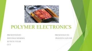
POLYMER ELECTRONICS 
PRESENTED BY: PRESENTED TO: 
SHIVANGI SHARMA PRAVEEN JAIN SIR 
M.TECH 1YEAR 
CCT 
1
WHAT IS POLYMER ELECTRONICS? 
 Polymers are long-chain molecules consisting of many repeat units 
to make a solid material. 
 Polymers are normally electrical insulators, but to enable their use in 
electronics, conductive filler such as silver have been added to 
chemical formulation to increase their electrical conductivity. 
 The merits in this research area, the Nobel Prize 2000 for Chemistry 
was awarded to Alan J. Heeger, Alan G. MacDiarmid und Hideki 
Shirakawa. 
2
WHAT MAKES POLYMER SO SUITABLE 
FOR ELECTRONICS APPLICATION? 
 Good insulator of heat 
 Can form any shape. 
 They have low density 
 They require low finishing cost. 
 Their toughness and ductility is good 
 Enhanced flexibility allowed for many application. 
 Solubility in organic solvents, variable processibility. 
3
ELECTRIC CONDUCTOR POLYMER TYPES 
 Depending on the type of charge transport by the carriers responsible for it 
 Ionically conductive polymer: 
It is used as a solid-state electrolyte in batteries. 
Eg: poly ethylene oxide which contain lithium perchlorate(LiClO4). 
 Electronically conductive: 
1. Filled conductive polymers 
2. Intrinsically conductive polymers 
4
INTRINSICALLY CONDUCTIVE POLYMER 
 They do not incorporate any conductive additives. 
 They gain their electrical Conductivity through a property known 
as ‘conjugation’. 
 Conjugated polymers are doped with atoms that donate negative 
or positive charges enabling current to travel down the polymer 
chain. 
5
TWO CONDITIONS TO BECOME CONDUCTIVE 
1. The first condition is the polymer consists of alternating single and double 
bonds, called conjugated double bonds. 
 In conjugation, the bonds between the carbon atoms are alternately single 
and double. Every bond contains a localised “sigma” (σ) bond which forms 
a strong chemical bond. In addition, every double bond also contains a less 
strongly localised “pi” (π) bond which is weaker. 
6
Contd… 
2. The second condition is the plastic has to be disturbed - either by 
removing electrons from (oxidation), or inserting them into 
(reduction), the material. The process is known as Doping. 
There are two types of doping: 
 Oxidation with halogen (or p-doping). 
 Reduction with alkali metal (called n-doping). 
7
ICP MATERIAL 
 Polyaniline 
 Polythiophene 
 Polypyrrole 
 Polyacetylene 
8
PROPERTIES OF ICP 
 Electrical conductivity 
 Ability to store an electric charge 
 Ability to exchange ions 
9
ICP AS A MATRIX POLYMER 
 It provide design flexibility, good filler incorporation-ability, specific 
interactions with fillers and microwave non-transparency. 
10
ELECTRICAL PROPERTIES OF ICP BASED 
NANOCOMPOSITES 
Variation of electrical conductivity (ln σdc) of hydrochloric acid (HCl) doped Emeraldine 
base (EB) samples as a function of dopant (HCl) concentration (a) 0.0 M (b) 0.001 M, (c) 0.01 M, (d) 0.1 
11 
M, (e) 0.3 M, (f) 0.5 M, (g) 0.7 M, (h) 0.9 M and (i) 1.0 M
APPLICATION 
 Fabrication of organic thin film transistors 
 Non-volatile memory devices based on organic transistors 
 Development of novel conjugated polymers for photovoltaic 
device applications 
 Fabrication of organic photovoltaic cells 
 Fabrication of organic light-emitting devices (OLED) 
 Ferroelectric polymers for thin film devices 
 Gene Sensors 
 Printed Electronics 
 Conducting Polymer Actuators and Micropumps. 
 Responsive Membranes/Hybrid Plastics. 
 focused upon polymer membranes that incorporated 
electronically conducting polymers and piezoelectric polymers 
12
PRINTED ELECTRONICS 
 It is a set of printing methods used to 
create electrical devices on various 
substract. 
 Printed electronics, specifies the process 
and subject to the specific requirements 
of the printing process selected can 
utilize any solution-based material. 
 This includes organic semiconductors, 
inorganic semiconductors, metallic 
conductors, nanoparticles, nanotubes, 
etc. 
13
PRINTED ELECTRONICS METHODS 
 Flexo printing: a high pressure method that is especially well 
applicable to print on plastic substrates 
 Offset printing: a flat printing technique that makes a high resolution 
possible 
 Gravure printing: a low pressure printing method that makes high 
volumes and the use of organic dissolvent possible 
 Rotary screen printing: a method that allows to print in thick layers 
14
ORGANIC THIN FILM TRANSISTOR 
 They use organic molecules rather than silicon for their active 
material. This active material may be composed of avoide varity 
of molecules. 
 ADVANTAGES 
• Compatibility with plastic substance. 
• Lower cost deposition process such as spin coating, printing, 
evaporation, 
• Lower temperature manufacturing(60-120c) 
 DISADVANTAGES 
• Lower mobility and switching speed compared to silicon wafers. 
15
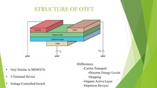
STRUCTURE OF OTFT 
•Differences 
–Carrier Transport 
•Discrete Energy Levels 
•Hopping 
–Organic Active Layer 
–Depletion Devices 
• Very Similar to MOSFETs 
• 3-Terminal Device 
• Voltage Controlled Switch 
16
APPLICATION OF ORGANIC TFT 
Organic Thin Film 
Transistor 
OLED Device 
Liquid Crystal 
Device 
E-ink 
Antenna 
Materials 
Integration 
Technology 
OLED Display 
Plastic TFT LCD 
E-paper, E-book 
Contactless Smart 
Card 
Wearable 
Computer 
17
ADVANTAGES V/S DISADVANTAGES OF 
POLYMER ELECTRONICS 
ADVANTAGES 
• Manufacture is relative simple and 
inexpensive equipment at low cost. 
• Light weighted and flexible, very 
durable under stress and flex can 
be easily applied over a large 
surface area. 
• Freedom of choice of their 
chemical composition 
• Adaptable in various ways 
because of printing methods that 
can be adjusted to current 
requirements quickly (printed 
electronics) 
DISADVANTAGES 
• Due to their intrinsic physical properties 
(i.e. limited mobility of charge carriers), 
the performance of polymer electronic 
products lacks the speed of its silicon 
counterpart. 
• Research is still on going to increase 
performance for more complex 
functionality. 
• To be able to improve performance one 
should be able to distinguish between 
problems introduced during preparation, 
intrinsic material properties, and device 
18 
characteristics
CONCLUSION 
 ICPs are Electrically-conductive polymers in which the Conductivity 
arises from the presence of conjugated car-bon-carbon bonds. These 
conjugated polymers possess interesting and useful properties due to their 
delocalised electron systems. 
 Polymer electronics are light, flexible, and less expensive to produce on a 
mass quantity scale than conventional electronics 
 Polymer electronics are not a competing product but are considered to 
be more complementary to its silicon counterpart. 
19

Polymer electronics

  • 1.
    POLYMER ELECTRONICS PRESENTEDBY: PRESENTED TO: SHIVANGI SHARMA PRAVEEN JAIN SIR M.TECH 1YEAR CCT 1
  • 2.
    WHAT IS POLYMERELECTRONICS?  Polymers are long-chain molecules consisting of many repeat units to make a solid material.  Polymers are normally electrical insulators, but to enable their use in electronics, conductive filler such as silver have been added to chemical formulation to increase their electrical conductivity.  The merits in this research area, the Nobel Prize 2000 for Chemistry was awarded to Alan J. Heeger, Alan G. MacDiarmid und Hideki Shirakawa. 2
  • 3.
    WHAT MAKES POLYMERSO SUITABLE FOR ELECTRONICS APPLICATION?  Good insulator of heat  Can form any shape.  They have low density  They require low finishing cost.  Their toughness and ductility is good  Enhanced flexibility allowed for many application.  Solubility in organic solvents, variable processibility. 3
  • 4.
    ELECTRIC CONDUCTOR POLYMERTYPES  Depending on the type of charge transport by the carriers responsible for it  Ionically conductive polymer: It is used as a solid-state electrolyte in batteries. Eg: poly ethylene oxide which contain lithium perchlorate(LiClO4).  Electronically conductive: 1. Filled conductive polymers 2. Intrinsically conductive polymers 4
  • 5.
    INTRINSICALLY CONDUCTIVE POLYMER  They do not incorporate any conductive additives.  They gain their electrical Conductivity through a property known as ‘conjugation’.  Conjugated polymers are doped with atoms that donate negative or positive charges enabling current to travel down the polymer chain. 5
  • 6.
    TWO CONDITIONS TOBECOME CONDUCTIVE 1. The first condition is the polymer consists of alternating single and double bonds, called conjugated double bonds.  In conjugation, the bonds between the carbon atoms are alternately single and double. Every bond contains a localised “sigma” (σ) bond which forms a strong chemical bond. In addition, every double bond also contains a less strongly localised “pi” (π) bond which is weaker. 6
  • 7.
    Contd… 2. Thesecond condition is the plastic has to be disturbed - either by removing electrons from (oxidation), or inserting them into (reduction), the material. The process is known as Doping. There are two types of doping:  Oxidation with halogen (or p-doping).  Reduction with alkali metal (called n-doping). 7
  • 8.
    ICP MATERIAL Polyaniline  Polythiophene  Polypyrrole  Polyacetylene 8
  • 9.
    PROPERTIES OF ICP  Electrical conductivity  Ability to store an electric charge  Ability to exchange ions 9
  • 10.
    ICP AS AMATRIX POLYMER  It provide design flexibility, good filler incorporation-ability, specific interactions with fillers and microwave non-transparency. 10
  • 11.
    ELECTRICAL PROPERTIES OFICP BASED NANOCOMPOSITES Variation of electrical conductivity (ln σdc) of hydrochloric acid (HCl) doped Emeraldine base (EB) samples as a function of dopant (HCl) concentration (a) 0.0 M (b) 0.001 M, (c) 0.01 M, (d) 0.1 11 M, (e) 0.3 M, (f) 0.5 M, (g) 0.7 M, (h) 0.9 M and (i) 1.0 M
  • 12.
    APPLICATION  Fabricationof organic thin film transistors  Non-volatile memory devices based on organic transistors  Development of novel conjugated polymers for photovoltaic device applications  Fabrication of organic photovoltaic cells  Fabrication of organic light-emitting devices (OLED)  Ferroelectric polymers for thin film devices  Gene Sensors  Printed Electronics  Conducting Polymer Actuators and Micropumps.  Responsive Membranes/Hybrid Plastics.  focused upon polymer membranes that incorporated electronically conducting polymers and piezoelectric polymers 12
  • 13.
    PRINTED ELECTRONICS It is a set of printing methods used to create electrical devices on various substract.  Printed electronics, specifies the process and subject to the specific requirements of the printing process selected can utilize any solution-based material.  This includes organic semiconductors, inorganic semiconductors, metallic conductors, nanoparticles, nanotubes, etc. 13
  • 14.
    PRINTED ELECTRONICS METHODS  Flexo printing: a high pressure method that is especially well applicable to print on plastic substrates  Offset printing: a flat printing technique that makes a high resolution possible  Gravure printing: a low pressure printing method that makes high volumes and the use of organic dissolvent possible  Rotary screen printing: a method that allows to print in thick layers 14
  • 15.
    ORGANIC THIN FILMTRANSISTOR  They use organic molecules rather than silicon for their active material. This active material may be composed of avoide varity of molecules.  ADVANTAGES • Compatibility with plastic substance. • Lower cost deposition process such as spin coating, printing, evaporation, • Lower temperature manufacturing(60-120c)  DISADVANTAGES • Lower mobility and switching speed compared to silicon wafers. 15
  • 16.
    STRUCTURE OF OTFT •Differences –Carrier Transport •Discrete Energy Levels •Hopping –Organic Active Layer –Depletion Devices • Very Similar to MOSFETs • 3-Terminal Device • Voltage Controlled Switch 16
  • 17.
    APPLICATION OF ORGANICTFT Organic Thin Film Transistor OLED Device Liquid Crystal Device E-ink Antenna Materials Integration Technology OLED Display Plastic TFT LCD E-paper, E-book Contactless Smart Card Wearable Computer 17
  • 18.
    ADVANTAGES V/S DISADVANTAGESOF POLYMER ELECTRONICS ADVANTAGES • Manufacture is relative simple and inexpensive equipment at low cost. • Light weighted and flexible, very durable under stress and flex can be easily applied over a large surface area. • Freedom of choice of their chemical composition • Adaptable in various ways because of printing methods that can be adjusted to current requirements quickly (printed electronics) DISADVANTAGES • Due to their intrinsic physical properties (i.e. limited mobility of charge carriers), the performance of polymer electronic products lacks the speed of its silicon counterpart. • Research is still on going to increase performance for more complex functionality. • To be able to improve performance one should be able to distinguish between problems introduced during preparation, intrinsic material properties, and device 18 characteristics
  • 19.
    CONCLUSION  ICPsare Electrically-conductive polymers in which the Conductivity arises from the presence of conjugated car-bon-carbon bonds. These conjugated polymers possess interesting and useful properties due to their delocalised electron systems.  Polymer electronics are light, flexible, and less expensive to produce on a mass quantity scale than conventional electronics  Polymer electronics are not a competing product but are considered to be more complementary to its silicon counterpart. 19

Editor's Notes

  • #6 Conjugation means polymer molecules have alternating double and single bonds.which provide pathway to free electron.conjugated polymer can be doped.doping in polymer is carried out with oxidizing or reducing agent that remove or add e- to the polymer.this oxidation and reduction changes the electronic structure to 1 that will conduct electricity.the addition of even very small amount of dopants can cause a major change in bulk material’s property
  • #8 Conjugation means polymer molecules have alternating double and single bonds.which provide pathway to free electron.conjugated polymer can be doped.doping in polymer is carried out with oxidizing or reducing agent that remove or add e- to the polymer.this oxidation and reduction changes the electronic structure to 1 that will conduct electricity.the addition of even very small amount of dopants can cause a major change in bulk material’s property
  • #10 onducting polymers appear to be one of the few materials capable of displaying dynamic (switchable) microwave absorption behavior, which are called “intelligent stealth materials”, due to the reversible electrical properties of conducting polymers affected by redox doping/de-doping processes.