Downloaded 200 times


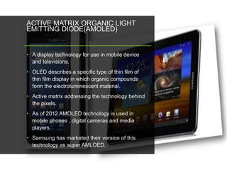
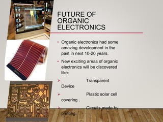


The document discusses organic electronics, focusing on conductive organic materials, their applications, advantages, and disadvantages compared to inorganic electronics. Key applications include organic light-emitting diodes (OLEDs), organic field-effect transistors (OFETs), and organic solar cells (OSCs), with an emphasis on their flexibility, low cost, and potential future developments. The conclusion highlights the increasing demand for organic electronics due to their diverse applications and innovative features.


![OPV INTRODUCTION.pptx [Autoservved].pptx](https://cdn.slidesharecdn.com/ss_thumbnails/opvintroduction-250808125729-4ef4caea-thumbnail.jpg?width=640&height=640&fit=bounds)


![[Marco mazzeo] organic_light_emitting_diode(book_zz.org)](https://cdn.slidesharecdn.com/ss_thumbnails/marcomazzeoorganiclightemittingdiodebookzz-150114151251-conversion-gate01-thumbnail.jpg?width=640&height=640&fit=bounds)


![Attack surfaces and attack tress[inform]](https://cdn.slidesharecdn.com/ss_thumbnails/lecture03-260108015941-a4dee53b-thumbnail.jpg?width=640&height=640&fit=bounds)
