Specifications
The vendor orclient provide the specifications like
High performance
Area
Low power consumption
Low cost
4.
Architecture
According to specificationswe built blue print of chip
All details on proccessors,memories&how they are connected
How much block area is used &how much cost required and how much power
consumed
5.
Rtl coding
Base onarchitecture we will write rtl code
We build digital design of seqt ckts&comb ckts by using Hdl,vhdl,Verilog,system
Verilog
6.
Rtl simulation
Functional verificationis done in this process
Aftr rtl design we apply test cases in verification stage
Test cases are called behavioural simulations such as NC SIM,TOGGLE COVERAGE
7.
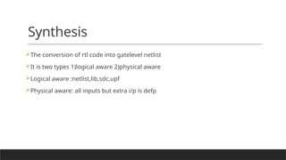
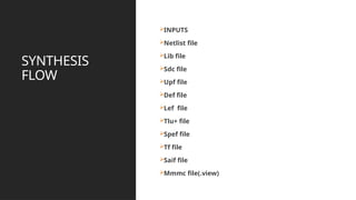
Synthesis
The conversion ofrtl code into gatelevel netlist
It is two types 1)logical aware 2)physical aware
Logical aware :netlist,lib,sdc,upf
Physical aware: all inputs but extra i/p is defp
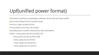
Upf(unified power format)
ifthe block is working on multivoltage,multipower domain then we require upf file
Upf consists of power info of complete design
There are 2 types of power format
Primary power ( core rings ,rails, stripes)
Secondary power ( isolation cells,retention cells, level shifters)
Syntax – create_power_domain_PD_ORCA_TOP
create_power_domain_PD_RISC_CORE
create_supply_net_vss_domain
create_supply_net_vdd_domain
create_supply_port_vss_domain
15.
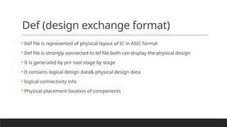
Def (design exchangeformat)
Def file is represented of physical layout of IC in ASIC format
Def file is strongly connected to lef file,both can display the physical design
It is generated by pnr tool stage by stage
It contains logical design data& physical design data
logical-connectivity info
Physical-placement location of components
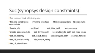
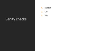
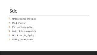
Sdc
1. Unconstrained endpoints
2.I/p & o/p delay
3. Port io missing delay
4. Multi clk driven registers
5. No clk reaching flipflop
6. Linking related issues
20.
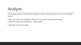
Analyze
In analyze stageit will read all required inputs,check the syntax errors for loaded
inputs
Here the tool read Verilog & check for any syntax errors like missing
modules,unreserve references , black boxes
#Analyze_format_Verilog
21.
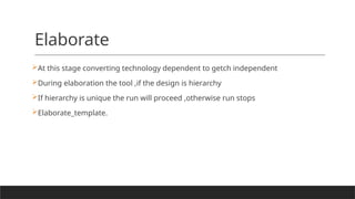
Elaborate
At this stageconverting technology dependent to getch independent
During elaboration the tool ,if the design is hierarchy
If hierarchy is unique the run will proceed ,otherwise run stops
Elaborate_template.
22.
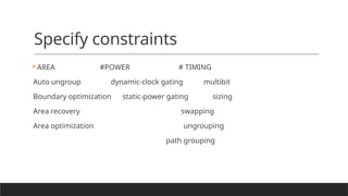
Specify constraints
AREA #POWER# TIMING
Auto ungroup dynamic-clock gating multibit
Boundary optimization static-power gating sizing
Area recovery swapping
Area optimization ungrouping
path grouping
Compile
It is usedto check sematic errors from top of flow to bottom of flow
25.
Insert Dft(design fortesting)
At this stage we will add logic to the design,to check functionality the block
26.
Compile Ultra incrementals
Atthis stage before it will check errors stage by stage
In ultra incrementals stage its resume process from copile ultra incremental stage
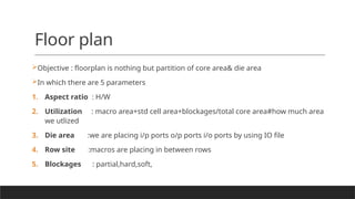
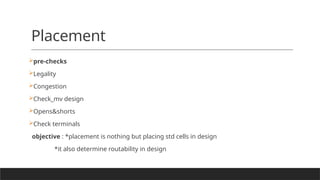
Floor plan
Objective :floorplan is nothing but partition of core area& die area
In which there are 5 parameters
1. Aspect ratio : H/W
2. Utilization : macro area+std cell area+blockages/total core area#how much area
we utlized
3. Die area :we are placing i/p ports o/p ports i/o ports by using IO file
4. Row site :macros are placing in between rows
5. Blockages : partial,hard,soft,
31.
Inputs :
All inputs,IO file
Outputs :
Floordef
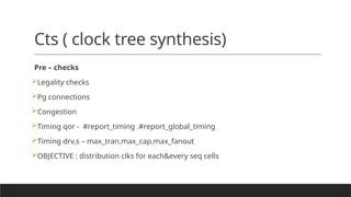
pre - checks
We should see no over laps of macros&ports
Check proper offset of ports
32.
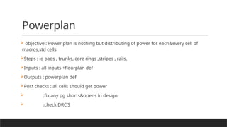
Powerplan
objective :Power plan is nothing but distributing of power for each&every cell of
macros,std cells
Steps : io pads , trunks, core rings ,stripes , rails,
Inputs : all inputs +floorplan def
Outputs : powerplan def
Post checks : all cells should get power
:fix any pg shorts&opens in design
:check DRC’S
33.
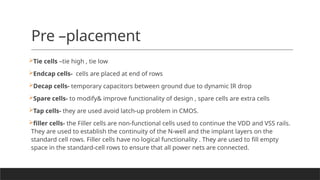
Pre –placement
Tie cells–tie high , tie low
Endcap cells- cells are placed at end of rows
Decap cells- temporary capacitors between ground due to dynamic IR drop
Spare cells- to modify& improve functionality of design , spare cells are extra cells
Tap cells- they are used avoid latch-up problem in CMOS.
filler cells- the Filler cells are non-functional cells used to continue the VDD and VSS rails.
They are used to establish the continuity of the N-well and the implant layers on the
standard cell rows. Filler cells have no logical functionality . They are used to fill empty
space in the standard-cell rows to ensure that all power nets are connected.
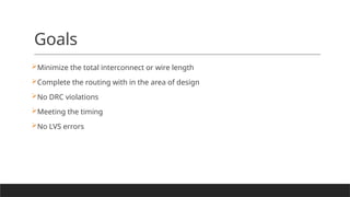
Goals
Minimize the totalinterconnect or wire length
Complete the routing with in the area of design
No DRC violations
Meeting the timing
No LVS errors