What is a PCBA
•
1 like•158 views

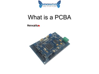
PCBA is the abbreviation of Printed Circuit Board Assembly, which means that the PCB blank board passes the SMT upper part, or the whole process of DIP plug-in, referred to as PCBA.

Recommended
More Related Content
What's hot
What's hot (20)
Similar to What is a PCBA
Similar to What is a PCBA (20)
More from Luna Leng
More from Luna Leng (7)
Recently uploaded
Recently uploaded (20)
What is a PCBA
- 1. What is a PCBA
- 2. Introduction PCBA is the abbreviation of Printed Circuit Board Assembly, which means that the PCB blank board passes the SMT upper part, or the whole process of DIP plug-in, referred to as PCBA. Pcb-dayee.com
- 3. Where Does PCBA Comes From Printed circuit boards, also known as PCB (Printed circuit board), is an important electronic component, it is the supporter of electronic components, and it is also the provider of electronic components line connection. Because it is made using electronic printing technology, it is called a "printing" circuit board. Prior to the advent of printed circuit boards, the interconnection between electronic components relied on wires to form a complete line. Today, circuit breadboards exist only as an effective experimental tool, and printed circuit boards have become the dominant position in the electronics industry. At the beginning of the 20th century, in order to simplify the production of electronic devices, reduce the wiring between electronic components, and reduce the manufacturing cost, the method of replacing wiring by printing was started. For thirty years, engineers have been proposing to wire metal conductors on insulated substrates. The most successful is that in 1925, the United States Charles Ducas printed a circuit pattern on an insulated substrate, and then successfully established a conductor for wiring by electroplating. Pcb-dayee.com
- 4. Where Does PCBA Comes From Until 1936, the Austrian Paul Eisler published foil technology in the UK, he used a printed circuit board in a radio device; in Japan, Miyamoto Hiroyuki sprayed wiring The law "small method of blowing the wiring method (license 119384)" successfully applied for a patent. In the two, Paul Eisler's method is most similar to today's printed circuit boards. This type of practice is called subtraction, which removes unwanted metals. Charles Ducas and Miyamoto's approach is only added. The wiring required is called the additive method. Even so, because the electronic components at that time generated a large amount of heat, the substrates of the two were difficult to use, so that there was no formal use, but the printed circuit technology was further improved. Pcb-dayee.com
- 5. PCB & PCBA development In 1941, the United States painted copper paste on talc for wiring to make a proximity tube. In 1943, Americans used the technology extensively in military radios. In 1947, epoxy resins began to be used as substrates for fabrication. At the same time, NBS began to study the manufacturing technology of coils, capacitors, resistors, etc. by printed circuit technology. In 1948, the United States officially recognized the invention for commercial use. Since the 1950s, transistors with lower heat generation have largely replaced the status of vacuum tubes, and printed circuit board technology has only begun to be widely adopted. At that time, the etched foil technology was the mainstream. In 1950, in Japan, silver lacquer was used as a wiring on a glass substrate, and copper foil was used as a wiring on a paper phenolic substrate (CCL) made of a phenol resin. In 1951, the appearance of polyimide made the heat resistance of the resin further, and a polyimide substrate was also produced. Pcb-dayee.com
- 6. PCB & PCBA development In 1941, the United States painted copper paste on talc for wiring to make a proximity tube. In 1943, Americans used the technology extensively in military radios. In 1947, epoxy resins began to be used as substrates for fabrication. At the same time, NBS began to study the manufacturing technology of coils, capacitors, resistors, etc. by printed circuit technology. In 1948, the United States officially recognized the invention for commercial use. Since the 1950s, transistors with lower heat generation have largely replaced the status of vacuum tubes, and printed circuit board technology has only begun to be widely adopted. At that time, the etched foil technology was the mainstream. In 1950, in Japan, silver lacquer was used as a wiring on a glass substrate, and copper foil was used as a wiring on a paper phenolic substrate (CCL) made of a phenol resin. In 1951, the appearance of polyimide made the heat resistance of the resin further, and a polyimide substrate was also produced. Pcb-dayee.com
- 7. PCB & PCBA development In 1941, the United States painted copper paste on talc for wiring to make a proximity tube. In 1943, Americans used the technology extensively in military radios. In 1947, epoxy resins began to be used as substrates for fabrication. At the same time, NBS began to study the manufacturing technology of coils, capacitors, resistors, etc. by printed circuit technology. In 1948, the United States officially recognized the invention for commercial use. Since the 1950s, transistors with lower heat generation have largely replaced the status of vacuum tubes, and printed circuit board technology has only begun to be widely adopted. At that time, the etched foil technology was the mainstream. In 1950, in Japan, silver lacquer was used as a wiring on a glass substrate, and copper foil was used as a wiring on a paper phenolic substrate (CCL) made of a phenol resin. In 1951, the appearance of polyimide made the heat resistance of the resin further, and a polyimide substrate was also produced. Pcb-dayee.com
- 8. PCBA Practical In the late 1990s, when a number of build-up printed circuit board solutions were proposed, the build-up printed circuit boards were officially and largely put into practical use until now. It is important to develop a robust test strategy for large, high-density printed circuit board assemblies (PCBA) to ensure compliance and functionality. In addition to the establishment and testing of these complex assemblies, the amount of money invested in electronic components can be very high - up to $25,000 when a unit is tested. Because of this high cost, the problem of finding and repairing assemblies is now even more important than in the past. Today's more complex assembly is approximately 18 square inches, 18 layers; there are more than 2,900 components on the top and bottom; 6,000 circuit nodes; more than 20,000 solder joints to be tested. In 1953, Motorola developed a double panel with a plated through hole method. This method is also applied to later multilayer boards. Printed circuit boards were widely used 10 years later in the 1960s, and their technology is becoming more mature. Since the introduction of Motorola's dual- panel, multi-layer printed circuit boards have begun to appear, increasing the ratio of wiring to substrate area. Pcb-dayee.com
- 9. PCBA Practical In 1960, V. Dahlgreen applied a circuit-coated metal foil film to a thermoplastic plastic to create a flexible printed circuit board. In 1961, Hazeltine Corporation of the United States made a multi-layer board by referring to the plated through-hole method. In 1967, "Plated-up technology", one of the method of layering, was published.[3] In 1969, FD-R made flexible printed circuit boards from polyimide. In 1979, Pactel published the "Pactel Method", one of the methods of layering. In 1984, NTT developed the "Copper Polyimide Method" for thin film circuits. In 1988, Siemens developed the multilayer printed circuit board of Microwiring Substrate. In 1990, IBM developed a layered printed circuit board for the Surface Laminar Circuit (SLC). In 1995, Matsushita Electric developed a layered printed circuit board for ALIVH. In 1996, Toshiba developed a B2it build-up printed circuit board. Pcb-dayee.com
- 10. Bare-board test Boards with no components installed are usually bare-board tested for "shorts" and "opens". A short is a connection between two points that should not be connected. An open is a missing connection between points that should be connected. For high-volume production, a fixture or a rigid needle adapter makes contact with copper lands on the board. The fixture or adapter is a significant fixed cost and this method is only economical for high-volume or high-value production. For small or medium volume production flying probe testers are used where test probes are moved over the board by an XY drive to make contact with the copper lands. There is no need for a fixture and hence the fixed costs are much lower. The CAM system instructs the electrical tester to apply a voltage to each contact point as required and to check that this voltage appears on the appropriate contact points and only on these. Pcb-dayee.com
- 11. PCB Assembly In assembly the bare board is populated (or "stuffed") with electronic components to form a functional printed circuit assembly (PCA), sometimes called a "printed circuit board assembly" (PCBA). In through-hole technology, the component leads are inserted in holes surrounded by conductive pads; the holes keep the components in place. In surface-mount technology (SMT), the component is placed on the PCB so that the pins line up with the conductive pads or lands on the surfaces of the PCB; solder paste, which was previously applied to the pads, holds the components in place temporarily; if surface-mount components are applied to both sides of the board, the bottom-side components are glued to the board. In both through hole and surface mount, the components are then soldered; once cooled and solidified, the solder holds the components in place permanently and electrically connects them to the board. Pcb-dayee.com
- 12. About Hengkaituo’s PCB Assembly HENGKATITUO PCBA business was started in 2004, which specializes in ONE STOP OEM & ODM PCB assembly full turnkey services. If you are ready to have your design manufactured, please send your files to email: sales1@pcb- dayee.com for quote. File formats: Gerber file: CAM350 RS274X OR PCB file: Protel 99SE, P-CAD 2001 PCB BOM: Excel (PDF,word,txt) Or if you want more information on prototype circuit board assembly or design keys to aid your needs in the PCBA process, contact us. Shenzhen Hengkaituo Sci-tech CO., LTD Email: sales1@pcb-dayee.com Wechat: janema6 Skype: dayeeservice QQ: 1059092587 Website: https://www.pcb-dayee.com/ Pcb-dayee.com