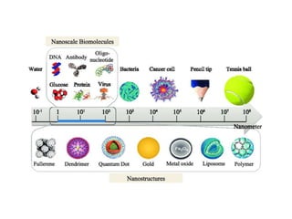
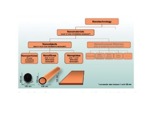
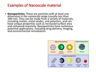
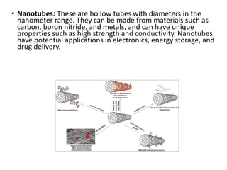
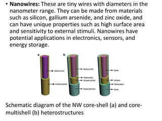
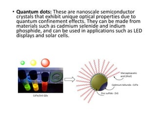
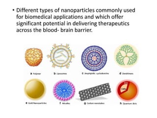
NANOSCALE
~Jayati Shrivastava
What is nanoscale?
• The nanoscale refers to a length scale between
approximately 1 and 100 nanometers (nm).
• At the nanoscale, materials and structures exhibit
unique properties and behaviors that differ from
those at larger scales.
What is Nanotechnology?
• Nanotechnology involves the design, fabrication, and
manipulation of materials and devices at the nanoscale.
• The nanoscale refers to a length scale between approximately 1
and 100 nanometers (nm).
• At the nanoscale, materials and structures exhibit unique
properties and behaviors that differ from those at larger scales.
• Nanotechnology has numerous potential applications in fields
such as medicine, electronics, energy, and environmental
remediation.
• At the nanoscale, materials exhibit unique
properties and behaviors that differ from those at
larger scales, which can be harnessed for various
applications
Nanoscale Technology
• Nanoscale technology involves the design, fabrication,
and characterization of materials and structures at the
nanoscale.
• The development of nanoscale technology has been
enabled by advances in fields such as materials science,
chemistry, and physics.
• The study of the nanoscale is interdisciplinary, involving
a range of fields including biology, physics, chemistry,
and engineering.
Tools and Techniques involved in Nanoscale
Technology.
• Scanning Probe Microscopy (SPM): SPM is a family of
techniques that use a physical probe to scan a sample
surface and generate a high-resolution image. Examples
of SPM techniques include Atomic Force Microscopy
(AFM) and Scanning Tunneling Microscopy (STM).
• Electron Microscopy: Electron microscopy techniques use
beams of electrons to image and analyze samples at the
nanoscale. Examples include Transmission Electron
Microscopy (TEM) and Scanning Electron Microscopy
(SEM).
• X-ray Diffraction (XRD): XRD is a technique that
uses X-rays to determine the atomic and molecular
structure of materials. This is useful for
characterizing the crystal structure of
nanomaterials.
• Nanolithography: Nanolithography is the process
of creating nanoscale patterns and structures on a
surface. Examples of nanolithography techniques
include Electron Beam Lithography (EBL) and
Nanoimprint Lithography (NIL).
• Molecular Self-Assembly: Molecular self-assembly is a process
where molecules spontaneously organize themselves into ordered
structures. This technique can be used to create nanoscale
structures and devices.
• Chemical Vapor Deposition (CVD): CVD is a technique where a gas
or vapor is deposited on a substrate to create a thin film. This
technique can be used to create nanomaterials with specific
properties.
• Nanomanipulation: Nanomanipulation involves manipulating and
positioning individual atoms or molecules using specialized tools.
Examples of nanomanipulation techniques include Scanning Probe
Microscopy-based nanomanipulation and Optical Tweezers.
Properties of Nanoscale
• Size: Nanoscale materials are typically between 1
and 100 nanometers in size, which is much smaller
than the wavelength of visible light. This small size
gives them unique properties compared to bulk
materials.
• Surface area: Because of their small size, nanoscale
materials have a high surface area to volume ratio,
which can lead to enhanced reactivity and
increased surface energy.
• Mechanical properties: Nanoscale materials can
exhibit enhanced strength, flexibility, and hardness
compared to bulk materials.
• Thermal properties: Nanoscale materials can exhibit
enhanced thermal conductivity and heat dissipation
due to their small size and high surface area.
• Electrical properties: Nanoscale materials can
exhibit unique electrical properties, such as
increased conductivity, tunable band gaps, and
enhanced charge transfer.
• Optical properties: Nanoscale materials can exhibit
unique optical properties, such as plasmonic
resonance, which can be harnessed for various
applications in optics and photonics.
• Chemical properties: Nanoscale materials can exhibit
enhanced chemical reactivity, which can be used for
various applications such as catalysis and sensing.
• Magnetic properties: Nanoscale materials can exhibit
unique magnetic properties, such as
superparamagnetism and ferromagnetism, which can
be useful for applications such as data storage and
magnetic resonance imaging (MRI).
• Quantum effects: At the nanoscale, materials
exhibit quantum effects such as quantum
confinement and the quantum size effect, which
can cause changes in their optical, electronic, and
magnetic properties.
Biological properties: Nanoscale materials can
interact with biological systems in unique ways, which
can be useful for applications such as drug delivery
and biosensing.
Examples of Nanoscale material
• Nanoparticles: These are particles with at least one
dimension in the nanoscale range (usually less than
100 nm). They can be made from a variety of materials,
including metals, metal oxides, and polymers, and can
have unique properties such as increased surface area
and enhanced reactivity. Nanoparticles have numerous
potential applications, including drug delivery, imaging,
and environmental remediation.
• Nanotubes: These are hollow tubes with diameters in the
nanometer range. They can be made from materials such as
carbon, boron nitride, and metals, and can have unique
properties such as high strength and conductivity. Nanotubes
have potential applications in electronics, energy storage, and
drug delivery.
• Nanowires: These are tiny wires with diameters in the
nanometer range. They can be made from materials
such as silicon, gallium arsenide, and zinc oxide, and
can have unique properties such as high surface area
and sensitivity to external stimuli. Nanowires have
potential applications in electronics, sensors, and
energy storage.
Schematic diagram of the NW core-shell (a) and core-
multishell (b) heterostructures
• Quantum dots: These are nanoscale semiconductor
crystals that exhibit unique optical properties due to
quantum confinement effects. They can be made from
materials such as cadmium selenide and indium
phosphide, and can be used in applications such as LED
displays and solar cells.
Nanoscale materials in biological systems:
• Biological structures: Many biological structures, such as
proteins, DNA, and viruses, are nanoscale in size and exhibit
unique properties at this scale.
• Cell interactions: Nanoscale materials can interact with cells and
tissues in unique ways, such as crossing cell membranes or
adhering to cell surfaces, which can be harnessed for various
biomedical applications.
• Drug delivery: Nanoscale materials can be engineered to deliver
drugs and therapeutic agents directly to targeted cells and
tissues, improving drug efficacy and reducing side effects.
• Imaging: Nanoscale materials can be used as contrast agents for
various imaging techniques such as magnetic resonance imaging
(MRI), computed tomography (CT), and fluorescence imaging,
allowing for improved visualization of tissues and diseases.
• Sensors and diagnostics: Nanoscale materials can be used as
biosensors for the detection of biological molecules and
pathogens, as well as for the diagnosis of diseases.
• Tissue engineering: Nanoscale materials can be used in tissue
engineering applications to create scaffolds that promote cell
growth and tissue regeneration.
• Toxicity: The unique properties of nanoscale materials can also
raise concerns regarding their potential toxicity in biological
systems.
Application of Nanoscale
• Electronics: Nanoscale materials are used in electronic
devices such as transistors, batteries, and sensors to
improve their performance and efficiency.
• Energy: Nanoscale materials are used in solar panels, fuel
cells, and energy storage devices to improve their efficiency
and reduce costs.
• Medicine: Nanoscale materials are used in drug delivery,
imaging, and diagnostic applications to improve the efficacy
and safety of medical treatments.
• Different types of nanoparticles commonly used
for biomedical applications and which offer
significant potential in delivering therapeutics
across the blood- brain barrier.
• Environmental remediation: Nanoscale materials are
used to remove pollutants from water and air, and to
improve the efficiency of waste treatment processes.
• Food and agriculture: Nanoscale materials are used in
food packaging, preservation, and safety, as well as in
agriculture to improve crop yield and disease
resistance.
• Materials science: Nanoscale materials are used in the
development of new materials with improved
properties such as strength, flexibility, and conductivity.

NANOSCALE.pdf

  • 1.
  • 2.
    What is nanoscale? •The nanoscale refers to a length scale between approximately 1 and 100 nanometers (nm). • At the nanoscale, materials and structures exhibit unique properties and behaviors that differ from those at larger scales.
  • 4.
    What is Nanotechnology? •Nanotechnology involves the design, fabrication, and manipulation of materials and devices at the nanoscale. • The nanoscale refers to a length scale between approximately 1 and 100 nanometers (nm). • At the nanoscale, materials and structures exhibit unique properties and behaviors that differ from those at larger scales. • Nanotechnology has numerous potential applications in fields such as medicine, electronics, energy, and environmental remediation.
  • 6.
    • At thenanoscale, materials exhibit unique properties and behaviors that differ from those at larger scales, which can be harnessed for various applications
  • 7.
    Nanoscale Technology • Nanoscaletechnology involves the design, fabrication, and characterization of materials and structures at the nanoscale. • The development of nanoscale technology has been enabled by advances in fields such as materials science, chemistry, and physics. • The study of the nanoscale is interdisciplinary, involving a range of fields including biology, physics, chemistry, and engineering.
  • 8.
    Tools and Techniquesinvolved in Nanoscale Technology. • Scanning Probe Microscopy (SPM): SPM is a family of techniques that use a physical probe to scan a sample surface and generate a high-resolution image. Examples of SPM techniques include Atomic Force Microscopy (AFM) and Scanning Tunneling Microscopy (STM). • Electron Microscopy: Electron microscopy techniques use beams of electrons to image and analyze samples at the nanoscale. Examples include Transmission Electron Microscopy (TEM) and Scanning Electron Microscopy (SEM).
  • 9.
    • X-ray Diffraction(XRD): XRD is a technique that uses X-rays to determine the atomic and molecular structure of materials. This is useful for characterizing the crystal structure of nanomaterials. • Nanolithography: Nanolithography is the process of creating nanoscale patterns and structures on a surface. Examples of nanolithography techniques include Electron Beam Lithography (EBL) and Nanoimprint Lithography (NIL).
  • 10.
    • Molecular Self-Assembly:Molecular self-assembly is a process where molecules spontaneously organize themselves into ordered structures. This technique can be used to create nanoscale structures and devices. • Chemical Vapor Deposition (CVD): CVD is a technique where a gas or vapor is deposited on a substrate to create a thin film. This technique can be used to create nanomaterials with specific properties. • Nanomanipulation: Nanomanipulation involves manipulating and positioning individual atoms or molecules using specialized tools. Examples of nanomanipulation techniques include Scanning Probe Microscopy-based nanomanipulation and Optical Tweezers.
  • 11.
    Properties of Nanoscale •Size: Nanoscale materials are typically between 1 and 100 nanometers in size, which is much smaller than the wavelength of visible light. This small size gives them unique properties compared to bulk materials. • Surface area: Because of their small size, nanoscale materials have a high surface area to volume ratio, which can lead to enhanced reactivity and increased surface energy.
  • 12.
    • Mechanical properties:Nanoscale materials can exhibit enhanced strength, flexibility, and hardness compared to bulk materials. • Thermal properties: Nanoscale materials can exhibit enhanced thermal conductivity and heat dissipation due to their small size and high surface area. • Electrical properties: Nanoscale materials can exhibit unique electrical properties, such as increased conductivity, tunable band gaps, and enhanced charge transfer.
  • 13.
    • Optical properties:Nanoscale materials can exhibit unique optical properties, such as plasmonic resonance, which can be harnessed for various applications in optics and photonics. • Chemical properties: Nanoscale materials can exhibit enhanced chemical reactivity, which can be used for various applications such as catalysis and sensing. • Magnetic properties: Nanoscale materials can exhibit unique magnetic properties, such as superparamagnetism and ferromagnetism, which can be useful for applications such as data storage and magnetic resonance imaging (MRI).
  • 14.
    • Quantum effects:At the nanoscale, materials exhibit quantum effects such as quantum confinement and the quantum size effect, which can cause changes in their optical, electronic, and magnetic properties. Biological properties: Nanoscale materials can interact with biological systems in unique ways, which can be useful for applications such as drug delivery and biosensing.
  • 15.
    Examples of Nanoscalematerial • Nanoparticles: These are particles with at least one dimension in the nanoscale range (usually less than 100 nm). They can be made from a variety of materials, including metals, metal oxides, and polymers, and can have unique properties such as increased surface area and enhanced reactivity. Nanoparticles have numerous potential applications, including drug delivery, imaging, and environmental remediation.
  • 16.
    • Nanotubes: Theseare hollow tubes with diameters in the nanometer range. They can be made from materials such as carbon, boron nitride, and metals, and can have unique properties such as high strength and conductivity. Nanotubes have potential applications in electronics, energy storage, and drug delivery.
  • 17.
    • Nanowires: Theseare tiny wires with diameters in the nanometer range. They can be made from materials such as silicon, gallium arsenide, and zinc oxide, and can have unique properties such as high surface area and sensitivity to external stimuli. Nanowires have potential applications in electronics, sensors, and energy storage. Schematic diagram of the NW core-shell (a) and core- multishell (b) heterostructures
  • 18.
    • Quantum dots:These are nanoscale semiconductor crystals that exhibit unique optical properties due to quantum confinement effects. They can be made from materials such as cadmium selenide and indium phosphide, and can be used in applications such as LED displays and solar cells.
  • 19.
    Nanoscale materials inbiological systems: • Biological structures: Many biological structures, such as proteins, DNA, and viruses, are nanoscale in size and exhibit unique properties at this scale. • Cell interactions: Nanoscale materials can interact with cells and tissues in unique ways, such as crossing cell membranes or adhering to cell surfaces, which can be harnessed for various biomedical applications. • Drug delivery: Nanoscale materials can be engineered to deliver drugs and therapeutic agents directly to targeted cells and tissues, improving drug efficacy and reducing side effects.
  • 20.
    • Imaging: Nanoscalematerials can be used as contrast agents for various imaging techniques such as magnetic resonance imaging (MRI), computed tomography (CT), and fluorescence imaging, allowing for improved visualization of tissues and diseases. • Sensors and diagnostics: Nanoscale materials can be used as biosensors for the detection of biological molecules and pathogens, as well as for the diagnosis of diseases. • Tissue engineering: Nanoscale materials can be used in tissue engineering applications to create scaffolds that promote cell growth and tissue regeneration. • Toxicity: The unique properties of nanoscale materials can also raise concerns regarding their potential toxicity in biological systems.
  • 21.
    Application of Nanoscale •Electronics: Nanoscale materials are used in electronic devices such as transistors, batteries, and sensors to improve their performance and efficiency. • Energy: Nanoscale materials are used in solar panels, fuel cells, and energy storage devices to improve their efficiency and reduce costs. • Medicine: Nanoscale materials are used in drug delivery, imaging, and diagnostic applications to improve the efficacy and safety of medical treatments.
  • 22.
    • Different typesof nanoparticles commonly used for biomedical applications and which offer significant potential in delivering therapeutics across the blood- brain barrier.
  • 23.
    • Environmental remediation:Nanoscale materials are used to remove pollutants from water and air, and to improve the efficiency of waste treatment processes. • Food and agriculture: Nanoscale materials are used in food packaging, preservation, and safety, as well as in agriculture to improve crop yield and disease resistance. • Materials science: Nanoscale materials are used in the development of new materials with improved properties such as strength, flexibility, and conductivity.