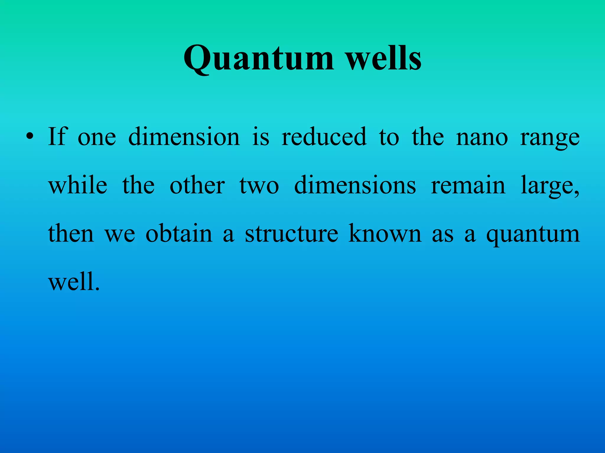
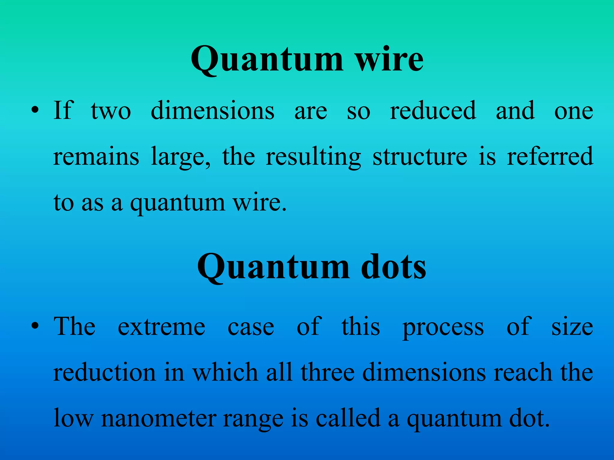
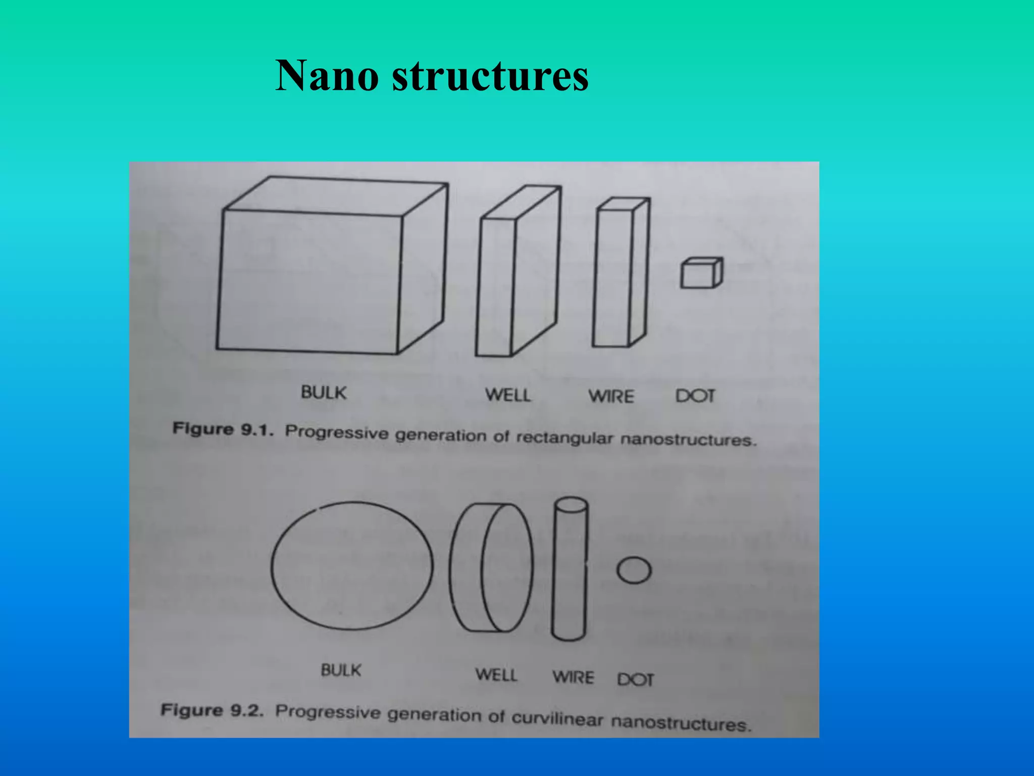
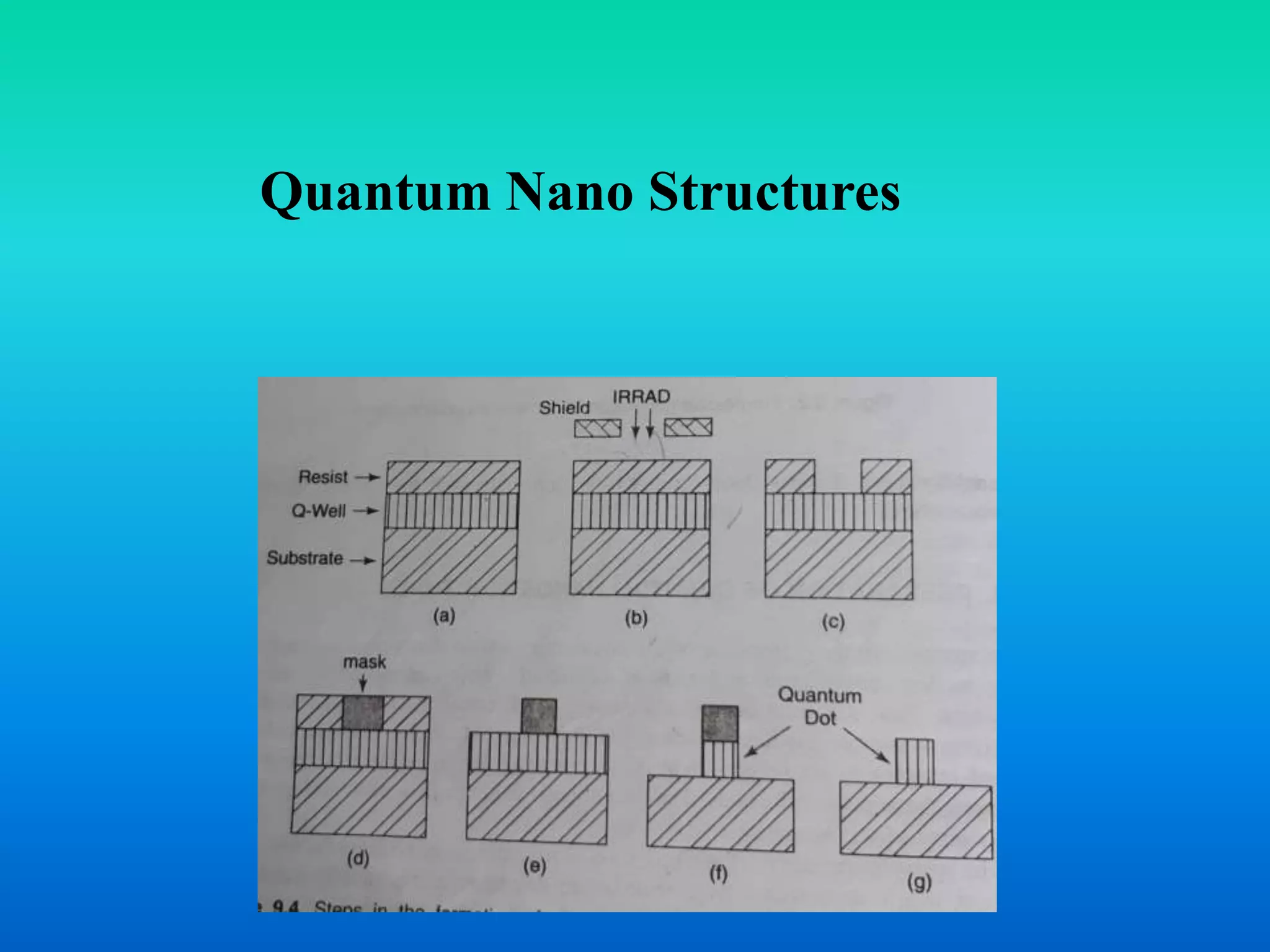
E.M.G. YADAVA WOMEN’S COLLEGE, MADURAI – 625 014.
(An Autonomous Institution – Affiliated to Madurai Kamaraj University)
Re-accredited (3rd Cycle) with Grade A+ and CGPA 3.51 by NAAC
NANO PHYSICS
TOPIC: Quantum Wells, Wires and Dots
By
Mrs. M.R. Gurulakshmi,
Department of physics,
Nano particles
• The size or dimension of a material is
continuously reduced from a large or macroscopic
size,
• such as a meter or a centimetres, to a very small
size,
• the properties remain the same at first then small
changes in properties can occur.
Quantum wells
• If one dimension is reduced to the nano range
while the other two dimensions remain large,
then we obtain a structure known as a quantum
well.
Quantum wire
• If two dimensions are so reduced and one
remains large, the resulting structure is referred
to as a quantum wire.
Quantum dots
• The extreme case of this process of size
reduction in which all three dimensions reach the
low nanometer range is called a quantum dot.
Nano structures
• The word quantum is associated with these
three types of nanostructures because the
changes in properties arise from the quantum
mechanical nature o physics in the domain of
the ultrasmall.
Preparation of quantum nanostructures
• One approach, is called bottom-up approach.
• to collect consolidate and fashion individual atoms and
molecules into the structure.
• this is carried out by a sequence of chemical reactions
controlled by catalysts.
• it is process that is widespread in biology where, for example,
catalysts called enzymes assemble amino to construct living
tissue that forms and supports the organs of the body.
Quantum Nano Structures
Size effects
• Many properties of solids depend on the size
range over which they are measured.
• A crystal structure is formed by associating with
lattice a regular arrangement of atoms or
molecules.
• There are three Bravais lattices in the cubic system,
namely, a primitive or simple cubic (SC) lattice in which
the atoms occupy the eight apics of the cubic unit cell, as
shown in fig.
• A body-centered cubic (BCC) lattice with lattice points
occupied at the apices and in the center of the unit cell as
indicated as shown in figure.
• A face-centered cubic (FCC) Bravais lattice with atoms
at the apices and in the centers of the faces, as shown in
figure.
Unit Cells of the three Bravais Lattices
• It is appropriate to say something about their sizes
relative to various parameters of the systems.
• If we select the type III-V semiconductor GaAs as
typical material, the lattice constant from table.
• The size or dimension d of the cube are given by,
NS=12n2
NT=8n3+6n2+3n
d= na=0.565n
• The charge carrier in a conductor or
semiconductor has its forward motion in an
applied electric field periodically interrupted by
scattering off phonons and defects.
• An electron or hole moving with a drift velocity v
will, on the average, experience a scattering event τ
seconds, and travel a distance l called the mean free
path between collisions, where
l=v τ
This is called intraband scattering because the charge
carrier remains in the same band after scattering,
such as the valance band in the case of holes.
References
• Charles P.Poole, Jr.Fank, J.Owens Introduction to Nanotechnology, Wiley
students edition, New Delhi,2011.
• Buzea, C.; Pacheco, I. I.; Robbie, K. (2007). "Nanomaterials and nanoparticles:
Sources and toxicity". Biointerphases. 2 (4): MR17–MR71. arXiv:0801.3280.
• Kubik T, Bogunia-Kubik K, Sugisaka M (2005). "Nanotechnology on duty in
medical applications". Curr Pharm Biotechnol. 6 (1): 17–
33. doi:10.2174/1389201053167248. PMID 15727553.
• National Nanotechnology Initiative www.nano.gov .
• Royal Academy of Engineering and Royal Society 2004 Nanoscience and
Nanotechnologies: Opportunities and
Uncertainties http://www.nanotec.org.uk/finalReport.htm .
slideshare 1-Nanophysics-quantumwells,wires and dots

slideshare 1-Nanophysics-quantumwells,wires and dots

  • 1.
    E.M.G. YADAVA WOMEN’SCOLLEGE, MADURAI – 625 014. (An Autonomous Institution – Affiliated to Madurai Kamaraj University) Re-accredited (3rd Cycle) with Grade A+ and CGPA 3.51 by NAAC NANO PHYSICS TOPIC: Quantum Wells, Wires and Dots By Mrs. M.R. Gurulakshmi, Department of physics,
  • 2.
    Nano particles • Thesize or dimension of a material is continuously reduced from a large or macroscopic size, • such as a meter or a centimetres, to a very small size, • the properties remain the same at first then small changes in properties can occur.
  • 3.
    Quantum wells • Ifone dimension is reduced to the nano range while the other two dimensions remain large, then we obtain a structure known as a quantum well.
  • 4.
    Quantum wire • Iftwo dimensions are so reduced and one remains large, the resulting structure is referred to as a quantum wire. Quantum dots • The extreme case of this process of size reduction in which all three dimensions reach the low nanometer range is called a quantum dot.
  • 5.
  • 6.
    • The wordquantum is associated with these three types of nanostructures because the changes in properties arise from the quantum mechanical nature o physics in the domain of the ultrasmall.
  • 7.
    Preparation of quantumnanostructures • One approach, is called bottom-up approach. • to collect consolidate and fashion individual atoms and molecules into the structure. • this is carried out by a sequence of chemical reactions controlled by catalysts. • it is process that is widespread in biology where, for example, catalysts called enzymes assemble amino to construct living tissue that forms and supports the organs of the body.
  • 8.
  • 9.
    Size effects • Manyproperties of solids depend on the size range over which they are measured. • A crystal structure is formed by associating with lattice a regular arrangement of atoms or molecules.
  • 10.
    • There arethree Bravais lattices in the cubic system, namely, a primitive or simple cubic (SC) lattice in which the atoms occupy the eight apics of the cubic unit cell, as shown in fig. • A body-centered cubic (BCC) lattice with lattice points occupied at the apices and in the center of the unit cell as indicated as shown in figure. • A face-centered cubic (FCC) Bravais lattice with atoms at the apices and in the centers of the faces, as shown in figure.
  • 11.
    Unit Cells ofthe three Bravais Lattices
  • 12.
    • It isappropriate to say something about their sizes relative to various parameters of the systems. • If we select the type III-V semiconductor GaAs as typical material, the lattice constant from table.
  • 13.
    • The sizeor dimension d of the cube are given by, NS=12n2 NT=8n3+6n2+3n d= na=0.565n • The charge carrier in a conductor or semiconductor has its forward motion in an applied electric field periodically interrupted by scattering off phonons and defects.
  • 14.
    • An electronor hole moving with a drift velocity v will, on the average, experience a scattering event τ seconds, and travel a distance l called the mean free path between collisions, where l=v τ This is called intraband scattering because the charge carrier remains in the same band after scattering, such as the valance band in the case of holes.
  • 15.
    References • Charles P.Poole,Jr.Fank, J.Owens Introduction to Nanotechnology, Wiley students edition, New Delhi,2011. • Buzea, C.; Pacheco, I. I.; Robbie, K. (2007). "Nanomaterials and nanoparticles: Sources and toxicity". Biointerphases. 2 (4): MR17–MR71. arXiv:0801.3280. • Kubik T, Bogunia-Kubik K, Sugisaka M (2005). "Nanotechnology on duty in medical applications". Curr Pharm Biotechnol. 6 (1): 17– 33. doi:10.2174/1389201053167248. PMID 15727553. • National Nanotechnology Initiative www.nano.gov . • Royal Academy of Engineering and Royal Society 2004 Nanoscience and Nanotechnologies: Opportunities and Uncertainties http://www.nanotec.org.uk/finalReport.htm .