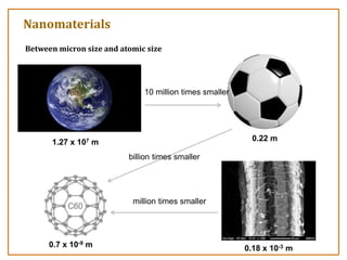
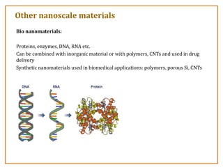
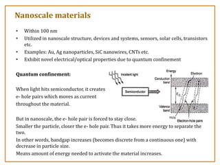
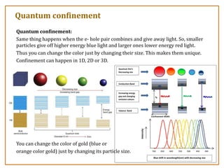
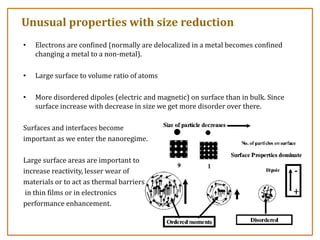
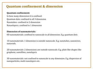
Nanosensors(MEL7420):
Nanomaterials
By: Dr. Shrutidhara Sarma
Department of Mechanical Engineering
IIT Jodhpur
Materials
Natural and Manmade:
Visible rays= 300-600 nm
Human eye resolution =0.07 mm
Grains in a solid
Normal grain size = 1 to 10 microns
Crystalline solids
1 atom= 0.1-0.2 nm
X-rays= 0.1-0.2 nm
Nanomaterials
Between micron size and atomic size
1.27 x 10⁷ m 0.22 m
0.18 x 10⁻³ m
0.7 x 10⁻⁹ m
10 million times smaller
million times smaller
billion times smaller
Other nanoscale materials
Bio nanomaterials:
Proteins, enzymes, DNA, RNA etc.
Can be combined with inorganic material or with polymers, CNTs and used in drug
delivery
Synthetic nanomaterials used in biomedical applications: polymers, porous Si, CNTs
Nanoscale materials
• Within 100 nm
• Utilized in nanoscale structure, devices and systems, sensors, solar cells, transistors
etc.
• Examples: Au, Ag nanoparticles, SiC nanowires, CNTs etc.
• Exhibit novel electrical/optical properties due to quantum confinement
Quantum confinement:
When light hits semiconductor, it creates
e- hole pairs which moves as current
throughout the material.
But in nanoscale, the e- hole pair is forced to stay close.
Smaller the particle, closer the e- hole pair. Thus it takes more energy to separate the
two.
In other words, bandgap increases (becomes discrete from a continuous one) with
decrease in particle size.
Means amount of energy needed to activate the material increases.
Quantum confinement
Quantum confinement:
Same thing happens when the e- hole pair combines and give away light. So, smaller
particles give off higher energy blue light and larger ones lower energy red light.
Thus you can change the color just by changing their size. This makes them unique.
Confinement can happen in 1D, 2D or 3D.
You can change the color of gold (blue or
orange color gold) just by changing its particle size.
Unusual properties with size reduction
• Electrons are confined (normally are delocalized in a metal becomes confined
changing a metal to a non-metal).
• Large surface to volume ratio of atoms
• More disordered dipoles (electric and magnetic) on surface than in bulk. Since
surface increase with decrease in size we get more disorder over there.
Surfaces and interfaces become
important as we enter the nanoregime.
Large surface areas are important to
increase reactivity, lesser wear of
materials or to act as thermal barriers
in thin films or in electronics
performance enhancement.
Quantum confinement & dimension
Quantum confinement:
In how many dimension it is confined:
Quantum dots: confined in all 3 dimension
Nanotubes: confined in 2 dimension
Nanaolayers: confined in 1 dimension
Dimension of nanomaterials:
0D nanomaterials: confined to nanoscale in all dimension. E.g. quantum dots
1D nanomaterials: 1 dimension is outside nanoscale. E.g. nanotubes, nanowires,
nanorods.
2D nanomaterials: 2 dimensions are outside nanoscale. E.g. plate like shapes like
graphene, nanofilms, nanolayers
3D nanomaterials: not confined to nanoscale in any dimension. E.g. dispersion of
nanoparticles, multi-nanolayers etc.

Nanomaterials and quantum confinement.pptx

  • 1.
    Nanosensors(MEL7420): Nanomaterials By: Dr. ShrutidharaSarma Department of Mechanical Engineering IIT Jodhpur
  • 2.
    Materials Natural and Manmade: Visiblerays= 300-600 nm Human eye resolution =0.07 mm
  • 3.
    Grains in asolid Normal grain size = 1 to 10 microns
  • 4.
    Crystalline solids 1 atom=0.1-0.2 nm X-rays= 0.1-0.2 nm
  • 5.
    Nanomaterials Between micron sizeand atomic size 1.27 x 10⁷ m 0.22 m 0.18 x 10⁻³ m 0.7 x 10⁻⁹ m 10 million times smaller million times smaller billion times smaller
  • 6.
    Other nanoscale materials Bionanomaterials: Proteins, enzymes, DNA, RNA etc. Can be combined with inorganic material or with polymers, CNTs and used in drug delivery Synthetic nanomaterials used in biomedical applications: polymers, porous Si, CNTs
  • 7.
    Nanoscale materials • Within100 nm • Utilized in nanoscale structure, devices and systems, sensors, solar cells, transistors etc. • Examples: Au, Ag nanoparticles, SiC nanowires, CNTs etc. • Exhibit novel electrical/optical properties due to quantum confinement Quantum confinement: When light hits semiconductor, it creates e- hole pairs which moves as current throughout the material. But in nanoscale, the e- hole pair is forced to stay close. Smaller the particle, closer the e- hole pair. Thus it takes more energy to separate the two. In other words, bandgap increases (becomes discrete from a continuous one) with decrease in particle size. Means amount of energy needed to activate the material increases.
  • 8.
    Quantum confinement Quantum confinement: Samething happens when the e- hole pair combines and give away light. So, smaller particles give off higher energy blue light and larger ones lower energy red light. Thus you can change the color just by changing their size. This makes them unique. Confinement can happen in 1D, 2D or 3D. You can change the color of gold (blue or orange color gold) just by changing its particle size.
  • 9.
    Unusual properties withsize reduction • Electrons are confined (normally are delocalized in a metal becomes confined changing a metal to a non-metal). • Large surface to volume ratio of atoms • More disordered dipoles (electric and magnetic) on surface than in bulk. Since surface increase with decrease in size we get more disorder over there. Surfaces and interfaces become important as we enter the nanoregime. Large surface areas are important to increase reactivity, lesser wear of materials or to act as thermal barriers in thin films or in electronics performance enhancement.
  • 10.
    Quantum confinement &dimension Quantum confinement: In how many dimension it is confined: Quantum dots: confined in all 3 dimension Nanotubes: confined in 2 dimension Nanaolayers: confined in 1 dimension Dimension of nanomaterials: 0D nanomaterials: confined to nanoscale in all dimension. E.g. quantum dots 1D nanomaterials: 1 dimension is outside nanoscale. E.g. nanotubes, nanowires, nanorods. 2D nanomaterials: 2 dimensions are outside nanoscale. E.g. plate like shapes like graphene, nanofilms, nanolayers 3D nanomaterials: not confined to nanoscale in any dimension. E.g. dispersion of nanoparticles, multi-nanolayers etc.