Introduction nanoscience
•Download as DOCX, PDF•
2 likes•320 views

Engineering Physics study materials discusses nanoscience and nanotechnology. It defines nanotechnology as manipulating matter at the atomic or molecular scale to produce novel structures and devices. When matter is reduced to the nanoscale, quantum confinement occurs and energy levels become quantized. This can increase the band gap and surface area to volume ratio. Nanomaterials are classified based on dimensionality (0D, 1D, 2D) and properties (metallic, semiconducting, insulating). Synthesis methods include top-down (milling) and bottom-up (self-assembly) approaches. Carbon nanotubes are discussed in detail, including their unique electrical, mechanical, and thermal properties, and applications in fields like electronics, composites,

Recommended
Recommended
More Related Content
What's hot
What's hot (20)
Similar to Introduction nanoscience
Similar to Introduction nanoscience (20)
More from Praveen Vaidya
More from Praveen Vaidya (20)
Recently uploaded
Recently uploaded (20)
Introduction nanoscience
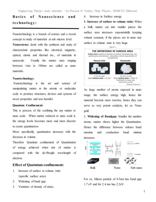
- 1. Engineering Physics study materials – by Praveen N. Vaidya, Dept. Physics, SDMCET Dharwad. 1 B a s ic s o f N a no s c ie nc e a nd te c hno lo g y: Nanotechnology is a branch of science and a recent concept to study of materials at sub micron level. Nanoscience deals with the synthesis and study of characteristic properties like electrical, magnetic, optical, elastic and thermal etc., of materials in nanoscale. Usually the matter sizes ranging between 1nm to 100nm are called as nano materials. Nanotechnology: Nanotechnology is the art and science of manipulating matter at the atomic or molecular scale to produce structures, devices and systems of novel properties and non harmful. Quantum Confinement: This is process of the confining the any matter to nano scale. When matter reduced to nano scale it, the energy levels becomes more and more discrete to create quantization. More specifically, quantization increases with the decrease in volume. Therefore Quantum confinement of Quantization of energy achieved when size of matter is compared with the de-Broglie wavelength of electron. Effect of Quatntum confinement: 1. Increase of surface to volume ratio (specific surface area). 2. Widening of band gap. 3. Variation of density of states. 4. Increase in Surface energy 1. Increase of surface to volume ratio: When a bulk matter cut into smaller pieces the surface area increases exponentially keeping volume constant, if the pieces are in nano size surface to volume ratio is very large. As large number of atoms exposed in nano range, the surface energy high, hence the material become more reactive, hence they can serve as very potent catalysts, for ex. Nano gold 2. Widening of Bandgap: Smaller the number atoms, matter shows higher the Quantization. Hence the difference between valence band maxima and conduction band minima increases. For ex. Silicon particle of 4.5nm has band gap 1.7 eV and for 2.4 nm has 2.2eV. Bulk Nano Sub-nano
- 2. Engineering Physics study materials – by Praveen N. Vaidya, Dept. Physics, SDMCET Dharwad. 2 Classification Nanomaterials: They are classified in two ways 1) Based on the Shape (Direction of confinement) 2) Based on the intrinsic Properties 1. based on shape: (1) zero-dimensional (0-D), (2) One- dimensional (1-D), (3) Two-dimensional (2-D), Zero-dimensional (0-D), Materials in which all the dimensions are confined to nano scale (no dimensions are larger than 100 nm). The zero-dimensional nanomaterials are also called as nanoparticles or Quantum dots. The colour of the nano particles changes with their size. Smaller nano particles show Blue shift where as larger the particle size shows Red shift. The bandgap appears in nano particles and it increases with the decrease in particle size. Hence nanoparticles show quantization of energy levels. One-dimensional nanomaterials The nanomaterials formed by enhancing along one dimension confining other two in nano size are called one dimensional Nano materials. These are also called Quantum wire. Examples, nanotubes (carbon nanotubes), nanorods, and nanowires (Zn nano wire). Two-dimensionalnanomaterials The nanomaterials formed by enhancing along two dimension confining other two in nano size are called two dimensional Nano materials. They are also called nano planes or Quantum planes. For ex. Thin films Density of states: In any material the electrons are moving around the respective atoms in various energy levels. In case of solids each energy level divided into n number of energylevels, if n atoms are present in a 1D L d < 100nm Two dimensions are in Nanoscale
- 3. Engineering Physics study materials – by Praveen N. Vaidya, Dept. Physics, SDMCET Dharwad. 3 piece of material. Hence a group of energy level is called as energy band. In above fig. number atoms along X-axis and Energy along Y-axis. The split of energylevel shown dependent on the number of atoms in solid, if 1023 atoms are there and each atom splits into 2023 energy levels. Similarly, The density of energy states (DOS) i.e. number of energy levels per unit volume also dependent on the energy. DOS increases with energy initially at higher energy, the DOS slowly goes to constant. DOS also dependent on the dimensions confinement. Variation of Density of States in Nano Systems: Let us recall the three dimensional systems like bulk systems, in which the density of states varies as function of square root of energy. As shown in above tables D(E) is the density of states of Nano materials confined in different dimensions. Variation gives smooth curve (Fig. 2.5a). In case bulk materials i.e. no confinement variation of density of states with Energy is given by, D(E) E1/2, In case Two dimensional nano materials i.e. in quantum planes (quantum well), Density of states is independent of Energy. D(E) = Constant, Variation gives step function (fig. 2.5b). In case of One dimensional nano materials i.e. quantum wires, variation of density of states with Energy is given by, D(E) E -1/2, variation gives zig-zag curve(fig. 2.5c). In case of Zero dimensional nano materials or Quantum dots, i.e. electrons are confined in all the dimensions hence no free electrons are available, hence it gives delta function D(E) = 2 (E – Ec) variation is discrete function(fig. 2.5d) Hence it gives aconstant values of density of states at each energy values. Classification based on intrinsic properties: There are three types again 1. Metallic Nanomaterials 2. Semiconducting Nanomaterials 3. Insulator Nanomaterials
- 4. Engineering Physics study materials – by Praveen N. Vaidya, Dept. Physics, SDMCET Dharwad. 4 1. Metallic Nanomaterials: These are nanoderivatives of metals. For Ex. Gold nano particles. Used in catalysis, memory units, sensors, bio sensors etc. 2. Semiconducting Nanomaterials: These are nanosize particles or films of semiconductors. Most semiconducting nanomaterials are made of compound semiconductors. These are used in LED, Laser or any electronic devices. 3. Insulating nanomaterials: These are nanosize materials made of insulators for ex. SiO2 nanomaterials, Diamond nanomaterials. Size dependent Properties: Importance of the nanomaterials is lies behind its changing properties when they are reduced size from bulk to nano and reduction in nano size itself. Physical Properties: When size reduced from bulk nano the surface to volume ratio increases. The appearance of also changes. For ex. Gold powder of nano size appears deep red. Chemical Properties: The reactivity of the materials increases in particle size reduced to nano, due to in complete bonding of surface atoms, these atoms are become highly reactive and acts as catalyst for ex. Bulk gold is inert but nanogold is highly reactive. Thermal Properties Gold slab macro size has melting point 1064 °C, whereas gold nanoparticles melt at much lower temperatures (~300 °C for 2.5 nm size) Optoelectronic Properties Due to increase in bandgap when a material turn into nano, the absorption spectra show blue shift with the reduction of size of nano particles. Magnetic Propeties Ferroelectric materials smaller than 10 nm can switch their magnetization direction using room temperature thermal energy, thus making them unsuitable for memory storage. Mechanical properties: Nanoparticle surface strongly interact with liquid molecules to overcome gravity effect, hence they can be suspended in liquid. The high surface to volume ratio of nanoparticles provides a tremendous driving force for diffusion, especially at elevated temperatures. Clay nanoparticles when incorporated into polymer matrices increase reinforcement, leading to stronger plastics. Synthesis of Nano material: There are two approaches 1) Top down 2) Bottom up Top down Approach: In this method the bulk material is broken into grains of extremely smaller size between 1nm to 100nm. Care should be taken that its crystal structure should not be altered. In this case the powder of cryastal which contains grain micro size is furder grind into controlled conditions to form nano materials.
- 5. Engineering Physics study materials – by Praveen N. Vaidya, Dept. Physics, SDMCET Dharwad. 5 The temperature and grinding is such a way so that crystal structure should not altered Examples Ball millig, In other method, the solid matter is evaporated and sublimate to form a film on a surface called substrate. Here thickness of film is in nano range. Electron lithography, vapor deposition techniques etc. Bottom-up approach refers to the build-up of a material from the bottom: atom-by-atom, molecule-by-molecule, or cluster-by-cluster. In organic chemistry and/or polymer science, we know polymers are synthesized by connecting individual monomers together. In crystal growth, growth species, such as atoms, ions and molecules, after impinging onto the growth surface, assemble into crystal structure one after another. Ex: Solgel, Chemical bath, Spray pyrolysis, Laser ablation etc. Laser ablation Laser ablation means the removal of material from a surface by means of laser irradiation. The term “laser ablation” is used to emphasize the nonequilibrium vapor/plasma conditions created at the surface by intense laser pulse. As shown above diagram, there are two essential parts in the laser ablation device, a pulsed laser (CO2 laser, Nd-YAG laser) and an ablation chamber. The high power of the laser beam induces large light absorption on the surface of target, which makes temperature of the absorbing material increase rapidly. As a result, the material on the surface of target vaporizes into laser plume. In some cases, the vaporized materials condensate into cluster and particle without any chemical reaction. In some other cases, the vaporized material reacts with introduced reactants to form new materials. The condensed particle will be either deposited on a substrate or collected through a filter system consisting of a glass fiber mesh. Then, the collected nanoparticle can be coated on a substrate through drop- coating or screen-printing process. Carbon Nanotubes Carbon Nanotubes first identified in 1991 by Sumio Iijima of Nec, Japan, and formed from hexagonal arrays of carbon atoms. The honeycomb-shaped net in the form of tube, each vertex contain carbon atom which are covalently bond. There two types based on concentric tubes present, 1. Single Walled Carbon Nanotubes (SWCNT): This type of CNTs consists of
- 6. Engineering Physics study materials – by Praveen N. Vaidya, Dept. Physics, SDMCET Dharwad. 6 single cylinder of the one atomic layercarbon sheet. The diameter of cylinder is about 0.7 nm and length may be million times of the diameter. Multi walled nanotubes (MWCNT): The multi walled Carbon Nanotubes consists of more than one concentric rings of carbon nanotubes, whose properties are varies as the function of diameter of the each concentric cylinder. The structure of the nanotube influences its properties - including electrical and thermal conductivity, density, and lattice structure. The Carbon nanotubes are relates to the property of graphite. When graphene sheets are rolled into a cylinder and their edges joined, they form CNTs. Based on shape there are three types of CNTs as shown in figure, a) Arm chair b) Zig Zag c) Chiral Properties of Carbon Nanotubes: a) Electrical Conductivity CNTs can be semiconducting or conducting based on degree of twist as well as their diameter. Conductivity in MWNTs is quite complex. Some types of “armchair”-structured CNTs appear to conduct better than other metallic CNTs. b) Strength and Elasticity Because of strong bonds, the basal plane elastic modulus of graphite is one of the largest of any known material. For this reason, CNTs are expected to be the ultimate high- strength fibers. Thermal Properties: CNTs show very high thermal conductivity. CNTs have been shown to exhibit superconductivity below 20°K (aaprox. - 253°C). The almost zero in-plane thermal expansion but large inter-plane expansion of single walled nanotubes implies strong in- plane coupling and high flexibility against non-axial strains. d) Field Emission:Under the application of a strong electric field, CNTs are showing field emission. Even for moderate voltages, a strong electric field develops at the free end of supported CNTs because of their sharpness. e) Highly Absorbent: The large surface area and high absorbency of CNTs make them ideal candidates for use in air, gas, and water filtration. A lot of research is being done in
- 7. Engineering Physics study materials – by Praveen N. Vaidya, Dept. Physics, SDMCET Dharwad. 7 replacing activated charcoal with CNTs in certain ultra high purity applications. Applications of Carbon Nanotubes: a) Field Emission: Due to best field emitters, CNTs can carry an astonishingly high current density and extremely stable current. This property used in field-emission flat-panel displays, low- voltage cold-cathode lighting sources, lightning arrestors, and electron microscope sources. b) Conductive or Reinforced Plastics: Since CNTs have the highest aspect ratio and have natural tendency to form ropes, Applications that exploit this behavior of CNTs include EMI/RFI shielding composites; transparent conductive coatings; and radar-absorbing materials for stealth applications. c) Conductive Adhesives and Connectors The same properties that make CNTs attractive as conductive fillers for use in electromagnetic shielding, ESD materials, etc., such as adhesives, potting compounds, coaxial cables, and other types of connectors. d) Molecular Electronics The geometry, electrical conductivity, and ability to be precisely derived, make CNTs the ideal candidates for the connections in molecular electronics. In addition, they have been demonstrated as switches themselves. e) Thermal Materials The exceptional Thermal conductivity of CNT found application in electronics, particularly heat sinks for chips used in advanced computing, The technology for creating aligned structures and ribbons of CNTs is a step toward realizing incredibly efficient heat conduits. f) Structural Composites The CNTs show superior mechanical properties, such as stiffness, toughness, and strength. These properties lead to a wealth of applications exploiting them, including advanced composites requiring high values of one or more of these properties. h) Catalyst Support CNTs intrinsically have an enormously high surface area; hence it will get ability to attach essentially any chemical species to their sidewalls through unsatisfied bonds, provides an opportunity for unique catalyst supports.