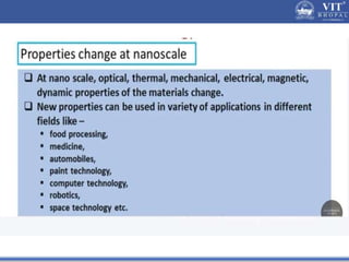
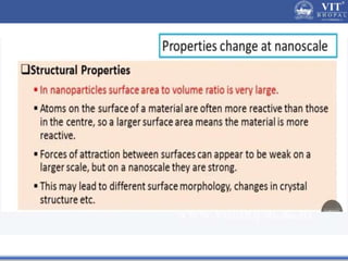
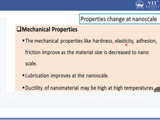
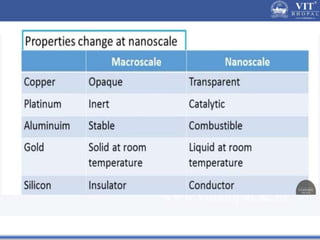
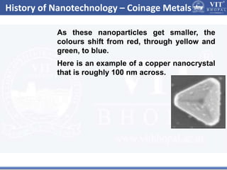
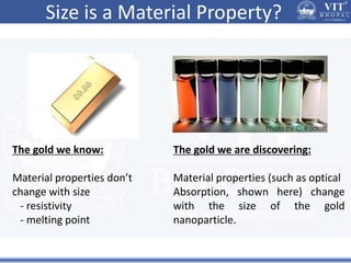
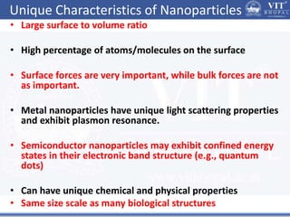
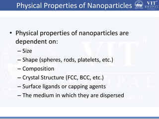
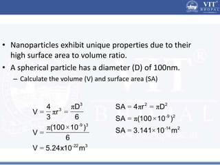
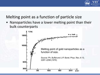
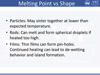
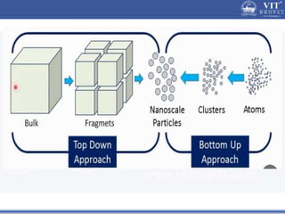
1. Nanoparticles have unique properties due to their high surface area to volume ratio, including lower melting points and tunable optical absorption.
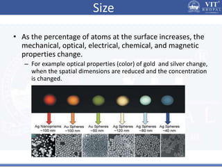
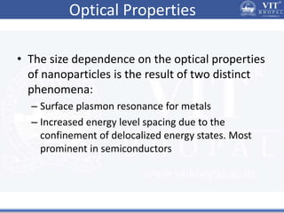
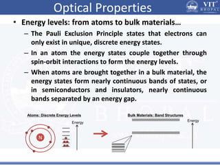
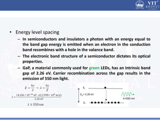
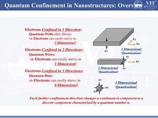
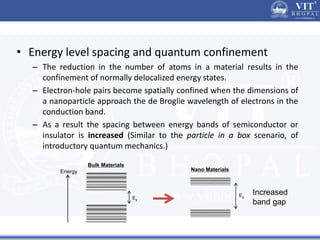
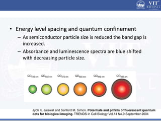
2. In semiconductors, quantum confinement results from physically constraining electrons, increasing the energy level spacing and causing absorption and emission spectra to shift to higher energies with decreasing particle size.
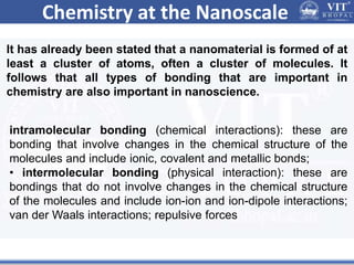
3. Nanomaterials exhibit both intramolecular bonding like covalent and ionic bonds, and intermolecular bonding like van der Waals forces, which influence their physical and chemical properties.