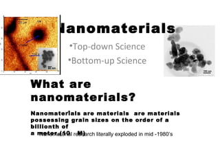
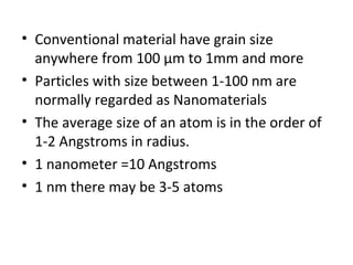
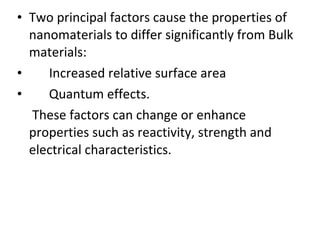
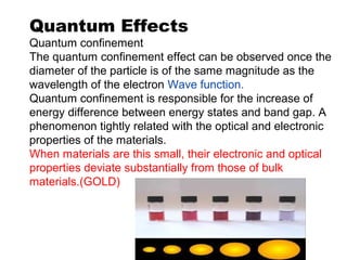
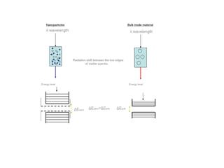
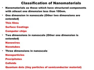
Nanomaterials are materials with at least one dimension sized between 1 to 100 nanometers. They possess unique properties due to their increased surface area to volume ratio and quantum effects. There are several types of nanomaterials including nanoparticles, nanotubes, nanowires, fullerenes and more. Some key aspects are:
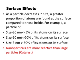
- Nanoparticles have over 50% of their atoms on the surface, increasing reactivity.
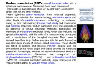
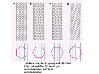
- Carbon nanotubes are very strong and can be semiconducting or metallic depending on their structure.
- Nanomaterials can be synthesized through various methods including chemical vapor deposition and laser ablation.
- Their small size gives nanomaterials potential applications in electronics, optics, medicine and more. However more